 | ÐлекÑÑоннÑй компоненÑ: LT1249 | СкаÑаÑÑ:  PDF PDF  ZIP ZIP |
Äîêóìåíòàöèÿ è îïèñàíèÿ www.docs.chipfind.ru
LT1249
1
Power Factor Controller
s
Standard 8-Pin Packages
s
High Power Factor Over Wide Load Range
with Line Current Averaging
s
International Operation Without Switches
s
Instantaneous Overvoltage Protection
s
Minimal Line Current Dead Zone
s
Typical 250
µ
A Start-Up Supply Current
s
Rejects Line Switching Noise
s
Synchronization Capability
s
Low Quiescent Current: 9mA
s
Fast 1.5A Peak Current Gate Driver
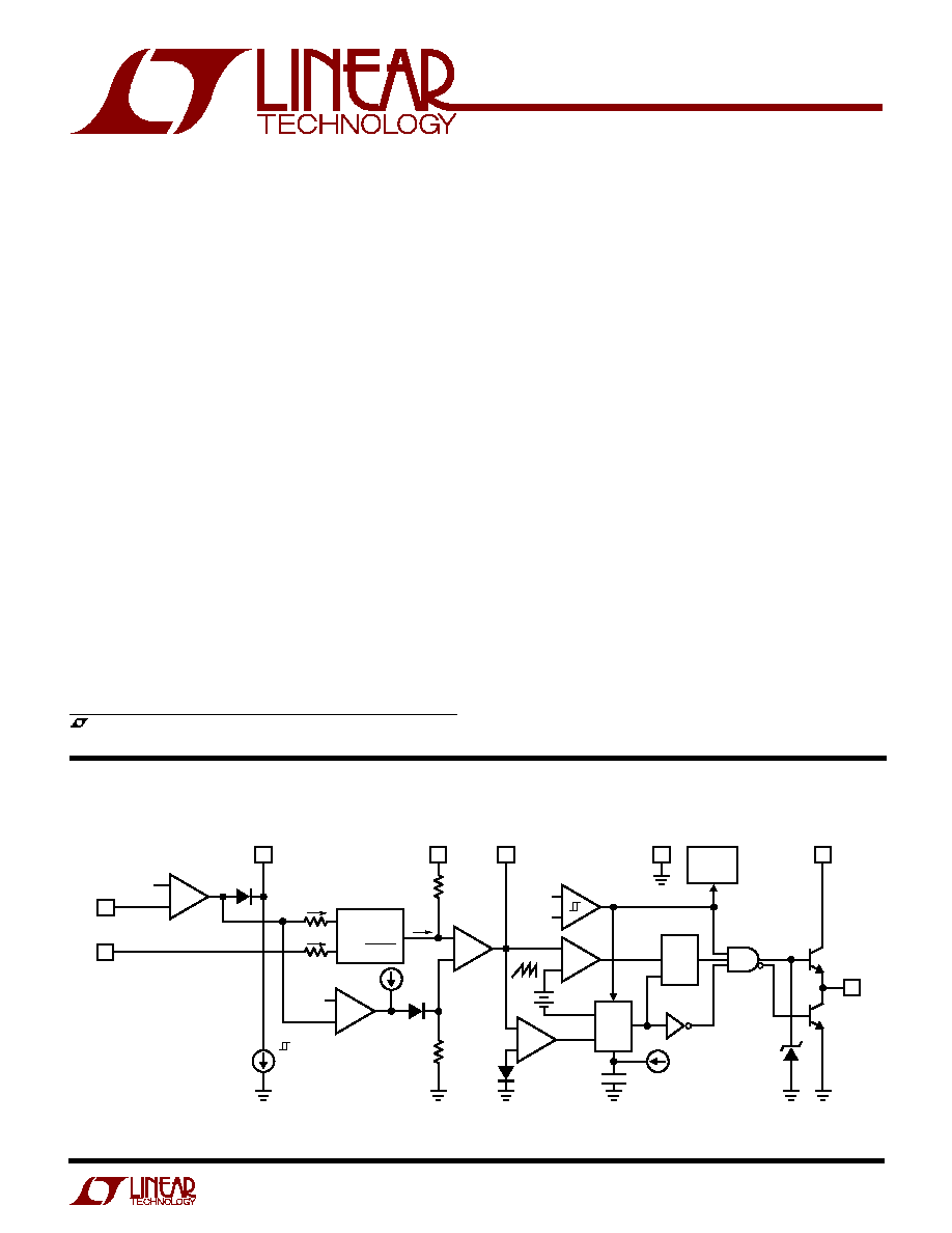
The 8-pin LT
®
1249 provides active power factor correc-
tion for universal offline power systems with very few
external parts. By using fixed high frequency PWM current
averaging without the need for slope compensation, the
LT1249 achieves far lower line current distortion, with a
smaller magnetic element than systems that use either peak
current detection or zero current switching approach, in
both continuous and discontinuous modes of operation.
The LT1249 uses a multiplier containing a square gain
function from the voltage amplifier to reduce the AC gain
at light output load and thus maintains low line current
distortion and high system stability. The LT1249 also
provides filtering capability to reject line switching noise
which can cause instability when fed into the multiplier.
Line current dead zone is minimized with low bias voltage
at the current input to the multiplier.
The LT1249 provides many protection features including
peak current limiting and overvoltage protection. The
switching frequency is internally set at 100kHz.
While the LT1249 simplifies PFC design with minimal
parts count, the LT1248 provides flexibilities in switching
frequency, overvoltage and current limit.
+
+
+
+
+
I
M
=
I
A
2
I
B
200
µ
A
2
VA
OUT
7.5V
44
µ
A
22
µ
A
15
µ
A
1V
EA
+
32k
I
A
I
B
20
µ
A
250
µ
A MAX
I
M
7.5V
V
REF
+
0.7V
OSC
R
S
Q
6
4
5
3
2
1
7
8
35pF
I
AC
V
SENSE
M
OUT
R
MOUT
4k
4k
CA
OUT
V
CC
V
CC
16V/10V
CA
MULTIPLIER
RUN
RUN
16V
GND
GTDR
1249 BD
SYNC
M1
g
m
= 1/3k
, LTC and LT are registered trademarks of Linear Technology Corporation.
s
Universal Power Factor Corrected Power Supplies
s
Preregulators up to 1500W
FEATURES
DESCRIPTIO
U
APPLICATIO S
U
BLOCK DIAGRA
W
2
LT1249
ABSOLUTE
M
AXI
M
U
M
RATINGS
W
W
W
U
PACKAGE/ORDER I
N
FOR
M
ATIO
N
W
U
U
Supply Voltage ....................................................... 27V
GTDR Current Continuous ..................................... 0.5A
GTDR Output Energy (Per Cycle) ............................. 5
µ
J
I
AC
Input Current ................................................. 20mA
V
SENSE
Input Voltage ............................................ V
MAX
M
OUT
Input Current..............................................
±
5mA
Operating Junction Temperature Range
LT1249C ................................................ 0
°
C to 100
°
C
LT1249I ........................................... 40
°
C to 125
°
C
Thermal Resistance (Junction-to-Ambient)
N8 Package ................................................ 100
°
C/W
S8 Package ................................................. 120
°
C/W
Storage Temperature Range ..................65
°
C to 150
°
C
Lead Temperature (Soldering, 10 sec)................. 300
°
C
ELECTRICAL CHARACTERISTICS
The
q
denotes specifications which apply over the operating temperature
range, otherwise specifications are at T
A
= 25
°
C. Maximum operating voltage (V
MAX
) = 25V, V
CC
= 18V, I
AC
= 100
µ
A, CA
OUT
= 3.5V,
VA
OUT
= 5V, no load on any outputs, unless otherwise noted.
PARAMETER
CONDITIONS
MIN
TYP
MAX
UNITS
Overall
Supply Current (V
CC
in Undervoltage Lockout)
V
CC
= Lockout Voltage 0.2V
q
0.25
0.45
mA
Supply Current, On
11.5V
V
CC
V
MAX
, CA
OUT
= 1V
q
8
12
mA
V
CC
Turn-On Threshold
q
15.5
16.5
17.5
V
V
CC
Turn-Off Threshold
q
9.5
10.5
11.5
V
Voltage Amplifier
V
SENSE
Bias Current
V
SENSE
= 0V to 7V
q
25
250
nA
Voltage Amp Gain
70
100
dB
Voltage Amp Unity-Gain Bandwidth
1.5
MHz
Voltage Amp Output High
0
Source Current
50
µ
A
q
10
12
V
Voltage Amp Output Low
0
Sink Current
5
µ
A
q
0.1
0.4
V
Voltage Amp Source Current
q
130
260
450
µ
A
Voltage Amp Sink Current Threshold
Linear Operation, 2V < VA
OUT
< 10V
q
33
44
57
µ
A
Voltage Amp Sink Current Hysteresis
2V < VA
OUT
< 10V
q
14
22.5
30
µ
A
Current Amplifier
Current Amp Offset Voltage
q
±
2
±
15
mV
Current Amp Transconductance
I
CAOUT
=
±
40
µ
A
q
150
320
550
µ
mho
Current Amp Voltage Gain
2.5V
V
CAOUT
7.5V
500
1000
V/V
Current Amp Source Current
V
MOUT
= 1V, I
M
= 0
µ
V
100
145
220
µ
A
Current Amp Sink Current
V
MOUT
= 0.3V, I
M
= 0
µ
A
67
95
125
µ
A
Current Amp Output High
7.4
8.1
V
Current Amp Output Low
1.2
2
V
ORDER PART
NUMBER
T
JMAX
= 125
°
C,
JA
= 100
°
C/W (N8)
T
JMAX
= 125
°
C,
JA
= 120
°
C/W (S8)
Consult factory for Military grade parts.
LT1249CN8
LT1249IN8
LT1249CS8
LT1249IS8
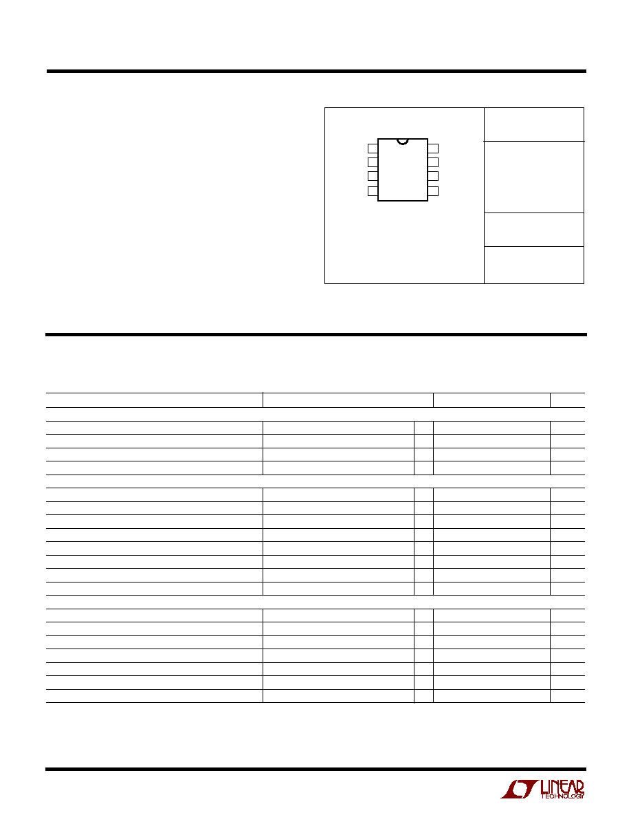
S8 PART
MARKING
1249
1249I
1
2
3
4
8
7
6
5
TOP VIEW
GND
CA
OUT
M
OUT
I
AC
GTDR
V
CC
V
SENSE
VA
OUT
S8 PACKAGE
8-LEAD PLASTIC SO
N8 PACKAGE
8-LEAD PDIP
LT1249
3
Note 1: Absolute Maximum Ratings are those values beyond which the life
of a device may be impaired.
Note 2: Current amplifier is in linear mode with 0V input common mode.
Note 3: Multiplier Gain Constant: K =
Note 4: Maximum GTDR output voltage is internally clamped for higher
V
CC
voltages.
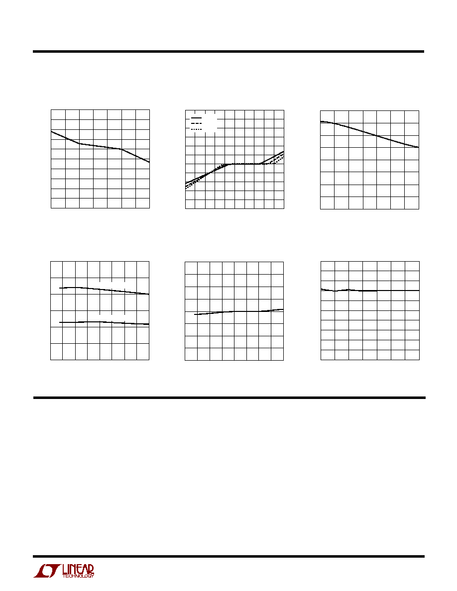
TYPICAL PERFOR
M
A
N
CE CHARACTERISTICS
U
W
FREQUENCY (Hz)
10
GAIN (dB)
100
80
60
40
20
0
20
100
1k
10k
100k
1249 G01
1M
10M
0
20
40
60
80
100
120
PHASE (DEG)
PHASE
GAIN
Voltage Amplifier Open-Loop
Gain and Phase
FREQUENCY (Hz)
1k
TRANSCONDUCTANCE (
µ
mho)
400
350
300
250
200
150
100
50
0
20
0
20
40
60
80
100
120
140
100k
10k
1249 G02
1M
PHASE (DEG)
10M
g
m
Transconductance of
Current Amplifier
I
M
I
AC
(VA
OUT
1.5)
2
PARAMETER
CONDITIONS
MIN
TYP
MAX
UNITS
Reference
Reference Output Voltage
T
A
= 25
°
C, Measured at V
SENSE
Pin
7.39
7.5
7.6
V
Reference Output Voltage Worst Case
All Line, Temperature
q
7.32
7.5
7.68
V
Reference Output Voltage Line Regulation
V
LOCKOUT
< V
CC
< V
MAX
q
20
5
20
mV
Multiplier
Multiplier Output Current
I
AC
= 100
µ
A, VA
OUT
= 5V
35
µ
A
Multiplier Output Current Offset
R
AC
= 1M from I
AC
to GND
q
0.05
0.5
µ
A
Multiplier Max Output Current (I
M(MAX)
)
I
AC
= 450
µ
A, VA
OUT
= 7V (Note 2)
q
375
250
150
µ
A
Multiplier Max Output Voltage (I
M(MAX)
· R
MOUT
)
I
AC
= 450
µ
A, VA
OUT
= 7V (Note 2)
q
1.25
1.1
0.96
V
Multiplier Gain Constant (Note 3)
0.035
V
2
I
AC
Input Resistance
I
AC
from 50
µ
A to 1mA
15
32
50
k
Oscillator
Oscillator Frequency
q
75
100
125
kHz
Control Pin (CA
OUT
) Threshold
Duty Cycle = 0
q
1.3
1.8
2.3
V
Synchronization Frequency Range
Synchronizing Pulse Low
0.35V on CA
OUT
q
127
160
kHz
Gate Driver
Max GTDR Output Voltage
0mA Load, 18V < V
CC
< V
MAX
(Note 4)
q
12
15
17.5
V
GTDR Output High
200mA Load, 11.5V
V
CC
15V
q
V
CC
3.0
V
GTDR Output Low (Device Unpowered)
V
CC
= 0V, 50mA Load (Sinking)
q
0.9
1.5
V
GTDR Output Low (Device Active)
200mA Load (Sinking)
q
0.5
1
V
Peak GTDR Current
10nF from GTDR to GND
2
A
GTDR Rise and Fall Time
1nF from GTDR to GND
25
ns
GTDR Max Duty Cycle
90
96
%
ELECTRICAL CHARACTERISTICS
The
q
denotes specifications which apply over the operating temperature
range, otherwise specifications are at T
A
= 25
°
C. Maximum operating voltage (V
MAX
) = 25V, V
CC
= 18V, I
AC
= 100
µ
A, CA
OUT
= 3.5V,
VA
OUT
= 5V, no load on any outputs, unless otherwise noted.
4
LT1249
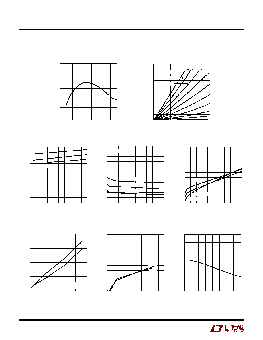
TYPICAL PERFOR
M
A
N
CE CHARACTERISTICS
U
W
I
AC
(
µ
A)
0
I
M
(
µ
A)
300
150
0
1249 G04
250
500
VA
OUT
= 6.5V
VA
OUT
= 6V
VA
OUT
= 5.5V
VA
OUT
= 5V
VA
OUT
= 4.5V
VA
OUT
= 4V
VA
OUT
= 3.5V
VA
OUT
= 3V
VA
OUT
= 2.5V
VA
OUT
= 2V
LOAD CAPACITANCE (nF)
0
TIME (ns)
400
300
200
100
0
10
20
30
40
1249 G08
50
RISE TIME
NOTE: GTDR SLEWS
BETWEEN 1V AND 16V
FALL TIME
Start-Up Supply Current vs
Supply Voltage
Switching Frequency
TEMPERATURE (
°
C)
75
FREQUENCY (kHz)
75
1249 G10
25
25
125
140
130
120
110
100
90
80
70
50
0
50
100
JUNCTION TEMPERATURE (
°
C)
75
REFERENCE VOLTAGE (V)
75
7.536
7.524
7.512
7.500
7.488
7.476
7.464
7.452
7.440
7.428
1249 G03
50
150
25
0
25
50
100 125
SUPPLY VOLTAGE (V)
10
SUPPLY CURRENT (mA)
10
9
8
7
6
5
4
3
2
1
0
26
1249 G05
14
12
16
20
24
28
18
22
30
T
J
= 55
°
C
T
J
= 25
°
C
T
J
= 125
°
C
Supply Current vs Supply Voltage
GTDR Source Current
SOURCE CURRENT (mA)
0
GTDR VOLTAGE (V)
18.5
18.0
17.5
17.0
16.5
16.0
15.5
15.0
14.5
14.0
13.5
13.0
1249 G06
300
T
J
= 25
°
C
T
J
= 125
°
C
V
CC
= 18V
T
J
= 55
°
C
60
120
180
240
GTDR Sink Current
SINK CURRENT (mA)
0
GTDR VOLTAGE (V)
1.1
1.0
0.9
0.8
0.7
0.6
0.5
0.4
0.3
0.2
0.1
0
1249 G07
300
T
A
= 125
°
C
T
A
= 55
°
C
60
120
180
240
T
A
= 25
°
C
GTDR Rise and Fall Time
Reference Voltage vs
Temperature
Multiplier Current
SUPPLY VOLTAGE (V)
0
SUPPLY CURRENT (
µ
A)
550
500
450
400
350
300
250
200
150
100
50
0
1249 G09
20
125
°
C
55
°
C
25
°
C
4
8
12
16
2
6
10
14
18
LT1249
5
PI
N
FU
N
CTIO
N
S
U
U
U
TYPICAL PERFOR
M
A
N
CE CHARACTERISTICS
U
W
TEMPERATURE (
°
C)
SYNCHRONIZATION THRESHOLD (V)
1.0
0.9
0.8
0.7
0.6
0.5
0.4
0.3
0.2
0.1
0
1249 G11
75
25
25
125
50
0
50
100
Synchronization Threshold
at CA
OUT
Voltage Amp Sink Current Limits
(Threshold)
M
OUT
VOLTAGE (V)
2.4
1.2
0
M
OUT
CURRENT (mA)
1.2
1.0
0.8
0.6
0.4
0.2
0
0.2
0.4
0.6
0.8
1.0
1249 G12
1.2
2.4
125
°
C
25
°
C
50
°
C
M
OUT
Pin Characteristics
TEMPERATURE (
°
C)
I
M(MAX)
×
R
MOUT
(V)
1249 G15
1.30
1.25
1.20
1.15
1.10
1.05
1.00
0.95
0.90
75
25
50
25
0
50
100
75
125
Maximum Multiplier Output
Voltage (I
M(MAX)
· R
MOUT
)
Transconductance of Current
Amplifier Over Temperature
TEMPERATURE (
°
C)
50
TRANSCONDUCTANCE (
µ
mho)
100
1249 G13
0
50
400
350
300
250
200
150
100
50
0
25
25
75
125
Maximum Duty Cycle
TEMPERATURE (
°
C)
DUTY CYCLE (%)
100
99
98
97
96
95
94
93
92
91
90
1249 G16
75
25
25
125
50
0
50
100
TEMPERATURE (
°
C)
75
CURRENT (
µ
A)
25
50
25
0
50
100
75
125
1249 G14
60
50
40
30
20
10
0
UP THRESHOLD
DOWN THRESHOLD
NOTE: THESE SINK CURRENT THRESHOLDS ARE
FOR OVERVOLTAGE PROTECTION FUNCTION.
GND (Pin 1): Ground.
CA
OUT
(Pin 2): This is the output of the current amplifier
that senses and forces the line current to follow the
reference signal that comes from the multiplier by com-
manding the pulse width modulator. When CA
OUT
is low,
the modulator has zero duty cycle.
M
OUT
(Pin 3): The multiplier current goes out of this pin
through the 4k resistor R
MOUT
. The voltage developed
across R
MOUT
is the reference voltage of the current loop
and it is limited to 1.1V. The noninverting input of the
current amplifier is also tied to R
MOUT
. In operation, M
OUT
is normally at negative potential and only AC signals
appear at the noninverting input of the current amplifier.
I
AC
(Pin 4): This is the AC line voltage sensing input to the
multiplier. It is a current input that is biased at 2V to
minimize the crossover dead zone caused by low line
voltage. A 32k resistor is in series with the current input,
so that a small external capacitor can be used to filter out
the switching noise from the high impedance lines.
VA
OUT
(Pin 5): This is the output of the voltage error
amplifier. The output is clamped at 12V. When the output
goes below 1.5V, the multiplier output current is zero.