 | –≠–ª–µ–∫—Ç—Ä–æ–Ω–Ω—ã–π –∫–æ–º–ø–æ–Ω–µ–Ω—Ç: LT1020 | –°–∫–∞—á–∞—Ç—å:  PDF PDF  ZIP ZIP |
1
LT1020
Micropower Regulator
and Comparator
S
FEATURE
s
40
µ
A Supply Current
s
125mA Output Current
s
2.5V Reference Voltage
s
Reference Output Sources 1mA and Sinks 0.5mA
s
Dual Output Comparator
s
Comparator Sinks 10mA
s
Dropout Detector
s
0.2V Dropout Voltage
s
Thermal Limiting
s
Available in SO Package
U
S
A
O
PPLICATI
s
Battery Systems
s
Battery Backup Systems
s
Portable Terminals
s
Portable Instruments
The LT1020 is a combination micropower positive regula-
tor and free collector comparator on a single monolithic
chip. With only 40
µ
A supply current, the LT1020 can
supply over 125mA of output current. Input voltage range
is from 4.5V to 36V and dropout voltage is 0.6V at 125mA.
Dropout voltage decreases with lower load currents. Also
included on the chip is a class B output 2.5V reference that
can either source or sink current. A dropout detector
provides an output current to indicate when the regulator
is about to drop out of regulation.
The dual output comparator can be used as a comparator
for system or battery monitoring. For example, the com-
parator can be used to warn of low system voltage while
the dropout detector shuts down the system to prevent
abnormal operation. Frequency compensation of the com-
parator for amplifier applications can be obtained by
adding external output capacitance. Dual output or posi-
tive and negative regulators can also be made.
The 2.5V reference will source or sink current. This allows
it to be used as a supply splitter or auxiliary output.
D
U
ESCRIPTIO
U
A
O
PPLICATI
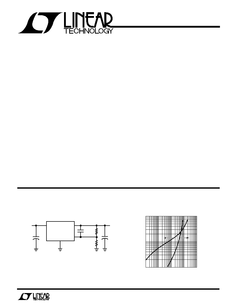
TYPICAL
5V Regulator
Dropout Voltage and Supply Current
+
V
IN
> 5.2V
I
Q
= 40
µ
A
10
µ
F
10
µ
F
0.001
µ
F
1M
1M
5V
2
11
3
9
V
IN
V
OUT
FB
GND
+
LT1020
1020 TA01
OUTPUT CURRENT (mA)
0.1
0.01
DROPOUT VOLTAGE (V)
0.1
1
10
1000
1020 TA02
1
100
0.1
1
10
SUPPLY CURRENT (mA)

2
LT1020
A
U
G
W
A
W
U
W
A
R
BSOLUTE
XI
TI
S
Input Voltage .......................................................... 36V
NPN Collector Voltage ............................................ 36V
PNP Collector Voltage.............................. Supply ≠ 36V
Output Short Circuit Duration ......................... Indefinite
Power Dissipation .............................. Internally Limited
Storage Temperature Range ................ ≠ 65
∞
C to 150
∞
C
Operating Temperature Range
LT1020C ............................................. 0
∞
C to 100
∞
C
LT1020I ........................................ ≠ 40
∞
C to 100
∞
C
LT1020M ....................................... ≠ 55
∞
C to 125
∞
C
Lead Temperature (Soldering, 10 sec) .................. 300
∞
C
W
U
U
PACKAGE/ORDER I FOR ATIO
T
JMAX
= 150
∞
C,
JA
= 80
∞
C/W (J)
T
JMAX
= 110
∞
C,
JA
= 130
∞
C/W (N)
T
JMAX
= 110
∞
C,
JA
= 150
∞
C/W
ORDER PART
NUMBER
T
J
= 25
∞
C
ELECTRICAL C
C
HARA TERISTICS
PARAMETER
CONDITIONS
MIN
TYP
MAX
UNITS
Reference
Reference Voltage
4.5V
V
IN
36V
2.46
2.50
2.54
V
Line Regulation
4.5V
V
IN
36V
0.01
0.015
%/V
Load Regulation
≠ 0.5mA
I
REF
1mA, V
IN
= 12V
0.2
0.3
%
Output Source Current
V
IN
= 5V
1
4
mA
Output Sink Current
V
IN
= 5V
0.5
2
mA
Temperature Stability
1
%
Regulator
Supply Current
V
IN
= 6V, I
OUT
100
µ
A
45
80
µ
A
V
IN
= 36V, I
OUT
100
µ
A
75
120
µ
A
V
IN
= 12V, I
OUT
= 125mA
11
20
mA
Output Current
(V
IN
≠ V
OUT
)
1V, V
IN
6V
125
mA
Load Regulation
(V
IN
≠ V
OUT
)
1V, V
IN
6V
0.2
0.5
%
Line Regulation
6V
V
IN
36V
0.01
0.015
%/V
Dropout Voltage
I
OUT
= 100
µ
A
0.02
0.05
V
I
OUT
= 125mA
0.4
0.65
V
Feedback Sense Voltage
V
IN
= 12V
2.44
2.5
2.56
V
Dropout Detector Current
V
OUT
= ≠ 0.05V, I
OUT
= 500
µ
A
3
20
µ
A
LT1020CJ
LT1020CN
LT1020IJ
LT1020IN
LT1020MJ
ORDER PART
NUMBER
LT1020CS
LT1020IS
1
2
3
4
5
6
7
TOP VIEW
J PACKAGE
14-LEAD CERAMIC DIP
N PACKAGE
14-LEAD PLASTIC DIP
14
13
12
11
10
9
8
NC
V
OUT
V
IN
REF OUT
COMP PNP
COMP NPN
+INPUT
NC
SHUTDOWN
FEEDBACK
GND
≠INPUT
DROPOUT
DETECTOR
CURRENT
LIMIT
TOP VIEW
S PACKAGE
16-LEAD PLASTIC SOIC
1
2
3
4
5
6
7
8
16
15
14
13
12
11
10
9
NC
V
OUT
VI
N
REF OUT
COMP PNP
COMP NPN
+INPUT
NC
NC
SHUTDOWN
FEEDBACK
GND
≠INPUT
NC
DROPOUT
DETECTOR
CURRENT
LIMIT

3
LT1020
T
J
= 25
∞
C
ELECTRICAL C
C
HARA TERISTICS
ELECTRICAL C
C
HARA TERISTICS
PARAMETER
CONDITIONS
MIN
TYP
MAX
UNITS
Regulator
Feedback Bias Current
15
40
nA
Minimum Load Current
V
IN
= 36V
1
5
µ
A
Short-Circuit Current
V
IN
= 36V
300
400
mA
Pins 9 and 10 Shorted, V
IN
= 4.5V
3
30
mA
Comparator
Offset Voltage
0V
V
CM
35V, V
IN
= 36V
3
7
mV
Bias Current
0V
V
CM
35V, V
IN
= 36V
15
40
nA
Offset Current
0V
V
CM
35V, V
IN
= 36V
4
15
nA
Gain-NPN Pull-Down
V
OUT
= 29V, R
L
= 20k
2000
10000
V/ V
Common-Mode Rejection
0V
V
CM
35V, V
IN
= 36V
80
94
dB
Power Supply Rejection
4.5V
V
S
36V
80
96
dB
Output Sink Current
V
IN
= 4.5V
10
18
mA
NPN Saturation Voltage
I
OUT
= 1mA
0.4
0.6
V
Output Source Current
60
200
µ
A
Input Voltage Range
0
V
IN
≠ 1
V
Response Time
5
µ
s
Leakage Current (NPN)
2
µ
A
PARAMETER
CONDITIONS
MIN
TYP
MAX
UNITS
Reference
Reference Voltage
4.5V
V
IN
36V
q
2.40
2.50
2.55
V
Line Regulation
4.5V
V
IN
36V
q
0.01
0.02
%/V
Load Regulation
≠ 0.5mA
I
REF
1mA, V
IN
= 12V
q
0.3
0.4
%
Output Source Current
V
IN
= 5V
q
1
mA
Output Sink Current
V
IN
= 5V
q
0.5
mA
Regulator
Supply Current
V
IN
= 6V, I
OUT
100
µ
A
q
65
95
µ
A
V
IN
= 36V, I
OUT
100
µ
A
q
85
120
µ
A
V
IN
= 12V, I
OUT
= 125mA
q
11
20
mA
Output Current
(V
IN
≠ V
OUT
)
1V, V
IN
6V
q
125
mA
Load Regulation
(V
IN
≠ V
OUT
)
1V, V
IN
6V
q
1
%
Line Regulation
6V
V
IN
36V
q
0.02
%/ V
Dropout Voltage
I
OUT
= 100
µ
A
q
0.06
V
I
OUT
= 125mA
q
0.85
V
Feedback Sense Voltage
V
IN
= 12V
q
2.38
2.5
2.57
V
Dropout Detector Current
V
OUT
= ≠ 0.05V, I
OUT
= 500
µ
A
q
3
µ
A
Feedback Bias Current
q
50
nA
Minimum Load Current
V
IN
= 36V
q
50
µ
A
Short-Circuit Current
V
IN
= 36V
q
300
400
mA
Pins 9 and 10 Shorted, V
IN
= 4.5V
q
2.5
30
mA
Comparator
Offset Voltage
0V
V
CM
35V, V
IN
= 36V
q
10
mV
Bias Current
0V
V
CM
35V, V
IN
= 36V (Note 1)
q
15
60
nA
Offset Current
0V
V
CM
35V, V
IN
= 36V
q
20
nA
Gain-NPN Pull-Down
V
OUT
= 29V, R
L
= 20k
q
1000
V/ V

4
LT1020
ELECTRICAL C
C
HARA TERISTICS
C
C
HARA TERISTICS
U
W
A
TYPICAL PERFOR
CE
OUTPUT CURRENT (mA)
OUTPUT VOLTAGE CHANGE (%)
0.3
0.2
0.1
0
≠0.1
≠0.2
≠0.3
0.1
10
100
1000
1020 G01
1
T
J
= ≠55∞C
T
J
= 25∞C
T
J
= 125∞C
PRELOAD = 100
µ
A
Regulator Short-Circuit Current
TEMPERATURE (∞C)
≠50
SHORT-CIRCUIT CURRENT (mA)
350
300
250
200
150
100
50
0
1020 G03
30
150
≠10
70
110
CURRENT LIMIT TIED TO GROUND
Regulator Load Regulation
Dropout Voltage
Dropout Voltage
REGULATOR OUTPUT CURRENT (mA)
0.1
0.01
INPUT/OUTPUT DIFFERENTIAL (V)
0.1
1
1
10
100
1020 G06
I DROPOUT DETECTOR = 0.1% I
OUT
I DROPOUT DETECTOR = 1% I
OUT
Dropout Voltage
Note 1: For 0V
V
CM
0.1V and T > 85
∞
C I
BIAS(MAX)
is 100nA.
Note 2: For T
A
≠ 40
∞
C output I
SINK(MIN)
is 2.5mA.
PARAMETER
CONDITIONS
MIN
TYP
MAX
UNITS
Comparator
Common-Mode Rejection
0V
V
CM
35V, V
IN
= 36V
q
80
dB
Power Supply Rejection
4.5V
V
IN
36V
q
80
dB
Output Sink Current
V
IN
= 4.5V (Note 2)
q
5
10
mA
Output Source Current
q
40
120
µ
A
Input Voltage Range
q
0
V
IN
≠ 1
V
Leakage Current (NPN)
V
IN
= 36V
q
8
µ
A
The
q
denotes specifications which apply over the full operating
temperature range.
REGULATOR OUTPUT CURRENT (mA)
SUPPLY CURRENT (mA)
100
10
1
0.1
0.01
0.1
10
100
1000
1020 G02
1
T
J
= ≠55∞C TO 125∞C
Supply Current
REGULATOR OUTPUT CURRENT (mA)
0.1
0.01
REGULATOR INPUT/OUTPUT DIFFERENTIAL (V)
0.1
1
10
1000
1020 G04
1
100
V
OUT
= 100mV
REGULATOR OUTPUT CURRENT (mA)
0.1
0.01
REGULATOR INPUT/OUTPUT DIFFERENTIAL (V)
0.1
1
10
1000
1020 G05
1
100
DROPOUT DETECTOR = 5
µ
A

5
LT1020
C
C
HARA TERISTICS
U
W
A
TYPICAL PERFOR
CE
RIPPLE FREQUENCY (Hz)
10
RIPPLE REJECTION (dB)
70
65
60
55
50
45
40
35
30
100
1k
1020 G10
10k
100k
I
OUT
= 100mA
I
OUT
= 10mA
I
OUT
= 1mA
V
IN
= 100VDC, 1V
P-P
V
OUT
= 5V
C
OUT
= 10
µ
F
Regulator Ripple Rejection
REGULATOR INPUT/OUTPUT DIFFERENTIAL (V)
1
SUPPLY CURRENT (mA)
10
1
0.1
0.01
5
1020 G11
I
OUT
= 100mA
10
15
20
25
I
OUT
= 1mA
I
OUT
= 10mA
V
OUT
= 5V
T
J
= ≠55∞C TO 125∞C
Supply Current
REGULATOR OUTPUT CURRENT (mA)
0.1
FEEDBACK PIN CURRENT (nA)
40
35
30
25
20
15
10
5
0
1
10
1020 G15
100
1000
T
J
= 125∞C
T
J
= 25∞C
T
J
= ≠55∞C
Supply Current at Dropout
Feedback Pin Current
Comparator Input Bias Current
COMMON-MODE VOLTAGE (V)
REFERRED TO PIN 9 (GND)
≠1.0
INPUT BIAS CURRENT (nA)
100
90
80
70
60
50
40
30
20
10
0
0.6
1020 G14
≠0.6
≠0.2
0.2
1.0
T
J
= 125∞C
GND
T
J
= 25∞C
T
J
= ≠55∞C
Reference Regulation
REGULATOR INPUT/OUTPUT DIFFERENTIAL (V)
0
DROPOUT DETECTOR CURRENT (
µ
A)
1000
100
10
1
0.1
1020 G08
I
OUT
= 100mA
0.2
0.3
0.4
0.6
0.5
I
OUT
= 25mA
I
OUT
= 1mA
I
OUT
= 5mA
REGULATOR OUTPUT CURRENT (mA)
0.1
DROPOUT DETECTOR CURRENT (
µ
A)
1
10
100
10
1000
1020 G07
0.01
100
V
DIFF
= 500mV
V
DIFF
= 1V
Dropout Detector Current
Dropout Detector Current
TEMPERATURE (∞C)
90
1
10
100
110
130
1020 G09
MINIMUM LOAD CURRENT (
µ
A)
70
150
80
100
120
140
Regulator Minimum Load Current
REGULATOR INPUT/OUTPUT DIFFERENTIAL (V)
0
SUPPLY CURRENT (mA)
10
1
0.1
0.01
0.1
1020 G12
I
OUT
= 100mA
0.2
0.3
0.4
0.6
0.5
I
OUT
= 10mA
I
OUT
= 1mA
T
J
= ≠55∞C TO 125∞C
REFERENCE OUTPUT CURRENT (mA)
≠1.5
REFERENCE VOLTAGE CHANGE (mV)
≠1.0
0
1.0
1.5
1020 G13
4
3
2
1
0
≠1
≠2
≠3
≠4
≠0.5
0.5