 | ÐлекÑÑоннÑй компоненÑ: IRS2110 | СкаÑаÑÑ:  PDF PDF  ZIP ZIP |
Äîêóìåíòàöèÿ è îïèñàíèÿ www.docs.chipfind.ru
HIN
up to 500 V or 600 V
TO
LOAD
V
DD
V
B
V
S
HO
LO
COM
HIN
LIN
V
SS
SD
V
CC
LIN
V
DD
SD
V
SS
V
CC
Features
·
Floating channel designed for bootstrap operation
·
Fully operational to +500 V or +600 V
·
Tolerant to negative transient voltage, dV/dt immune
·
Gate drive supply range from 10 V to 20 V
·
Undervoltage lockout for both channels
·
3.3 V logic compatible
·
Separate logic supply range from 3.3 V to 20 V
·
Logic and power ground ±5V offset
·
CMOS Schmitt-triggered inputs with pull-down
·
Cycle by cycle edge-triggered shutdown logic
·
Matched propagation delay for both channels
·
Outputs in phase with inputs
Description
HIGH AND LOW SIDE DRIVER
Product Summary
VOFFSET (IRS2110)
500 V max.
(IRS2113)
600 V max.
I
O+/-
2 A/2 A
VOUT
10 V - 20 V
ton/off (typ.)
130 ns & 120 ns
Delay Matching (IRS2110) 10 ns max.
(IRS2113) 20 ns max.
www.irf.com
1
The IRS2110/IRS2113 are high voltage, high speed
power MOSFET and IGBT drivers with independent
high and low side referenced output channels. Pro-
prietary HVIC and latch immune CMOS technologies
enable ruggedized monolithic construction. Logic in-
puts are compatible with standard CMOS or LSTTL
output, down to 3.3 V logic. The output drivers feature
a high pulse current buffer stage designed for mini-
mum driver cross-conduction. Propagation delays are
matched to simplify use in high frequency applications.
The floating channel can be used to drive an N-chan-
nel power MOSFET or IGBT in the high side configura-
tion which operates up to 500 V or 600 V.
IRS2110(-1,-2,S)PbF
IRS2113(-1,-2,S)PbF
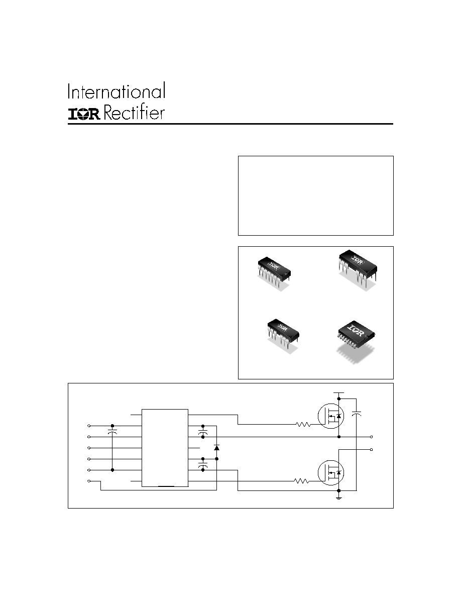
(Refer to Lead Assignments for correct pin configuration). This diagram shows electrical connec-
tions only. Please refer to our Application Notes and DesignTips for proper circuit board layout.
Typical Connection
PRELIMINARY
Packages
14-Lead PDIP
IRS2110 and IRS2113
14-Lead PDIP
(w/o lead 4)
IRS2110-1 and IRS2113-1
16-Lead PDIP
(w/o leads 4 & 5)
IRS2110-2 and IRS2113-2
16-Lead SOIC
IRS2110S and
IRS2113S
Data Sheet No. PD60249 revB
PRELIMINARY
www.irf.com
2
IRS2110(-1,-2,S)PbF/IRS2113(-1,-2,S)PbF
Recommended Operating Conditions
The input/output logic timing diagram is shown in Fig. 1. For proper operation, the device should be used within the
recommended conditions. The VS and VSS offset ratings are tested with all supplies biased at a 15 V differential.
Typical ratings at other bias conditions are shown in Figs. 36 and 37.
Note 2: Logic operational for V
S
of -4 V to +500 V. Logic state held for V
S
of -4 V to -V
BS
. (Refer to the Design Tip DT97-3)
Note 3: When V
DD
< 5 V, the minimum V
SS
offset is limited to -V
DD.
Absolute Maximum Ratings
Absolute maximum ratings indicate sustained limits beyond which damage to the device may occur. All voltage param-
eters are absolute voltages referenced to COM. The thermal resistance and power dissipation ratings are measured
under board mounted and still air conditions. Additional information is shown in Figs. 28 through 35.
Symbol
Definition
Min.
Max.
Units
V
B
High side floating supply voltage
(IRS2110)
-0.3
520 (Note 1)
(IRS2113)
-0.3
620 (Note 1)
V
S
High side floating supply offset voltage
V
B
- 20
V
B
+ 0.3
V
HO
High side floating output voltage
V
S
- 0.3
V
B
+ 0.3
V
CC
Low side fixed supply voltage
-0.
3 2
0
(Note 1)
V
LO
Low side output voltage
-0.3
V
CC
+ 0.3
V
DD
Logic supply voltage
-0
.3
V
SS
+
20
(Note 1)
V
SS
Logic supply offset voltage
V
CC
- 20
V
CC
+ 0.3
V
IN
Logic input voltage (HIN, LIN, & SD)
V
SS
- 0.3
V
DD
+ 0.3
dV
s
/dt
Allowable offset supply voltage transient (Fig. 2)
--
50
V/ns
P
D
Package power dissipation @ T
A
+25
°
C
(14 lead DIP)
--
1.6
(16 lead SOIC)
--
1.25
R
THJA
Thermal resistance, junction to ambient
(14 lead DIP)
--
75
(16 lead SOIC)
--
100
T
J
Junction temperature
--
150
T
S
Storage temperature
-55
150
T
L
Lead temperature (soldering, 10 seconds)
--
300
°
C/W
W
V
°
C
Symbol
Definition
Min.
Max.
Units
V
B
High side floating supply absolute voltage
V
S
+ 10
V
S
+ 20
V
S
High side floating supply offset voltage
(IRS2110)
Note 2
500
(IRS2113)
Note 2
600
V
HO
High side floating output voltage
V
S
V
B
V
CC
Low side fixed supply voltage
10
20
V
LO
Low side output voltage
0
V
CC
V
DD
Logic supply voltage
V
SS
+ 3
V
SS
+ 20
V
SS
Logic supply offset voltage
-5 (Note 3)
5
V
IN
Logic input voltage (HIN, LIN & SD)
V
SS
V
DD
T
A
Ambient temperature
-40
125
°
C
V
Note 1: All supplies are fully tested at 25 V, and an internal 20 V clamp exists for each supply.
www.irf.com
3
IRS2110(-1,-2,S)PbF/IRS2113(-1,-2,S)PbF
PRELIMINARY
Symbol
Definition
Figure Min.
Typ. Max. Units Test Conditions
t
on
Turn-on propagation delay
7
--
130
160
V
S
= 0 V
t
off
Turn-off propagation delay
8
--
120
150
t
sd
Shutdown propagation delay
9
--
130
160
t
r
Turn-on rise time
10
--
25
35
t
f
Turn-off fall time
11
--
17
25
MT
Delay matching, HS & LS (IRS2110)
--
--
--
10
turn-on/off
(IRS2113)
--
--
--
20
ns
Dynamic Electrical Characteristics
V
BIAS
(V
CC
, V
BS
, V
DD
) = 15 V, C
L
= 1000 pF, T
A
= 25
°
C and V
SS
= COM unless otherwise specified. The dynamic
electrical characteristics are measured using the test circuit shown in Fig. 3.
Symbol
Definition
Figure Min.
Typ. Max. Units Test Conditions
V
IH
Logic "1" input voltage
12
9.5
--
--
V
IL
Logic "0" input voltage
13
--
--
6.0
V
OH
High level output voltage, V
BIAS
- V
O
14
--
--
1.2
I
O
= 0 A
V
OL
Low level output voltage, V
O
15
--
--
0.15
I
O
= 20 mA
I
LK
Offset supply leakage current
16
--
--
50
V
B
=V
S
= 500 V/600 V
I
QBS
Quiescent V
BS
supply current
17
--
125
230
I
QCC
Quiescent V
CC
supply current
18
--
180
340
I
QDD
Quiescent V
DD
supply current
19
--
15
30
I
IN+
Logic "1" input bias current
20
--
20
40
V
IN
= V
DD
I
IN-
Logic "0" input bias current
21
--
--
1.0
V
IN
= 0 V
V
BSUV+
V
BS
supply undervoltage positive going
22
7.5
8.6
9.7
threshold
V
BSUV-
V
BS
supply undervoltage negative going
23
7.0
8.2
9.4
threshold
V
CCUV+
V
CC
supply undervoltage positive going
24
7.4
8.5
9.6
threshold
V
CCUV-
V
CC
supply undervoltage negative going
25
7.0
8.2
9.4
threshold
I
O+
Output high short circuit pulsed current
26
2.0
2.5
--
V
O
= 0 V, V
IN
= V
DD
PW
10
µ
s
I
O-
Output low short circuit pulsed current
27
2.0
2.5
--
V
O
= 15 V, V
IN
= 0V
PW
10
µ
s
Static Electrical Characteristics
V
BIAS
(V
CC
, V
BS
, V
DD
) = 15 V, T
A
= 25
°
C and V
SS
= COM
unless otherwise specified. The V
IN
, V
TH,
and I
IN
parameters
are referenced to V
SS
and are applicable to all three logic input leads: HIN, LIN, and SD. The V
O
and I
O
parameters are
referenced to COM and are applicable to the respective output leads: HO or LO.
V
µ
A
V
A
V
S
= 500 V/600 V
V
IN
= 0 V or V
DD
PRELIMINARY
www.irf.com
4
IRS2110(-1,-2,S)PbF/IRS2113(-1,-2,S)PbF
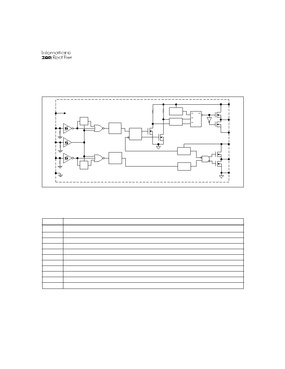
Functional Block Diagram
Lead Definitions
Symbol
Description
V
B
SD
LIN
V
DD
PULSE
GEN
R
S
Q
V
SS
UV
DETECT
DELAY
HV
LEVEL
SHIFT
V
CC
PULSE
FILTER
UV
DETECT
V
DD
/V
CC
LEVEL
SHIFT
V
DD
/V
CC
LEVEL
SHIFT
LO
V
S
COM
R
S
Q
R
S
R
Q
HIN
HO
V
DD
Logic supply
HIN
Logic input for high side gate driver output (HO), in phase
SD
Logic input for shutdown
LIN
Logic input for low side gate driver output (LO), in phase
V
SS
Logic ground
V
B
High side floating supply
HO
High side gate drive output
V
S
High side floating supply return
V
CC
Low side supply
LO
Low side gate drive output
COM
Low side return
www.irf.com
5
IRS2110(-1,-2,S)PbF/IRS2113(-1,-2,S)PbF
PRELIMINARY
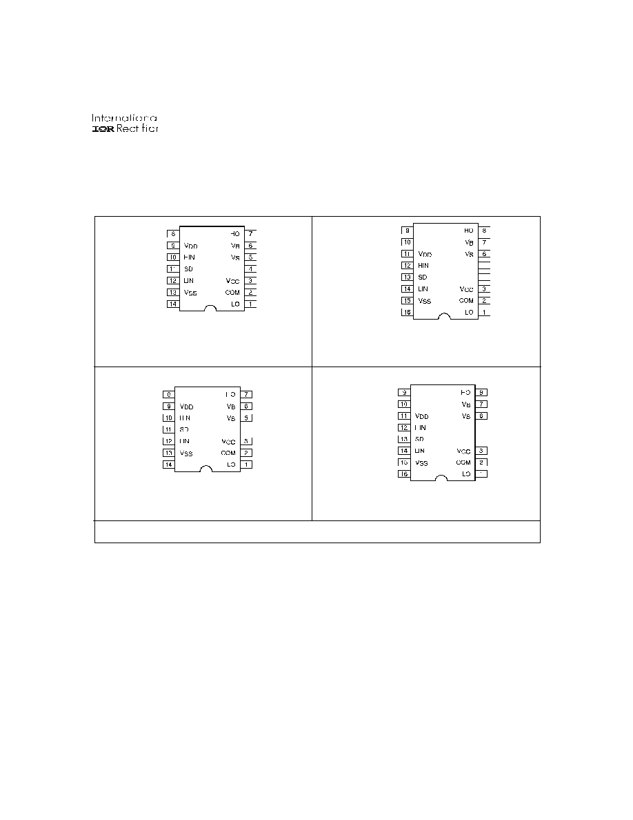
Lead Assignments
Part Number
14 Lead PDIP
IRS2110/IRS2113
16 Lead SOIC (Wide Body)
IRS2110S/IRS2113S
14 Lead PDIP w/o lead 4
IRS2110-1/IRS2113-1
16 Lead PDIP w/o leads 4 & 5
IRS2110-2/IRS2113-2