 | ÐлекÑÑоннÑй компоненÑ: IR51HD214 | СкаÑаÑÑ:  PDF PDF  ZIP ZIP |
Äîêóìåíòàöèÿ è îïèñàíèÿ www.docs.chipfind.ru
Data Sheet No. PD-6.058D
IR51HD214
SELF-OSCILLATING HALF-BRIDGE
Features
n
Output Power MOSFETs in half-bridge configuration
250V Rated Breakdown Voltage
n
High side gate drive designed for bootstrap operation
n
Bootstrap diode integrated into package
n
Accurate timing control for both Power MOSFETs
Matched delay to get 50% duty cycle
Matched deadtime of 1.2us
n
Internal oscillator with programmable frequency
f
=
+
1
1 4
R
75
C
T
T
. × (
) ×
n
Zener clamped Vcc for offline operation
n
Half-bridge output is out of phase with R
T
Description
The IR51HD214 is a high voltage, high speed, self-
oscillating half-bridge. Proprietary HVIC and latch
immune CMOS technologies, along with the
HEXFET® power MOSFET technology, enable
ruggedized single package construction. The front-end
features a programmable oscillator which functions
similar to the CMOS 555 timer. The supply to the
control circuit has a zener clamp to simplify offline
operation. The output features two HEXFETs in a
half-bridge configuration with an internally set
deadtime designed for minimum cross-conduction in
the half-bridge. Propagation delays for the high and
low side power MOSFETs are matched to simplify use
in 50% duty cycle applications. The device can
operate up to 250 volts.
Product Summary
V
IN
(max)
250V
Duty Cycle
50%
Deadtime
1.2µs
R
DS(on)
2.0
P
D
(T
A
= 25 ºC)
2.0W
Package
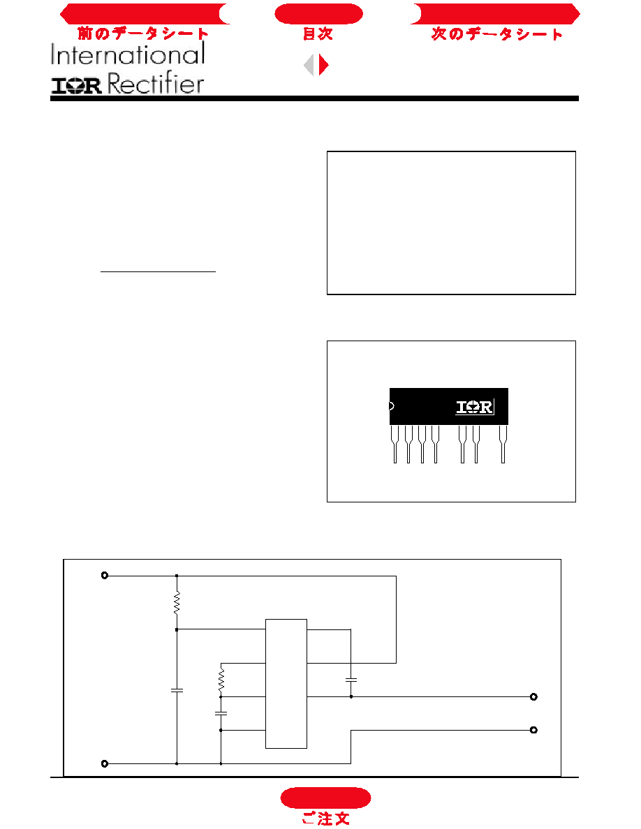
IR51HD214
9506
Typical Connection
T O L O A D
I R 5 1 H D 2 1 4
C O M
C C
V
V I N
B
V
C T
R T
U P T O 2 5 0 V D C B U S
V O
C O M
V I N
T
R
T
C
1
2
3
4
6
9
7
Next Data Sheet
Index
Previous Datasheet
To Order
IR51HD214
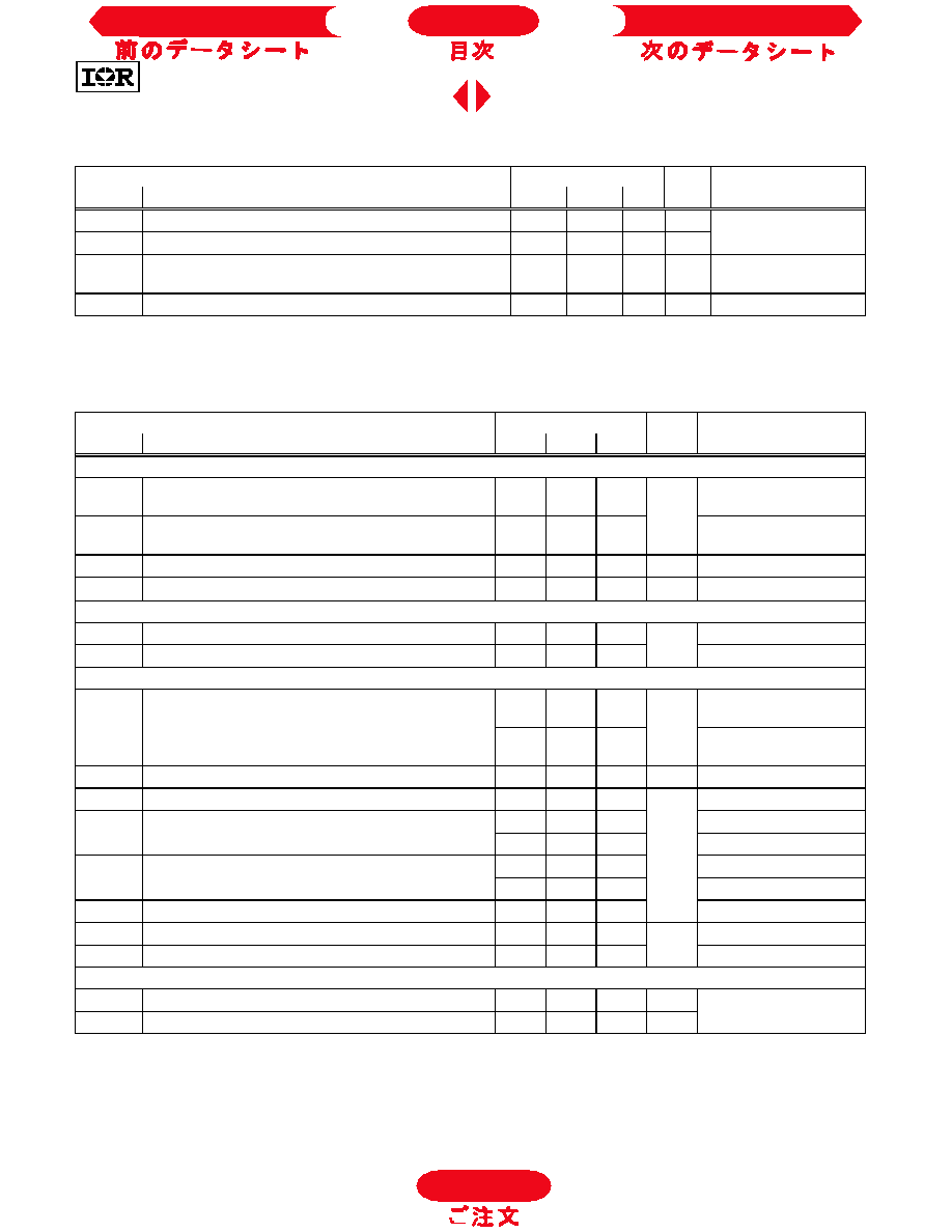
Absolute Maximum Ratings
Absolute Maximum Ratings indicate sustained limits beyond which damage to the device may occur. All
voltage parameters are absolute voltages referenced to COM, all currents are defined positive into any lead.
The Thermal Resistance and Power Dissipation ratings are measured under board mounted and still air
conditions.
Parameter
Symbol
Definition
Min.
Max.
Units
V
IN
High Voltage Supply
-0.3
250
V
B
High Side Floating Supply Absolute Voltage
-0.3
275
VO
Half-Bridge Output Voltage
-0.3
V
IN
+ 0.3
V
V
RT
R
T
Voltage
-0.3
V
CC
+ 0.3
V
CT
C
T
Voltage
-0.3
V
CC
+ 0.3
I
CC
Supply Current (Note 1)
---
25
mA
I
RT
R
T
Output Current
-5
5
dv/dt
Peak Diode Recovery dv/dt
---
4.8
V/ns
P
D
Package Power Dissipation @ T
A
+25ºC
---
2.00
W
R
JA
Thermal Resistance, Junction to Ambient
---
60
ºC/W
T
J
Junction Temperature
-55
150
T
S
Storage Temperature
-55
150
ºC
T
L
Lead Temperature (Soldering, 10 seconds)
---
300
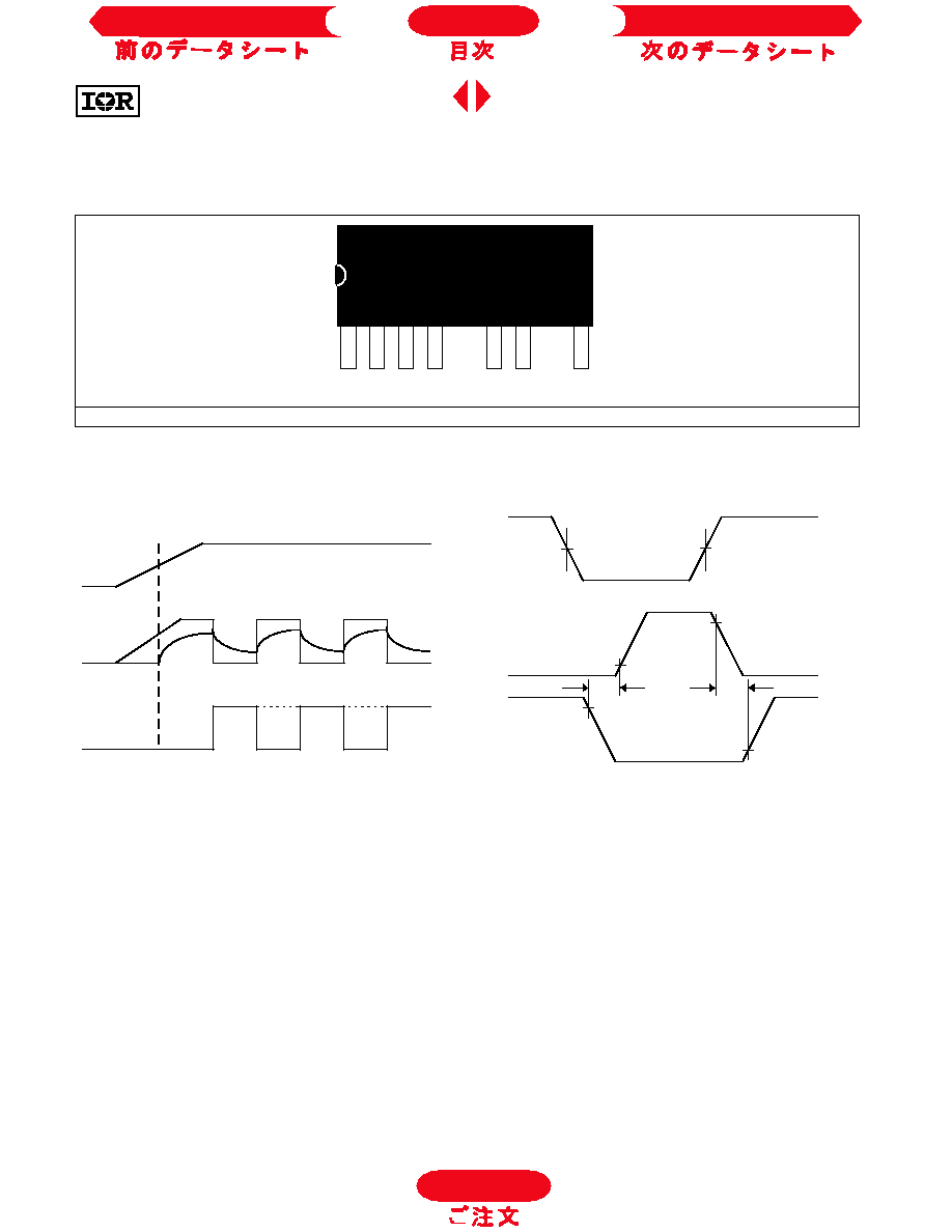
Recommended Operating Conditions
The Input/Output logic timing diagram is shown in Figure 1. For proper operation the device should be used
within the recommended conditions.
Parameter
Symbol
Definition
Min.
Max.
Units
V
B
High Side Floating Supply Absolute Voltage
VO + 10
VO + V
CLAMP
V
IN
High Voltage Supply
---
250
V
VO
Half-Bridge Output Voltage
---
250
I
D
Continuous Drain Current
(T
A
=
25ºC)
---
0.85
A
(T
A
=
85ºC)
---
0.55
I
CC
Supply Current (Note 1)
---
5
mA
T
A
Ambient Temperature
-40
125
ºC
Note 1:
Because of the IR51HD214's application specificity toward off-line supply systems, this IC contains a
zener clamp structure between the chip V
CC
and COM which has a nominal breakdown voltage of
15.6V. Therefore, the IC supply voltage is normally derived by current feeding the V
CC
lead
(typically by means of a high value resistor connected between the chip V
CC
and the rectified line
voltage and a local decoupling capacitor from V
CC
to COM) and allowing the internal zener clamp
circuit to determine the nominal supply voltage. Therefore, this circuit should not be driven by a DC,
low impedance power source of greater than V
CLAMP
.
Next Data Sheet
Index
Previous Datasheet
To Order
IR51HD214
Dynamic Electrical Characteristics
V
BIAS
(V
CC
, V
B
) = 12V unless otherwise specified.
Parameter
T
A
= 25ºC
Symbol
Definition
Min.
Typ. Max. Units
Test Conditions
t
rr
Reverse Recovery Time (MOSFET Body Diode)
---
190
---
ns
I
F
= 850mA
Q
rr
Reverse Recovery Charge (MOSFET Body Diode)
---
0.64
---
µC
di/dt = 100A/µs
DT
Deadtime, LS Turn-Off to HS Turn-On &
HS Turn-Off to LS Turn-On
---
1.2
---
µs
D
R
T
Duty Cycle
---
50
---
%
f
OSC
= 20 kHz
Static Electrical Characteristics
V
BIAS
(V
CC
, V
B
) = 12V unless otherwise specified.
Parameter
T
A
= 25ºC
Symbol
Definition
Min.
Typ. Max. Units
Test Conditions
Supply Characteristics
V
CCUV+
V
CC
Supply Undervoltage Positive Going
Threshold
---
8.4
---
V
V
CCUV-
V
CC
Supply Undervoltage Negative Going
Threshold
---
8.0
---
I
QCC
Quiescent V
CC
Supply Current
---
300
---
µA
V
CLAMP
V
CC
Zener Shunt Clamp Voltage
---
15.6
---
V
I
CC
= 5 mA
Floating Supply Characteristics
I
QBS
Quiescent V
BS
Supply Current
---
30
---
µA
I
OS
Offset Supply Leakage Current---
---
50
V
B
= V
IN
= 250V
Oscillator I/O Characteristics
f
OSC
Oscillator Frequency
---
20
---
kHz
R
T
= 35.7 k
,
C
T
= 1 nF
---
100
---
R
T
= 7.04 k
,
C
T
= 1 nF
I
CT
C
T
Input Current
---
0.001
1.0
µA
V
CTUV
C
T
Undervoltage Lockout
---
100
---
2.5V < V
CC
< V
CCUV+
V
RT+
R
T
High Level Output Voltage, V
CC
- R
T
---
20
---
I
RT
= -100 µA
---
200
---
mV
I
RT
= -1 mA
V
RT-
R
T
Low Level Output Voltage
---
20
---
I
RT
= 100 µA
---
200
---
I
RT
= 1 mA
V
RTUV
R
T
Undervoltage Lockout, V
CC
- R
T
---
100
---
2.5V < V
CC
< V
CCUV+
V
CT+
2/3 V
CC
Threshold
---
8.0
---
V
V
CT-
1/3 V
CC
Threshold
---
4.0
---
Output Characteristics
R
DS(on)
Static Drain-to-Source On-Resistance
---
2.0
---
I
D
= 850mA
V
SD
Diode Forward Voltage
---
0.8
---
V
T
j
= 150 ºC
To Order
Next Data Sheet
Index
Previous Datasheet
IR51HD214
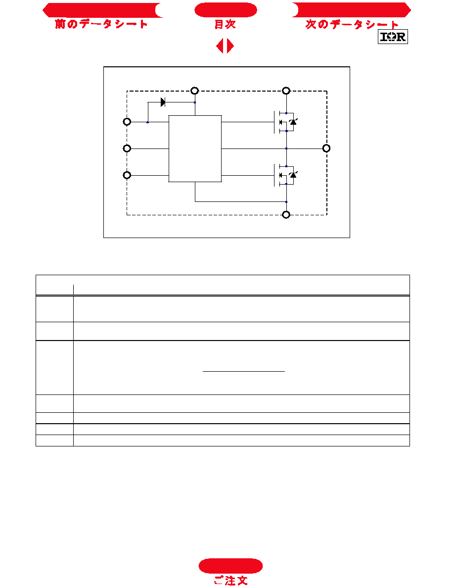
Functional Block Diagram
IR2151
VO
COM
V
B
V
CC
VIN
IRFC214
IRFC214
1
2
3
4
6
9
7
R
T
C
T
Lead Definitions
Lead
Symbol
Description
V
CC
Logic and internal gate drive supply voltage. An internal zener clamp diode at 15.6 V nominal is
included to allow the Vcc to be current fed directly from V
IN
typically by means of a high value
resistor.
R
T
Oscillator timing resistor input; a resistor is connected from R
T
to C
T
. R
T
is out of phase with
the half-bridge output (VO).
C
T
Oscillator timing capacitor output; a capacitor is connected from C
T
to COM in order to program
the oscillator frequency according to the following equation:
f
=
+
1
1 4
R
75
C
T
T
. × (
) ×
where 75
is the effective impedance of the R
T
output stage.
V
B
High side gate drive floating supply. For bootstrap operation a high voltage fast recovery diode is
needed to feed from V
CC
to V
B
.
V
IN
High voltage supply.
VO
Half-bridge output.
COM
Logic and low side of half-bridge return.
To Order
Next Data Sheet
Index
Previous Datasheet
IR51HD214
Lead Assignments
V
CC
V0
VIN
R
C
COM
V
B
9
7
6
4
3
2
1
T
T
9 Lead SIP w/o Leads 5 & 8
IR51HD214
VO
V
CC
V
CLAMP
V
CCUV
+
R
T
C
T
V+
0
R
T
HIGH
SIDE
50%
50%
90%
10%
LOW
SIDE
90%
10%
DT
Figure 1. Input/Output Timing Diagram
Figure 2. Deadtime Waveform Definitions
To Order
Next Data Sheet
Index
Previous Datasheet