1
®
FN8239.1
CAUTION: These devices are sensitive to electrostatic discharge; follow proper IC Handling Procedures.
1-888-INTERSIL or 321-724-7143
|
Intersil (and design) is a registered trademark of Intersil Americas Inc.
Copyright Intersil Americas Inc. 2005. All Rights Reserved
All other trademarks mentioned are the property of their respective owners.
ISL88694
SMBus Accelerator (SMA)
The ISL88694 SMBus accelerator (SMA) is a dual active
pull-up bus terminator designed to improve data
transmission speed on SMBus or similar 2-wire serial bus
interfaces. The ISL88694 is also compatible to the I
2
C serial
bus.
The SMA detects rising input transitions with two internal
voltage references and two comparators per channel. After
the voltage on a data line crosses the first threshold
(V
TRIPL
), the boost pull-up current source is activated to
speed transition. After the voltage crosses the second
threshold (V
TRIPH
), the boost pull-up current source is de-
activated, leaving an active pull-up current of 275µA on the
line. When both channels are HIGH, the pull-up current for
both lines is reduced to 100µA to save power. Internal logic
ensures that the active and boost pull-up current sources are
not activated during downward transitions.
The level for V
TRIPH
is controlled by a bandgap voltage
referred to V
DD
. This feature makes the switching behavior
invariant for all power supply voltages between 2.7V and
5.5V.
A noise filter on each channel prevents the circuit from
responding to input transitions that do not exceed a voltage-
time threshold. To activate the boost circuit, the input must
exceed V
TRIPL
by 100Vns (typical) (See Figure 10).
The SMA permits operation of the bus at frequencies up to
100kHz, despite the capacitive loads of multiple devices
and/or long PC board traces. Enhanced ESD protection on
the accelerator pins are guaranteed to withstand 8kV ESD
(HBM) events.
The SMBus Accelerator provides an essential function in
SMBus applications because of distributed capacitance of
SMBus and multiple device input capacitances at various
nodes. By incorporating SMA, systems using SMBus or I
2
C
can reliably increase their bus load without the risk of data
loss.
Features
· Active Termination for SMBus lines
· Enhances System Bus Signal Rise Time
· Increases Bus Capacity While Guaranteeing Data Integrity
· 2.2mA Rise Time Supply Current
· 8kV ESD Protection on SDA and SCL Pins
· Wide Operating Voltage Range: 2.7V to 5.5V
· 2-Wire SMBus and I
2
C Compatible (100kHz)
· Small Package - SOT23-5
· Pin-for-Pin Compatible with the LTC1694
· Pb-Free Available (RoHS Compliant)
Target Applications
· Servers
· Data Acquisition
· Routers
· Battery Chargers
· Portable Instrumentation
· Notebook
· PC
· Facilities Tracking System
Pinout
ISL88694
(5 LD SOT-23)
TOP VIEW
Ordering Information
PART NUMBER
PACKAGE
TEMP RANGE (°C)
ISL88694IH5
5-pin SOT
-40 to 85
ISL88694IH5Z (Note) 5-pin SOT (Pb-Free)
-40 to 85
Add "-TK" suffix for tape and reel.
NOTE: Intersil Pb-free products employ special Pb-free material
sets; molding compounds/die attach materials and 100% matte tin
plate termination finish, which are RoHS compliant and compatible
with both SnPb and Pb-free soldering operations. Intersil Pb-free
products are MSL classified at Pb-free peak reflow temperatures that
meet or exceed the Pb-free requirements of IPC/JEDEC J STD-020.
V
DD
1
2
3
4
5
N.C.
SMBus1
GND
SMBus2
Data Sheet
January 21, 2005
3
FN8239.1
January 21, 2005
Absolute Maximum Ratings
Recommended Operating Conditions
Supply Voltage Range . . . . . . . . . . . . . . . . . . . . . . . . . . . -1V to 6.5V
Operating Junction Temperature . . . . . . . . . . . . . . . . . . . . . . +135°C
Storage Temperature Range . . . . . . . . . . . . . . . . . .-65°C to +150°C
Voltage on pins . . . . . . . . . . . . . . . . . . . . . . . . . . -0.3V to V
DD
+0.3V
Lead temperature (soldering, 10 seconds) . . . . . . . . . . . . . . . 300°C
ESD min other pins (HBM). . . . . . . . . . . . . . . . . . . . . . . . . . . . .>2kV
ESD SMBus1 and SMBus2 pins (HBM) . . . . . . . . . . . . . . . . . .>8kV
Temperature . . . . . . . . . . . . . . . . . . . . . . . . . . . . . . .-40°C to +85°C
Supply Voltage. . . . . . . . . . . . . . . . . . . . . . . . . . . . . . . . 2.7V to 5.5V
CAUTION: Absolute Maximum Ratings indicate limits beyond which permanent damage to the device and impaired reliability may occur. These are stress ratings
provided for information only and functional operation of the device at these or any other conditions beyond those indicated in the operational sections of this
specification are not implied.
For guaranteed specifications and test conditions, see Electrical Specifications. The guaranteed specifications apply only for the test conditions listed. Some
performance characteristics may degrade when the device is not operated under the listed test conditions.
Electrical Specifications
Over operating conditions unless otherwise specified, Typical values are measured at V
DD
= 3.3V and
T
A
= +25°C
SYMBOL
PARAMETER
CONDITIONS
MIN
TYP
MAX
UNIT
ANALOG PARAMETERS
V
DD
Supply Voltage Range
2.7
5.5
V
V
DD RAMP
V
DD
Ramp Rate
0.05
50
V/msec
I
DD
Supply Current
SMBus1=SMBus2=Open
80
100
µA
I
OUT_SB
Standby Pull-Up Current
SMBus1=SMBus2=V
DD
-1.0V
80
125
µA
I
OUT_A1
Active Pull-Up Current
SMBus1=GND; SMBus2=Open
125
275
350
µA
I
OUT_A2
SMBus1= Open; SMBus2=GND
125
275
350
µA
I
OUT_B1
Boost Pull-Up Current (Figure 1) V
TRIPL
<SMBus1<V
TRIPH
, SMBus2=Open
1.6
2.2
mA
I
OUT_B2
V
TRIPL
<SMBus2<V
TRIPH
, SMBus1=Open
1.6
2.2
mA
V
TRIPL
Input Voltage Threshold Low
0.65
0.75
0.85
V
V
TRIPH
Input Voltage Threshold High
V
DD
-0.60
V
DD
- 0.50
V
DD
- 0.40
V
f
MAX
SMBus Max Frequency
100
kHz
NSS
Noise Spike Suppression
(Note 1) (Figure 10)
20
V-nsec
NOTES:
1. Measured as area under triangular waveform above V
TRIPL
, with time as base and V
IN
as height (See Figure 10).
ISL88694
5
FN8239.1
January 21, 2005
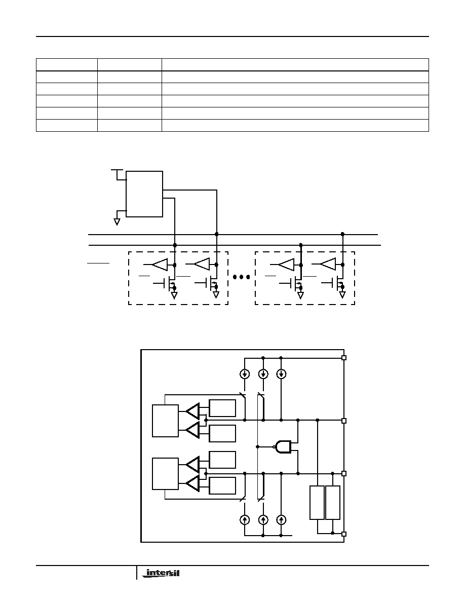
Functional Description
SMBus Overview
The SMBus or I
2
C bus is a 2-wire multimaster bus, meaning
that more than one device connected to the bus is capable of
controlling it. Master devices communicate to other master
or slave devices using one clock and one data line. These
are both bidirectional.
In order to allow multimaster operation without bus
contention, it is necessary to allow each bus to be connected
to a positive supply voltage via a current-source or pull-up
resistor (see "System Diagram" on page 2). When the bus is
free, both lines are HIGH. The output stages of devices
connected to the bus must have an open-drain or open-
collector to perform the wired-AND function.
Simple pull-up resistors on the clock and data lines work well
unless there are long signal lines or many devices
connected to the bus. Then, the combined capacitance of
the bus increases the rise time on the signal to such an
extent that the communication becomes unreliable or fails to
meet the bus timing specifications. Smaller resistors can
sometimes compensate for the extra capacitance, but this
increases the current consumption when the signal lines are
pulled LOW.
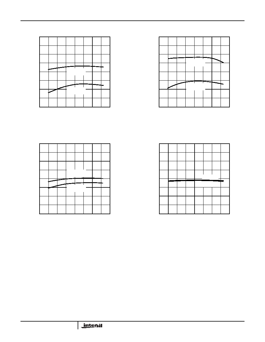
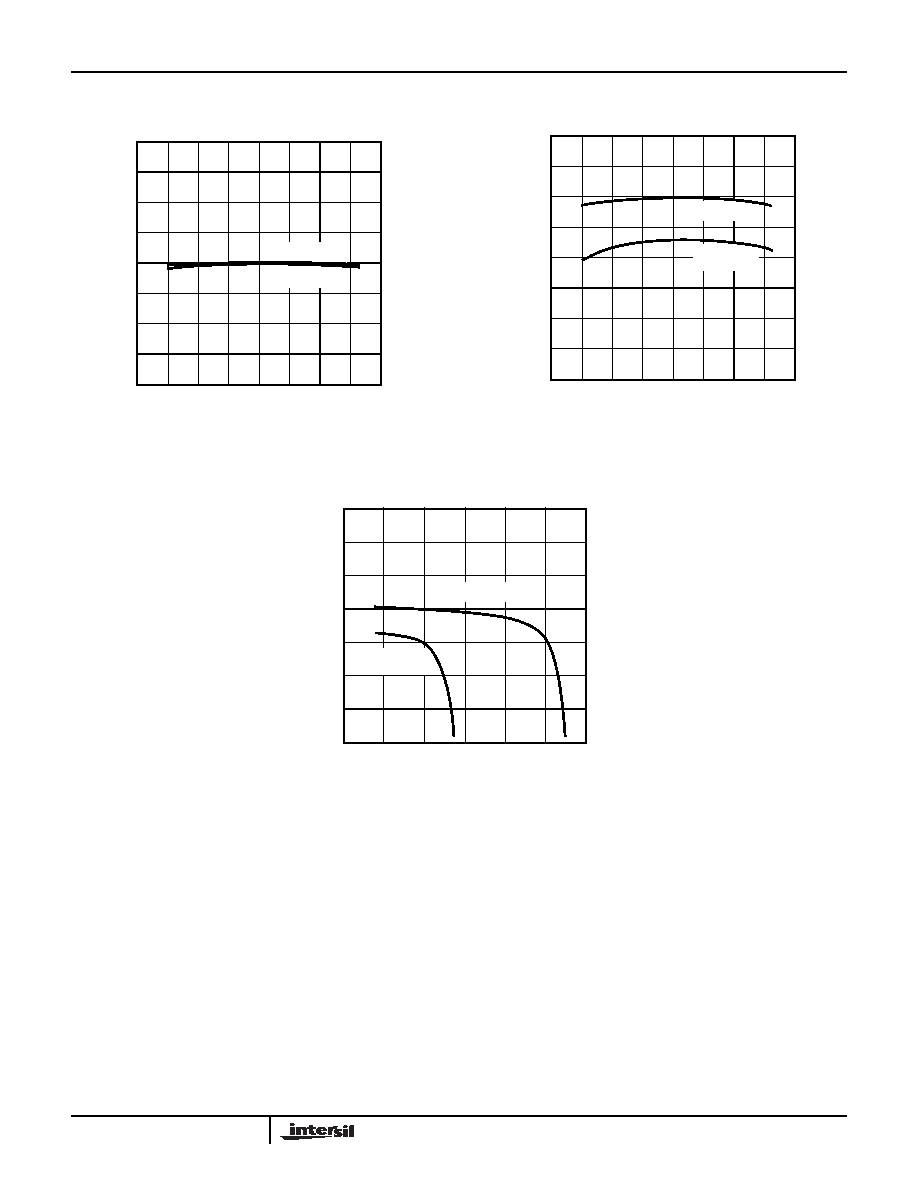
FIGURE 5. V
TRIPH
VOLTAGE
FIGURE 6. I
DD
CURRENT. SMBus1=SMBus2=OPEN.
FIGURE 7. BOOST PULL-UP CURRENT vs. SMBus VOLTAGE
Typical Performance Curves
(Continued)
0.50
0.55
0.60
0.65
0.70
0.45
0.40
0.35
0.30
-40
-20
0
20
40
60
80
100
-60
TEMPERATURE (°C)
IN
P
U
T
THRESHOL
D HIGH, V
TR
IPH
(V
DD
-V)
VDD=5.5V
VDD=2.7V
75
80
85
90
95
70
65
60
55
-40
-20
0
20
40
60
80
100
-60
TEMPERATURE (°C)
S
U
P
P
L
Y
C
URRENT
,
I
DD
(µA)
VDD=5.5V
VDD=2.7V
2.0
2.5
3.0
3.5
1.5
1.0
0.5
0
1
2
3
4
5
0
SMBus VOLTAGE (V)
BOOST PULL-UP CU
RRE
N
T
,
I
OU
T
_
B
(mA)
6
VDD=5.0V
VDD=2.7V
ISL88694