 | –≠–ª–µ–∫—Ç—Ä–æ–Ω–Ω—ã–π –∫–æ–º–ø–æ–Ω–µ–Ω—Ç: ISL6753 | –°–∫–∞—á–∞—Ç—å:  PDF PDF  ZIP ZIP |
1
Æ
ISL6753
ZVS Full-Bridge PWM Controller
The ISL6753 is a high-performance, low-pin-count
alternative zero-voltage switching (ZVS) full-bridge PWM
controller. Like the ISL6551, it achieves ZVS operation by
driving the upper bridge FETs at a fixed 50% duty cycle while
the lower bridge FETS are trailing-edge modulated with
adjustable resonant switching delays. Compared to the more
familiar phase-shifted control method, this algorithm offers
equivalent efficiency and improved overcurrent and light-
load performance with less complexity in a lower pin count
package.
This advanced BiCMOS design features low operating
current, adjustable oscillator frequency up to 2MHz,
adjustable soft-start, internal over temperature protection,
precision deadtime and resonant delay control, and short
propagation delays. Additionally, Multi-Pulse Suppression
ensures alternating output pulses at low duty cycles where
pulse skipping may occur.
Features
∑ Adjustable Resonant Delay for ZVS Operation
∑ Voltage- or Current-Mode Operation
∑ 3% Current Limit Threshold
∑
175
µA Startup Current
∑ Supply UVLO
∑ Adjustable Deadtime Control
∑ Adjustable Soft-Start
∑ Adjustable Oscillator Frequency Up to 2MHz
∑ Tight Tolerance Error Amplifier Reference Over Line,
Load, and Temperature
∑ 5MHz GBWP Error Amplifier
∑ Adjustable Cycle-by-Cycle Peak Current Limit
∑ Fast Current Sense to Output Delay
∑ 70ns Leading Edge Blanking
∑ Multi-Pulse Suppression
∑ Buffered Oscillator Sawtooth Output
∑ Internal Over Temperature Protection
∑ Pb-free and ELV, WEEE, RoHS Compliant
Applications
∑ ZVS Full-Bridge Converters
∑ Telecom and Datacom Power
∑ Wireless Base Station Power
∑ File Server Power
∑ Industrial Power Systems
Ordering Information
PART NUMBER
TEMP. RANGE
(∞C)
PACKAGE
PKG.
DWG. #
ISL6753AAZA
(See Note)
-40 to 105
16 Ld QSOP
(Pb-free)
M16.15A
Add -T suffix to part number for tape and reel packaging
NOTE: Intersil Pb-free products employ special Pb-free material
sets; molding compounds/die attach materials and 100% matte tin
plate termination finish, which are RoHS compliant and compatible
with both SnPb and Pb-free soldering operations. Intersil Pb-free
products are MSL classified at Pb-free peak reflow temperatures that
meet or exceed the Pb-free requirements of IPC/JEDEC J STD-020.
Pinout
ISL6753 (QSOP)
TOP VIEW
RTD
SS
CT
OUTUR
OUTUL
CTBUF
OUTLR
RESDEL
RAMP
OUTLL
FB
VDD
VERR
VREF
CS
GND
1
2
4
3
5
6
7
8
9
10
11
12
13
14
15
16
Data Sheet
March 10, 2005
FN9182.1
CAUTION: These devices are sensitive to electrostatic discharge; follow proper IC Handling Procedures.
1-888-INTERSIL or 1-888-352-6832
|
Intersil (and design) is a registered trademark of Intersil Americas Inc.
Copyright Intersil Americas Inc. 2005. All Rights Reserved
All other trademarks mentioned are the property of their respective owners.
2
FN9182
.1
March
10, 200
5
ISL6753
Functional Block Diagram
OUTLL
OUTLR
OUTUL
OUTUR
VDD
PWM
STEERING
LOGIC
RESDEL
UVLO
OVER-
TEMPERATURE
PROTECTION
VREF
OSCILLATOR
CT
RTD
VDD
GND
VREF
RAMP
+
-
+
-
0.6V
0.33
80mV
VREF
SOFTSTART
CONTROL
VREF
50%
PWM
VERR
FB
1 mA
SS
CTBUF
CS
PWM
COMPARATOR
+
-
1.00V
OVER CURRENT
COMPARATOR
70 nS
LEADING
EDGE
BLANKING

3
FN9182
.1
March
10, 200
5
ISL6753
Typical Application - High Voltage Input ZVS Full-Bridge Converter
P1
VIN+
P2
VIN-
P4
RETURN
T2
P8205
R7A, B
18.7
0805
C8
1.0nF
C9
0.47uF
C18
1uF
100V
1210
C5
0.1uF
R1
4.7k
5%
2512
R3
4.7k
5%
2512
R2
4.7k
5%
2512
Q11
MJD50
300 - 400
VDC
U1
ISL6753
L1
PB2020.103
T1
R5
100k
1206
VR1
BZX84-C12
R8
45.3k
P3
+ Vout
(48V@10A)
C19
1uF
100V
1210
C20
470uF
63V
C21
470uF
63V
C1-C4
33uF
450V
Q2
FQB6N50
Q3
FQB6N50
R11
3.65k
R10
10.0k
R18
10
5%
2512
R19
10
2512
C10
0.1uF
C6
180pF
5% COG
C13
0.1uF
C15
220pF
C16
100pF
250V
COG
T3
P0544
CR4
SS12
CR3
SS12
CR5
CSD10060G
CR6
CSD10060G
+
+
+
Q8
ZXTDB2M832
Q7
ZXTDB2M832
R21
3.74k
1206
R23
1.10k
C14
4.7nF
C17
100pF
250V
COG
U3
R25
37.4k
0805
R20
499
R24
100k
Q9
ZXTDB2M832
Q10
ZXTDB2M832
U2
PS2701-1P
CR1
BAV70
Q1
FQB6N50
Q4
FQB6N50
R4
4.7k
5%
2512
R6
5.11k
R9
499
C7
47pF
RTD
SS
CT
OUTUR
OUTUL
CTBUF
OUTLR
RESDEL
RAMP
OUTLL
FB1
VDD
VERR
VREF
CS
GND
R12
20.0k
Q6
BSS138LT1
Q5
BSS138LT1
Np
Ns
Ns
R13
10.0k
R14
4.99
0805
R15
4.99
0805
R16
10.0k
R17
10.0
R26
10.0k
0805
C11
0.1uF
C12
1.0uF
R28
10.0k
2512
VR2
BZX84-C6V8
+
+
+
CR2
BAT54C
1
2
3
1
2
3
3
1
3
2
1
7
8
3
1
6
3
4
5
8
1
3
1
4
2
5,6
7,8
3
1
4
2
5,6
7,8
3
1
4
2
5,6
7,8
3
1
4
2
5,6
7,8
3
2
1
4
2
3
1
1
3
2
3
1
2
3
1
2
2
1,C
1,C
R27
10.0k
0805
R22
3.74k
1206
C22
4700pF
250VAC
SAFETY
C23
4700pF
250VAC
SAFETY
R29
20.0k
R30
20.0k
2, 3
6, 7
13, 14
11, 12
9, 10
15, 16
CR7
BAT54
3
1
2
BIAS

4
FN9182.1
March 10, 2005
Absolute Maximum Ratings
Thermal Information
Supply Voltage, VDD . . . . . . . . . . . . . . . . . . . GND - 0.3V to +20.0V
OUTxxx . . . . . . . . . . . . . . . . . . . . . . . . . . . . . . . GND - 0.3V to VDD
Signal Pins . . . . . . . . . . . . . . . . . . . . . . . GND - 0.3V to V
REF
+ 0.3V
VREF . . . . . . . . . . . . . . . . . . . . . . . . . . . . . . . . . GND - 0.3V to 6.0V
Peak GATE Current . . . . . . . . . . . . . . . . . . . . . . . . . . . . . . . . . . 0.1A
ESD Classification
Human Body Model (Per MIL-STD-883 Method 3015.7) . . .3000V
Charged Device Model (Per EOS/ESD DS5.3, 4/14/93) . . .1000V
Operating Conditions
Temperature Range
ISL6753AAxx . . . . . . . . . . . . . . . . . . . . . . . . . . .-40∞C to 105∞C
Supply Voltage Range (Typical). . . . . . . . . . . . . . . . . . . . 9-16 VDC
Thermal Resistance Junction to Ambient (Typical)
JA
(∞C/W)
16 Lead QSOP (Note 1). . . . . . . . . . . . . . . . . . . . . .
95
Maximum Junction Temperature . . . . . . . . . . . . . . . . -55∞C to 150∞C
Maximum Storage Temperature Range . . . . . . . . . . . -65∞C to 150∞C
Maximum Lead Temperature (Soldering 10s) . . . . . . . . . . . . . 300∞C
(QSOP- Lead Tips Only)
CAUTION: Stresses above those listed in "Absolute Maximum Ratings" may cause permanent damage to the device. This is a stress only rating and operation of the
device at these or any other conditions above those indicated in the operational sections of this specification is not implied.
NOTES:
1.
JA
is measured with the component mounted on a high effective thermal conductivity test board in free air. See Tech Brief TB379 for details.
2. All voltages are with respect to GND.
Electrical Specifications
Recommended operating conditions unless otherwise noted. Refer to Block Diagram and Typical Application
schematic. 9 V < VDD< 20 V, RTD = 10.0k
, CT = 470pF, T
A
= -40
∞C
to 105
∞C
(Note 3), Typical values are at
T
A
= 25
∞C
PARAMETER
TEST CONDITIONS
MIN
TYP
MAX
UNITS
SUPPLY VOLTAGE
Supply Voltage
-
-
20
-
Start-Up Current, IDD
VDD = 5.0V
-
175
400
µA
Operating Current, IDD
R
LOAD
, C
OUT
= 0
-
11.0
15.5
mA
UVLO START Threshold
8.00
8.75
9.00
V
UVLO STOP Threshold
6.50
7.00
7.50
V
Hysteresis
-
1.75
-
V
REFERENCE VOLTAGE
Overall Accuracy
I
VREF
= 0 - -10mA
4.850
5.000
5.150
V
Long Term Stability
T
A
= 125∞C, 1000 hours (Note 4)
-
3
-
mV
Operational Current (source)
-10
-
-
mA
Operational Current (sink)
5
-
-
mA
Current Limit
VREF = 4.85V
-15
-
-100
mA
CURRENT SENSE
Current Limit Threshold
VERR = VREF
0.97
1.00
1.03
V
CS to OUT Delay
Excl. LEB (Note 4)
-
35
50
ns
Leading Edge Blanking (LEB) Duration
(Note 4)
50
70
100
ns
CS to OUT Delay + LEB
T
A
= 25∞C
-
-
130
ns
CS Sink Current Device Impedance
V
CS
= 1.1V
-
-
20
Input Bias Current
V
CS
= 0.3V
-1.0
-
1.0
µA
RAMP
RAMP Sink Current Device Impedance
V
RAMP
= 1.1V
-
-
20
RAMP to PWM Comparator Offset
T
A
= 25∞C
65
80
95
mV
ISL6753

5
FN9182.1
March 10, 2005
Bias Current
V
RAMP
= 0.3V
-5.0
-
-2.0
µA
Clamp Voltage
(Note 4)
6.5
-
8.0
V
PULSE WIDTH MODULATOR
Minimum Duty Cycle
VERR < 0.6V
-
-
0
%
Maximum Duty Cycle (per half-cycle)
VERR = 4.20V, V
RAMP
= 0V,
V
CS
= 0V (Note 5)
RTD = 2.00k
, CT = 220pF
RTD = 2.00k
, CT = 470pF
-
-
-
94
97
99
-
-
-
%
Zero Duty Cycle VERR Voltage
0.85
-
1.20
V
VERR to PWM Comparator Input Offset
T
A
= 25∞C
0.7
0.8
0.9
V
VERR to PWM Comparator Input Gain
0.31
0.33
0.35
V/V
Common Mode (CM) Input Range
(Note 4)
0
-
V
SS
V
ERROR AMPLIFIER
Input Common Mode (CM) Range
(Note 4)
0
-
VREF
V
GBWP
(Note 4)
5
-
-
MHz
VERR VOL
I
LOAD
= 2mA
-
-
0.4
V
VERR VOH
I
LOAD
= 0mA
4.20
-
-
V
VERR Pull-Up Current Source
VERR = 2.5V
0.8
1.0
1.3
mA
EA Reference
T
A
= 25∞C
0.594
0.600
0.606
V
EA Reference + EA Input Offset Voltage
0.590
0.600
0.612
V
OSCILLATOR
Frequency Accuracy, Overall
(Note 4)
165
183
201
kHz
-10
+10
%
Frequency Variation with VDD
T
A
= 25∞C, (F
20V
- - F
10V
)/F
10V
-
0.3
1.7
%
Temperature Stability
VDD = 10V, |F
-40∞C
- F
0∞C
|/F
0∞C
|F
0∞C
- F
105∞C
|/F
25∞C
(Note 4)
-
-
4.5
1.5
-
-
%
Charge Current
T
A
= 25∞C
-193
-200
-207
µA
Discharge Current Gain
19
20
23
µA/µA
CT Valley Voltage
Static Threshold
0.75
0.80
0.88
V
CT Peak Voltage
Static Threshold
2.75
2.80
2.88
V
CT Pk-Pk Voltage
Static Value
1.92
2.00
2.05
V
RTD Voltage
1.97
2.00
2.03
V
RESDEL Voltage Range
0
-
2
V
CTBUF Gain (V
CTBUFp-p
/V
CTp-p
)
V
CT
= 0.8V, 2.6V
1.95
2.0
2.05
V/V
CTBUF Offset from GND
V
CT
= 0.8V
0.34
0.40
0.44
V
CTBUF VOH
V(I
LOAD
= 0mA, I
LOAD
= -2mA),
V
CT
= 2.6V
-
-
0.10
V
CTBUF VOL
V(I
LOAD
= 2mA, I
LOAD
= 0mA),
V
CT
= 0.8V
-
-
0.10
V
Electrical Specifications
Recommended operating conditions unless otherwise noted. Refer to Block Diagram and Typical Application
schematic. 9 V < VDD< 20 V, RTD = 10.0k
, CT = 470pF, T
A
= -40
∞C
to 105
∞C
(Note 3), Typical values are at
T
A
= 25
∞C (Continued)
PARAMETER
TEST CONDITIONS
MIN
TYP
MAX
UNITS
ISL6753

6
FN9182.1
March 10, 2005
SOFT-START
Charging Current
SS = 3V
-60
-70
-80
µA
SS Clamp Voltage
4.410
4.500
4.590
V
SS Discharge Current
SS = 2V
10
-
-
mA
Reset Threshold Voltage
T
A
= 25∞C
0.23
0.27
0.33
V
OUTPUTS
High Level Output Voltage (VOH)
I
OUT
= -10mA, VDD - VOH
-
0.5
1.0
V
Low Level Output Voltage (VOL)
I
OUT
= 10mA, VOL - GND
-
0.5
1.0
V
Rise Time
C
OUT
= 220pF, VDD = 15V(Note 4)
-
110
200
ns
Fall Time
C
OUT
= 220pF, VDD = 15V(Note 4)
-
90
150
ns
UVLO Output Voltage Clamp
VDD = 7V, I
LOAD
= 1mA (Note 6)
-
-
1.25
V
THERMAL PROTECTION
Thermal Shutdown
(Note 4)
130
140
150
∞C
Thermal Shutdown Clear
(Note 4)
115
125
135
∞C
Hysteresis, Internal Protection
(Note 4)
-
15
-
∞C
NOTE:
3. Specifications at -40∞C and 105∞C are guaranteed by 25∞C test with margin limits.
4. Guaranteed by design, not 100% tested in production.
5. This is the maximum duty cycle achievable using the specified values of RTD and CT. Larger or smaller maximum duty cycles may be obtained
using other values for these components. See Equations 1 - 5.
6. Adjust VDD below the UVLO stop threshold prior to setting at 7V.
Electrical Specifications
Recommended operating conditions unless otherwise noted. Refer to Block Diagram and Typical Application
schematic. 9 V < VDD< 20 V, RTD = 10.0k
, CT = 470pF, T
A
= -40
∞C
to 105
∞C
(Note 3), Typical values are at
T
A
= 25
∞C (Continued)
PARAMETER
TEST CONDITIONS
MIN
TYP
MAX
UNITS
ISL6753
7
FN9182.1
March 10, 2005
Pin Descriptions
VDD - VDD is the power connection for the IC. To optimize
noise immunity, bypass VDD to GND with a ceramic
capacitor as close to the VDD and GND pins as possible.
Supply voltage under-voltage lock-out (UVLO) start and stop
thresholds track each other resulting in relatively constant
hysteresis.
GND - Signal and power ground connections for this device.
Due to high peak currents and high frequency operation, a
low impedance layout is necessary. Ground planes and
short traces are highly recommended.
VREF - The 5.00V reference voltage output having 3%
tolerance over line, load and operating temperature. Bypass
to GND with a 0.1
µF to 2.2µF low ESR capacitor.
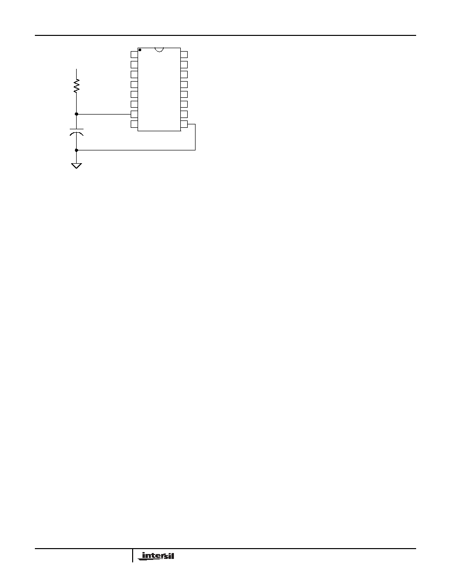
CT - The oscillator timing capacitor is connected between
this pin and GND. It is charged through an internal 200
µA
current source and discharged with a user adjustable current
source controlled by RTD.
RTD - This is the oscillator timing capacitor discharge
current control pin. The current flowing in a resistor
connected between this pin and GND determines the
magnitude of the current that discharges CT. The CT
discharge current is nominally 20x the resistor current. The
PWM deadtime is determined by the timing capacitor
discharge duration. The voltage at RTD is nominally 2.00V.
CS - This is the input to the overcurrent comparator. The
overcurrent comparator threshold is set at 1.00V nominal.
The CS pin is shorted to GND at the termination of either
PWM output.
Depending on the current sensing source impedance, a
series input resistor may be required due to the delay
between the internal clock and the external power switch.
This delay may result in CS being discharged prior to the
power switching device being turned off.
RAMP - This is the input for the sawtooth waveform for the
PWM comparator. The RAMP pin is shorted to GND at the
termination of the PWM signal. A sawtooth voltage
Typical Performance Curves
FIGURE 1. REFERENCE VOLTAGE vs TEMPERATURE
FIGURE 2. CT DISCHARGE CURRENT GAIN vs RTD CURRENT
FIGURE 3. DEADTIME (DT) vs CAPACITANCE
FIGURE 4. CAPACITANCE vs FREQUENCY
40 25 10 5 20 35 50 65 80 95 110
0.98
0.99
1
1.01
1.02
Temperature (C)
Normalized Vref
0
200
400
600
800
1000
18
19
20
21
22
23
24
25
RTD Current (uA)
CT Discharge Current Gain
0
10
20
30
40
50
60
70
80
90 100
10
100
1 .10
3
1 .10
4
RTD (kohms)
D
eadtime - TD
(nS
)
CT =
1000pF
680pF
470pF
330pF
220pF
100pF
0.1
1
10
10
100
1 .10
3
CT (nF)
Fr
equency (
k
Hz)
RTD=
10k
50k
100k
ISL6753

8
FN9182.1
March 10, 2005
waveform is required at this input. For current-mode control
this pin is connected to CS and the current loop feedback
signal is applied to both inputs. For voltage-mode control,
the oscillator sawtooth waveform may be buffered and used
to generate an appropriate signal, RAMP may be connected
to the input voltage through a RC network for voltage feed
forward control, or RAMP may be connected to VREF
through a RC network to produce the desired sawtooth
waveform.
OUTUL and OUTUR - These outputs control the upper
bridge FETs and operate at a fixed 50% duty cycle in
alternate sequence. OUTUL controls the upper left FET and
OUTUR controls the upper right FET. The left and right
designation may be switched as long as they are switched in
conjunction with the lower FET outputs, OUTLL and OUTLR.
RESDEL - Sets the resonant delay period between the
toggle of the upper FETs and the turn on of either of the
lower FETs. The voltage applied to RESDEL determines
when the upper FETs switch relative to a lower FET turning
on. Varying the control voltage from 0 to 2.00V increases the
resonant delay duration from 0 to 100% of the deadtime. The
control voltage divided by 2 represents the percent of the
deadtime equal to the resonant delay. In practice the
maximum resonant delay must be set lower than 2.00V to
ensure that the lower FETs, at maximum duty cycle, are OFF
prior to the switching of the upper FETs.
OUTLL and OUTLR - These outputs control the lower
bridge FETs, are pulse width modulated, and operate in
alternate sequence. OUTLL controls the lower left FET and
OUTLR controls the lower right FET. The left and right
designation may be switched as long as they are switched in
conjunction with the upper FET outputs, OUTUL and
OUTUR.
VERR - The control voltage input to the inverting input of the
PWM comparator. The output of an external error amplifier
(EA) is applied to this input for closed loop regulation. VERR
has a nominal 1mA pull-up current source.
FB - FB is the inverting input to the error amplifier (EA).
SS - Connect the soft-start timing capacitor between this pin
and GND to control the duration of soft-start. The value of
the capacitor determines the rate of increase of the duty
cycle during start up.
SS may also be used to inhibit the outputs by grounding
through a small transistor in an open collector/drain
configuration.
CTBUF - CTBUF is the buffered output of the sawtooth
oscillator waveform present on CT and is capable of
sourcing 2mA. It is offset from ground by 0.40V and has a
nominal valley-to-peak gain of 2. It may be used for slope
compensation.
Functional Description
Features
The ISL6753 PWM is an excellent choice for low cost ZVS
full-bridge applications employing conventional output
rectification. If synchronous rectification is required, please
consider the ISL6752 or ISL6551 products.
With the ISL6753's many protection and control features, a
highly flexible design with minimal external components is
possible. Among its many features are support for both
current- and voltage-mode control, a very accurate
overcurrent limit threshold, thermal protection, a buffered
sawtooth oscillator output suitable for slope compensation,
voltage controlled resonant delay, and adjustable frequency
with precise deadtime control.
Oscillator
The ISL6753 has an oscillator with a programmable
frequency range to 2MHz, and can be programmed with an
external resistor and capacitor.
The switching period is the sum of the timing capacitor
charge and discharge durations. The charge duration is
determined by CT and a fixed 200
µA internal current source.
The discharge duration is determined by RTD and CT.
where T
C
and T
D
are the charge and discharge times,
respectively, T
SW
is the oscillator period, and F
SW
is the
oscillator frequency. One output switching cycle requires two
oscillator cycles. The actual times will be slightly longer than
calculated due to internal propagation delays of
approximately 10nS/transition. This delay adds directly to
the switching duration, but also causes overshoot of the
timing capacitor peak and valley voltage thresholds,
effectively increasing the peak-to-peak voltage on the timing
capacitor. Additionally, if very small discharge currents are
used, there will be increased error due to the input
impedance at the CT pin.
The maximum duty cycle, D, and percent deadtime, DT, can
be calculated from:
T
C
11.5 10
3
CT
S
(EQ. 1)
T
D
0.06 RTD CT
(
)
50 10
9
≠
+
S
(EQ. 2)
T
SW
T
C
T
D
+
1
F
SW
------------
=
=
S
(EQ. 3)
D
T
C
T
SW
------------
=
(EQ. 4)
DT
1 D
≠
=
(EQ. 5)
ISL6753
9
FN9182.1
March 10, 2005
Soft-Start Operation
The ISL6753 features a soft-start using an external capacitor
in conjunction with an internal current source. Soft-start
reduces component stresses and surge currents during start
up.
Upon start up, the soft-start circuitry limits the error voltage
input (VERR) to a value equal to the soft-start voltage. The
output pulse width increases as the soft-start capacitor
voltage increases. This has the effect of increasing the duty
cycle from zero to the regulation pulse width during the soft-
start period. When the soft-start voltage exceeds the error
voltage, soft-start is completed. Soft-start occurs during
start-up and after recovery from a fault condition. The soft-
start charging period may be calculated as follows:
where t is the charging period in mS and C is the value of the
soft-start capacitor in
µF.
The soft-start voltage is clamped to 4.50V with a tolerance of
2%. It is suitable for use as a "soft-started" reference
provided the current draw is kept well below the 70
µA
charging current.
The outputs may be inhibited by using the SS pin as a
disable input. Pulling SS below 0.25V forces all outputs low.
An open collector/drain configuration may be used to couple
the disable signal into the SS pin.
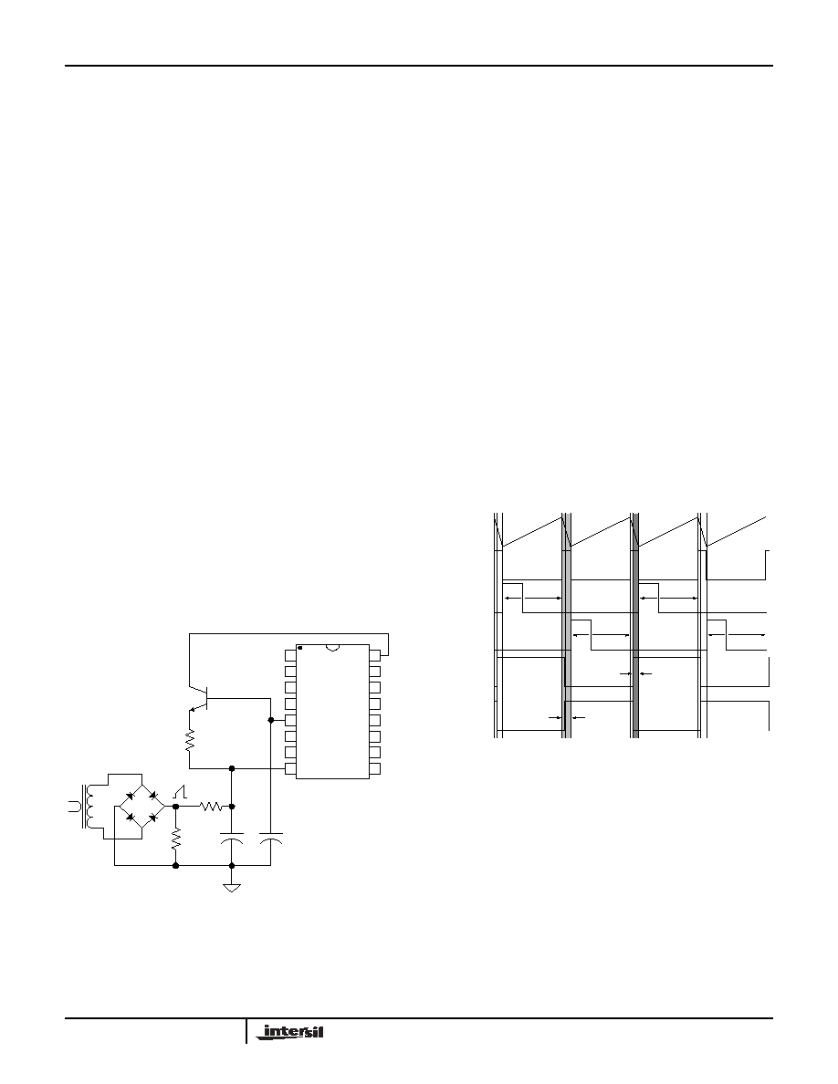
Gate Drive
The ISL6753 outputs are capable of sourcing and sinking
10mA (at rated VOH, VOL) and are intended to be used in
conjunction with integrated FET drivers or discrete bipolar
totem pole drivers. The typical on resistance of the outputs is
50
.
Overcurrent Operation
The cycle-by-cycle peak current limit results in pulse-by-
pulse duty cycle reduction when the current feedback signal
exceeds 1.0V. When the peak current exceeds the
threshold, the active output pulse is immediately terminated.
This results in a decrease in output voltage as the load
current increases beyond the current limit threshold. The
ISL6753 operates continuously in an overcurrent condition
without shutdown.
If voltage-mode control is used in a bridge topology, it should
be noted that peak current limit results in inherently unstable
operation. The DC blocking capacitors used in voltage-mode
bridge topologies become unbalanced, as does the flux in
the transformer core. A latching overcurrent shutdown
method using external components is recommended.
The propagation delay from CS exceeding the current limit
threshold to the termination of the output pulse is increased
by the leading edge blanking (LEB) interval. The effective
delay is the sum of the two delays and is nominally 105nS.
Voltage Feed Forward Operation
Voltage feed forward is a technique used to regulate the
output voltage for changes in input voltage without the
intervention of the control loop. Voltage feed forward is often
implemented in voltage-mode control loops, but is redundant
and unnecessary in peak current-mode control loops.
Voltage feed forward operates by modulating the sawtooth
ramp in direct proportion to the input voltage. Figure 5
demonstrates the concept.
Input voltage feed forward may be implemented using the
RAMP input. An RC network connected between the input
voltage and ground, as shown in Figure 7, generates a
voltage ramp whose charging rate varies with the amplitude
of the source voltage. At the termination of the active output
pulse RAMP is discharged to ground so that a repetitive
sawtooth waveform is created. The RAMP waveform is
compared to the VERR voltage to determine duty cycle. The
selection of the RC components depends upon the desired
input voltage operating range and the frequency of the
oscillator. In typical applications the RC components are
selected so that the ramp amplitude reaches 1.0V at
minimum input voltage within the duration of one half-cycle.
t
64.3 C
=
mS
(EQ. 6)
FIGURE 5. VOLTAGE FEED FORWARD BEHAVIOR
VIN
ERROR VOLTAGE
RAMP
CT
OUTLL, LR
ISL6753
10
FN9182.1
March 10, 2005
The charging time of the ramp capacitor is
For optimum performance, the maximum value of the
capacitor should be limited to 10nF. The maximum DC
current through the resistor should be limited to 2mA
maximum. For example, if the oscillator frequency is
400kHz, the minimum input voltage is 300V, and a 4.7nF
ramp capacitor is selected, the value of the resistor can be
determined by rearranging EQ. 7.
where t is equal to the oscillator period minus the deadtime.
If the deadtime is short relative to the oscillator period, it can
be ignored for this calculation.
If feed forward operation is not desired, the RC network may
be connected to VREF rather than the input voltage.
Alternatively, a resistor divider from CTBUF may be used as
the sawtooth signal. Regardless, a sawtooth waveform must
be generated on RAMP as it is required for proper PWM
operation.
Slope Compensation
Peak current-mode control requires slope compensation to
improve noise immunity, particularly at lighter loads, and to
prevent current loop instability, particularly for duty cycles
greater than 50%. Slope compensation may be
accomplished by summing an external ramp with the current
feedback signal or by subtracting the external ramp from the
voltage feedback error signal. Adding the external ramp to
the current feedback signal is the more popular method.
From the small signal current-mode model [1] it can be
shown that the naturally-sampled modulator gain, Fm,
without slope compensation, is
where Sn is the slope of the sawtooth signal and Tsw is the
duration of the half-cycle. When an external ramp is added,
the modulator gain becomes
where Se is slope of the external ramp and
The criteria for determining the correct amount of external
ramp can be determined by appropriately setting the
damping factor of the double-pole located at half the
oscillator frequency. The double-pole will be critically
damped if the Q-factor is set to 1, and over-damped for Q >
1, and under-damped for Q < 1. An under-damped condition
can result in current loop instability.
where D is the percent of on time during a half cycle. Setting
Q = 1 and solving for Se yields
Since Sn and Se are the on time slopes of the current ramp
and the external ramp, respectively, they can be multiplied
by Ton to obtain the voltage change that occurs during Ton.
where Vn is the change in the current feedback signal during
the on time and Ve is the voltage that must be added by the
external ramp.
Vn can be solved for in terms of input voltage, current
transducer components, and output inductance yielding
where R
CS
is the current sense burden resistor, N
CT
is the
current transformer turns ratio, L
O
is the output inductance,
V
O
is the output voltage, and Ns and Np are the secondary
and primary turns, respectively.
FIGURE 6. VOLTAGE FEED FORWARD CONTROL
VIN
R3
C7
GND
1
2
4
3
5
6
7
8
9
10
11
12
13
14
15
16
RAMP
ISL6753
t
R3 C7
1
V
RAMP PEAK
(
)
V
IN MIN
(
)
----------------------------------------
≠
ln
≠
=
S
(EQ. 7)
R3
t
≠
C7
1
V
RAMP PEAK
(
)
V
IN MIN
)
(
)
----------------------------------------
≠
ln
-------------------------------------------------------------------------
2.5
≠
10
6
≠
4.7 10
9
≠
1
1
300
----------
≠
ln
------------------------------------------------------------
=
=
159
=
k
(EQ. 8)
Fm
1
SnTsw
--------------------
=
(EQ. 9)
Fm
1
Sn Se
+
(
)
Tsw
---------------------------------------
1
m
c
SnTsw
----------------------------
=
=
(EQ. 10)
m
c
1 Se
Sn
-------
+
=
(EQ. 11)
Q
1
m
c
1 D
≠
(
)
0.5
≠
(
)
-------------------------------------------------
=
(EQ. 12
S
e
S
n
1
---
0.5
+
1
1 D
≠
-------------
1
≠
=
(EQ. 13)
V
e
V
n
1
---
0.5
+
1
1 D
≠
-------------
1
≠
=
(EQ. 14)
V
e
T
SW
V
O
R
CS
N
CT
L
O
------------------------------------------
N
S
N
P
--------
1
---
D 0.5
≠
+
=
V
(EQ. 15)
ISL6753

11
FN9182.1
March 10, 2005
The inductor current, when reflected through the isolation
transformer and the current sense transformer to obtain the
current feedback signal at the sense resistor yields
where V
CS
is the voltage across the current sense resistor
and I
O
is the output current at current limit.
Since the peak current limit threshold is 1.00V, the total
current feedback signal plus the external ramp voltage must
sum to this value.
Substituting EQs. 15 and 16 into EQ. 17 and solving for R
CS
yields
For simplicity, idealized components have been used for this
discussion, but the effect of magnetizing inductance must be
considered when determining the amount of external ramp
to add. Magnetizing inductance provides a degree of slope
compensation to the current feedback signal and reduces
the amount of external ramp required. The magnetizing
inductance adds primary current in excess of what is
reflected from the inductor current in the secondary.
where V
IN
is the input voltage that corresponds to the duty
cycle D and Lm is the primary magnetizing inductance. The
effect of the magnetizing current at the current sense
resistor, R
CS
, is
If
V
CS
is greater than or equal to Ve, then no additional
slope compensation is needed and R
CS
becomes
If
V
CS
is less than Ve, then EQ. 18 is still valid for the value
of R
CS
, but the amount of slope compensation added by the
external ramp must be reduced by
V
CS
.
Adding slope compensation is accomplished in the ISL6753
using the CTBUF signal. CTBUF is an amplified
representation of the sawtooth signal that appears on the CT
pin. It is offset from ground by 0.4V and is 2x the peak-to-
peak amplitude of CT (0.4 - 4.4V). A typical application sums
this signal with the current sense feedback and applies the
result to the CS pin as shown in Figure 7.
Assuming the designer has selected values for the RC filter
placed on the CS pin, the value of R9 required to add the
appropriate external ramp can be found by superposition.
Rearranging to solve for R9 yields
The value of R
CS
determined in EQ. 18 must be rescaled so
that the current sense signal presented at the CS pin is that
predicted by EQ. 16. The divider created by R6 and R9
makes this necessary.
Example:
V
IN
= 280V
V
O
= 12V
L
O
= 2.0
µH
Np/Ns = 20
Lm = 2mH
I
O
= 55A
Oscillator Frequency, Fsw = 400kHz
Duty Cycle, D = 85.7%
N
CT
= 50
V
CS
N
S
R
CS
N
P
N
CT
------------------------
I
O
D T
SW
2L
O
---------------------
V
IN
N
S
N
P
--------
V
O
≠
+
=
V
(EQ. 16)
V
e
V
CS
+
1
=
(EQ. 17)
R
CS
N
P
N
CT
N
S
------------------------
1
I
O
V
O
L
O
--------
T
SW
1
---
D
2
----
+
+
------------------------------------------------------
=
(EQ. 18)
I
P
V
IN
DT
SW
L
m
-------------------------------
=
A
(EQ. 19)
V
CS
I
P
R
CS
N
CT
--------------------------
=
V
(EQ. 20)
R
CS
N
CT
N
S
N
P
--------
I
O
DT
SW
2L
O
-----------------
V
IN
N
S
N
P
--------
V
O
≠
+
V
IN
DT
SW
L
m
-------------------------------
+
--------------------------------------------------------------------------------------------------------------------------------------
=
(EQ. 21)
FIGURE 7. ADDING SLOPE COMPENSATION
R6
C4
R9
CTBUF
CS
1
2
4
3
5
6
7
8
R
CS
ISL6753
V
e
V
CS
≠
D V
CTBUF
0.4
≠
(
)
0.4
+
(
)
R6
R6 R9
+
-------------------------------------------------------------------------------
=
V
(EQ. 22)
R9
D V
CTBUF
0.4
≠
(
)
V
e
V
CS
0.4
+
+
≠
(
)
R6
V
e
V
CS
≠
-------------------------------------------------------------------------------------------------------------------
=
(EQ. 23)
R
CS
R6 R9
+
R9
----------------------
R
CS
=
(EQ. 24)
ISL6753
12
FN9182.1
March 10, 2005
R6 = 499
Solve for the current sense resistor, R
CS
, using EQ. 18.
R
CS
= 15.1
.
Determine the amount of voltage, Ve, that must be added to
the current feedback signal using EQ. 15.
Ve = 153mV
Next, determine the effect of the magnetizing current from
EQ. 20.
V
CS
= 91mV
Using EQ. 23, solve for the summing resistor, R9, from
CTBUF to CS.
R9 = 30.1k
Determine the new value of R
CS
, R'
CS
, using EQ. 24.
R'
CS
= 15.4
The above discussion determines the minimum external
ramp that is required. Additional slope compensation may be
considered for design margin.
f the application requires deadtime less than about 500nS,
the CTBUF signal may not perform adequately for slope
compensation. CTBUF lags the CT sawtooth waveform by
300-400nS. This behavior results in a non-zero value of
CTBUF when the next half-cycle begins when the deadtime
is short.
Under these situations, slope compensation may be added
by externally buffering the CT signal as shown below.
Using CT to provide slope compensation instead of CTBUF
requires the same calculations, except that EQs. 21 and 22
require modification. EQ. 21 becomes:
and EQ. 22 becomes:
The buffer transistor used to create the external ramp from
CT should have a sufficiently high gain so as to minimize the
required base current. Whatever base current is required
reduces the charging current into CT and will reduce the
oscillator frequency.
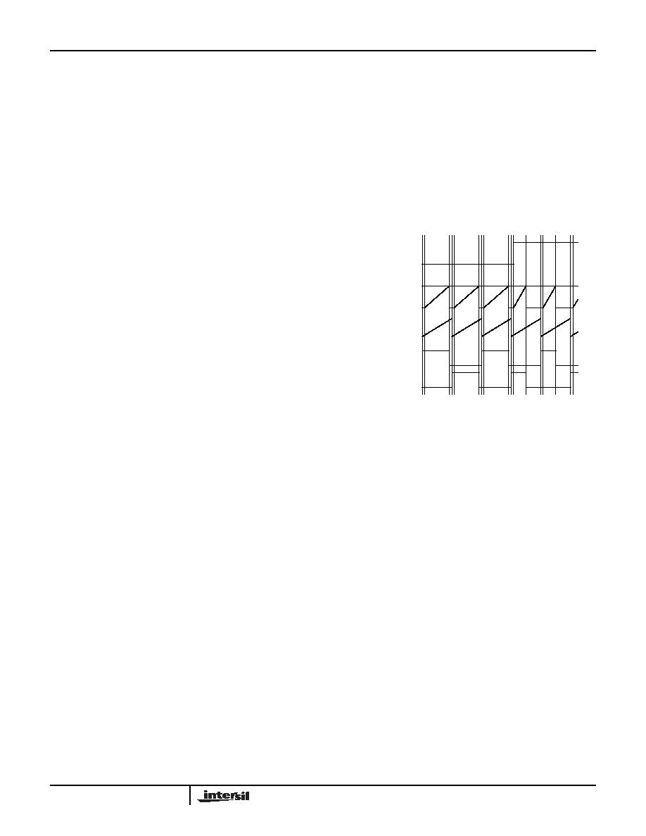
ZVS Full-Bridge Operation
The ISL6753 is a full-bridge zero-voltage switching (ZVS)
PWM controller that behaves much like a traditional hard-
switched topology controller. Rather than drive the diagonal
bridge switches simultaneously, the upper switches (OUTUL,
OUTUR) are driven at a fixed 50% duty cycle and the lower
switches (OUTLL, OUTLR) are pulse width modulated on
the trailing edge.
FIGURE 8. ADDING SLOPE COMPENSATION USING CT
R6
C4
R9
R
CS
CT
CT
CS
1
2
4
3
5
6
7
8
9
10
11
12
13
14
15
16
ISL6753
VREF
V
e
V
CS
≠
2D R6
R6 R9
+
----------------------
=
V
(EQ. 25)
R9
2D V
e
V
CS
+
≠
(
)
R6
V
e
V
CS
≠
-------------------------------------------------------------
=
(EQ. 26)
FIGURE 9. BRIDGE DRIVE SIGNAL TIMING
CT
DEADTIME
OUTLL
OUTLR
OUTUR
OUTUL
RESDEL
WINDOW
RESONANT
DELAY
PWM
PWM
PWM
PWM
ISL6753
13
FN9182.1
March 10, 2005
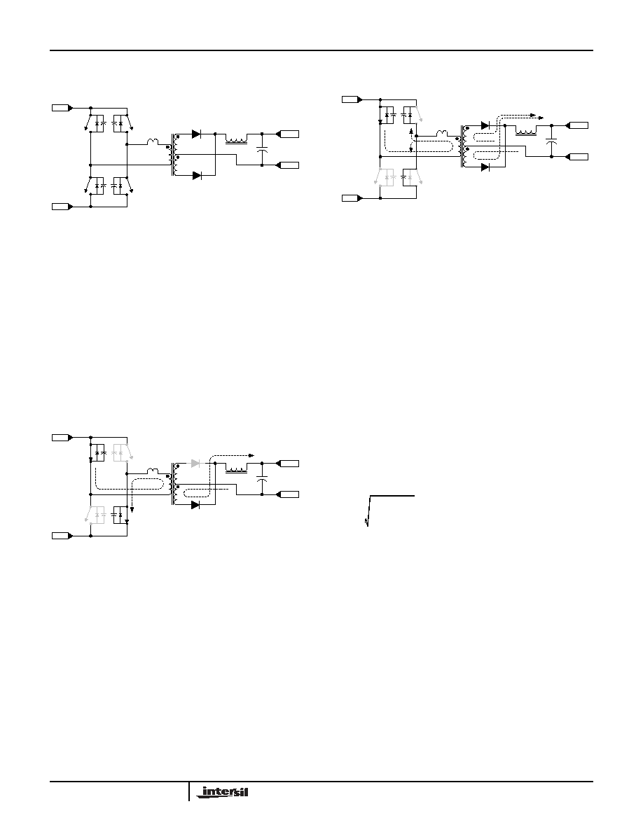
To understand how the ZVS method operates one must
include the parasitic elements of the circuit and examine a
full switching cycle.
In Figure 10, the power semiconductor switches have been
replaced by ideal switch elements with parallel diodes and
capacitance, the output rectifiers are ideal, and the
transformer leakage inductance has been included as a
discrete element. The parasitic capacitance has been
lumped together as switch capacitance, but represents all
parasitic capacitance in the circuit including winding
capacitance. Each switch is designated by its position, upper
left (UL), upper right (UR), lower left (LL), and lower right
(LR). The beginning of the cycle, shown in Figure 11, is
arbitrarily set as having switches UL and LR on and UR and
LL off. The direction of the primary and secondary currents
are indicated by I
P
and I
S
, respectively.
The UL - LR power transfer period terminates when switch
LR turns off as determined by the PWM. The current flowing
in the primary cannot be interrupted instantaneously, so it
must find an alternate path. The current flows into the
parasitic switch capacitance of LR and UR which charges
the node to VIN and then forward biases the body diode of
upper switch UR.
The primary leakage inductance, L
L
, maintains the current
which now circulates around the path of switch UL, the
transformer primary, and switch UR. When switch LR opens,
the output inductor current free-wheels through both output
diodes, D1 and D2. This condition persists through the
remainder of the half-cycle.
During the period when CT discharges, also referred to as
the deadtime, the upper switches toggle. Switch UL turns off
and switch UR turns on. The actual timing of the upper
switch toggle is dependent on RESDEL which sets the
resonant delay. The voltage applied to RESDEL determines
how far in advance the toggle occurs prior to a lower switch
turning on. The ZVS transition occurs after the upper
switches toggle and before the diagonal lower switch turns
on. The required resonant delay is 1/4 of the period of the LC
resonant frequency of the circuit formed by the leakage
inductance and the parasitic capacitance. The resonant
transition may be estimated from EQ. 27.
where
is the resonant transition time, L
L
is the leakage
inductance, C
P
is the parasitic capacitance, and R is the
equivalent resistance in series with L
L
and C
P
.
The resonant delay is always less than or equal to the
deadtime and may be calculated using the following
equation.
where
resdel
is the desired resonant delay, V
resdel
is a
voltage between 0 and 2V applied to the RESDEL pin, and
DT is the deadtime (see EQs. 1 - 5).
When the upper switches toggle, the primary current that
was flowing through UL must find an alternate path. It
charges/discharges the parasitic capacitance of switches UL
and LL until the body diode of LL is forward biased. If
FIGURE 10. IDEALIZED FULL-BRIDGE
VIN+
VIN-
UL
LL
UR
LR
VOUT+
RTN
L
L
D2
D1
FIGURE 11. UL - LR POWER TRANSFER CYCLE
VIN+
VIN-
UL
LL
UR
LR
VOUT+
RTN
I
P
I
S
L
L
D2
D1
FIGURE 12. UL - UR FREE-WHEELING PERIOD
VIN+
VIN-
UL
LL
UR
LR
VOUT+
RTN
I
P
I
S
L
L
D2
D1
2
---
1
1
L
L
C
P
---------------
R
2
4L
L
2
----------
≠
-----------------------------------
=
(EQ. 27)
resdel
V
resdel
2
--------------------
DT
=
S
(EQ. 28)
ISL6753

14
FN9182.1
March 10, 2005
RESDEL is set properly, switch LL will be turned on at this
time.
The second power transfer period commences when switch
LL closes. With switches UR and LL on, the primary and
secondary currents flow as indicated below.
The UR - LL power transfer period terminates when switch
LL turns off as determined by the PWM. The current flowing
in the primary must find an alternate path. The current flows
into the parasitic switch capacitance which charges the node
to VIN and then forward biases the body diode of upper
switch UL. The primary leakage inductance, L
L
, maintains
the current, which now circulates around the path of switch
UR, the transformer primary, and switch UL. When switch LL
opens, the output inductor current free-wheels through both
output diodes, D1 and D2. This condition persists through
the remainder of the half-cycle.
When the upper switches toggle, the primary current that
was flowing through UR must find an alternate path. It
charges/discharges the parasitic capacitance of switches UR
and LR until the body diode of LR is forward biased. If
RESDEL is set properly, switch LR will be turned on at this
time.
The first power transfer period commences when switch LR
closes and the cycle repeats. The ZVS transition requires
that the leakage inductance has sufficient energy stored to
fully charge the parasitic capacitances. Since the energy
stored is proportional to the square of the current (1/2 L
L
I
P
2
,
the ZVS resonant transition is load dependent. If the leakage
inductance is not able to store sufficient energy for ZVS, a
discrete inductor may be added in series with the
transformer primary.
Fault Conditions
A fault condition occurs if VREF or VDD fall below their
undervoltage lockout (UVLO) thresholds or if the thermal
protection is triggered. When a fault is detected, the soft-
start capacitor is quickly discharged, and the outputs are
disabled low. When the fault condition clears and the soft-
start voltage is below the reset threshold, a soft-start cycle
begins.
An overcurrent condition is not considered a fault and does
not result in a shutdown.
Thermal Protection
Internal die over temperature protection is provided. An
integrated temperature sensor protects the device should
the junction temperature exceed 140∞C. There is
approximately 15∞C of hysteresis.
Ground Plane Requirements
Careful layout is essential for satisfactory operation of the
device. A good ground plane must be employed. VDD and
VREF should be bypassed directly to GND with good high
frequency capacitance.
References
[1] Ridley, R., "A New Continuous-Time Model for Current
Mode Control", IEEE Transactions on Power
Electronics, Vol. 6, No. 2, April 1991.
VIN+
VIN-
UL
LL
UR
LR
VOUT+
RTN
L
L
D2
D1
I
S
I
P
FIGURE 13. UPPER SWITCH TOGGLE AND RESONANT
TRANSITION
VIN+
VIN-
UL
LL
UR
LR
VOUT+
RTN
L
L
D2
D1
FIGURE 14. UR - LL POWER TRANSFER
FIGURE 15. UR - UL FREE-WHEELING PERIOD
VIN+
VIN-
UL
LL
UR
LR
VOUT+
RTN
I
P
I
S
L
L
D2
D1
VIN+
VIN-
UL
LL
UR
LR
VOUT+
RTN
I
P
I
S
L
L
D2
D1
FIGURE 16. UPPER SWITCH TOGGLE AND RESONANT
TRANSITION
ISL6753
15
All Intersil U.S. products are manufactured, assembled and tested utilizing ISO9000 quality systems.
Intersil Corporation's quality certifications can be viewed at www.intersil.com/design/quality
Intersil products are sold by description only. Intersil Corporation reserves the right to make changes in circuit design, software and/or specifications at any time without
notice. Accordingly, the reader is cautioned to verify that data sheets are current before placing orders. Information furnished by Intersil is believed to be accurate and
reliable. However, no responsibility is assumed by Intersil or its subsidiaries for its use; nor for any infringements of patents or other rights of third parties which may result
from its use. No license is granted by implication or otherwise under any patent or patent rights of Intersil or its subsidiaries.
For information regarding Intersil Corporation and its products, see www.intersil.com
FN9182.1
March 10, 2005
ISL6753
Shrink Small Outline Plastic Packages (SSOP)
Quarter Size Outline Plastic Packages (QSOP)
NOTES:
1. Symbols are defined in the "MO Series Symbol List" in Section
2.2 of Publication Number 95.
2. Dimensioning and tolerancing per ANSI Y14.5M
-
1982.
3. Dimension "D" does not include mold flash, protrusions or gate
burrs. Mold flash, protrusion and gate burrs shall not exceed
0.15mm (0.006 inch) per side.
4. Dimension "E" does not include interlead flash or protrusions.
Interlead flash and protrusions shall not exceed 0.25mm (0.010
inch) per side.
5. The chamfer on the body is optional. If it is not present, a visual
index feature must be located within the crosshatched area.
6. "L" is the length of terminal for soldering to a substrate.
7. "N" is the number of terminal positions.
8. Terminal numbers are shown for reference only.
9. Dimension "B" does not include dambar protrusion. Allowable
dambar protrusion shall be 0.10mm (0.004 inch) total in excess
of "B" dimension at maximum material condition.
10. Controlling dimension: INCHES. Converted millimeter dimen-
sions are not necessarily exact.
INDEX
AREA
E
D
N
1
2
3
-B-
0.17(0.007)
C A
M
B S
e
-A-
B
M
-C-
A1
A
SEATING PLANE
0.10(0.004)
h x 45∞
C
H
0.25(0.010)
B
M
M
L
0.25
0.010
GAUGE
PLANE
A2
M16.15A
16 LEAD SHRINK SMALL OUTLINE PLASTIC PACKAGE
(0.150" WIDE BODY)
SYMBOL
INCHES
MILLIMETERS
NOTES
MIN
MAX
MIN
MAX
A
0.061
0.068
1.55
1.73
-
A1
0.004
0.0098
0.102
0.249
-
A2
0.055
0.061
1.40
1.55
-
B
0.008
0.012
0.20
0.31
9
C
0.0075
0.0098
0.191
0.249
-
D
0.189
0.196
4.80
4.98
3
E
0.150
0.157
3.81
3.99
4
e
0.025 BSC
0.635 BSC
-
H
0.230
0.244
5.84
6.20
-
h
0.010
0.016
0.25
0.41
5
L
0.016
0.035
0.41
0.89
6
N
16
16
7
0∞
8∞
0∞
8∞
-
Rev. 2 6/04