1
File Number
4766
HIP6302
Microprocessor CORE Voltage Regulator
Multi-Phase Buck PWM Controller
The HIP6302 multi-phase PWM control IC together with its
companion gate drivers, the HIP6601, HIP6602 or HIP6603
and Intersil MOSFETs provides a precision voltage
regulation system for advanced microprocessors.
Multiphase power conversion is a marked departure from
earlier single phase converter configurations previously
employed to satisfy the ever increasing current demands of
modern microprocessors. Multi-phase convertors, by
distributing the power and load current results in smaller and
lower cost transistors with fewer input and output capacitors.
These reductions accrue from the higher effective
conversion frequency with higher frequency ripple current
due to the phase interleaving process of this topology. For
example, a two phase convertor operating at 350kHz will
have a ripple frequency of 700kHz. Moreover, greater
convertor bandwidth of this design results in faster response
to load transients.
Outstanding features of this controller IC include
programmable VID codes from the microprocessor that
range from 1.100V to 1.850V with a system accuracy of
±
1%. Pull up currents on these VID pins eliminates the need
for external pull up resistors. In addition "droop"
compensation, used to reduce the overshoot or undershoot
of the CORE voltage, is easily programmed with a single
resistor.
Another feature of this controller IC is the PGOOD monitor
circuit which is held low until the CORE voltage increases,
during its Soft-Start sequence, to within 10% of the
programmed voltage. Over-voltage, 15% above programmed
CORE voltage, results in the converter shutting down and
turning the lower MOSFETs ON to clamp and protect the
microprocessor. Under voltage is also detected and results
in PGOOD low if the CORE voltage falls 10% below the
programmed level. Over-current protection reduces the
regulator current to less than 25% of the programmed trip
value. These features provide monitoring and protection for
the microprocessor and power system.
Features
∑ Multi-Phase Power Conversion
∑ Precision Channel Current Sharing
- Loss Less Current Sampling - Uses r
DS(ON)
∑ Precision CORE Voltage Regulation
-
±
1% System Accuracy Over Temperature
∑ Microprocessor Voltage Identification Input
- 5-Bit VID Input
- 1.100V to 1.850V in 25mV Steps
- Programmable "Droop" Voltage
∑ Fast Transient Recovery Time
∑ Over Current Protection
∑ High Ripple Frequency, (Channel Frequency) Times
Number Channels . . . . . . . . . . . . . . . . . 100kHz to 3MHz
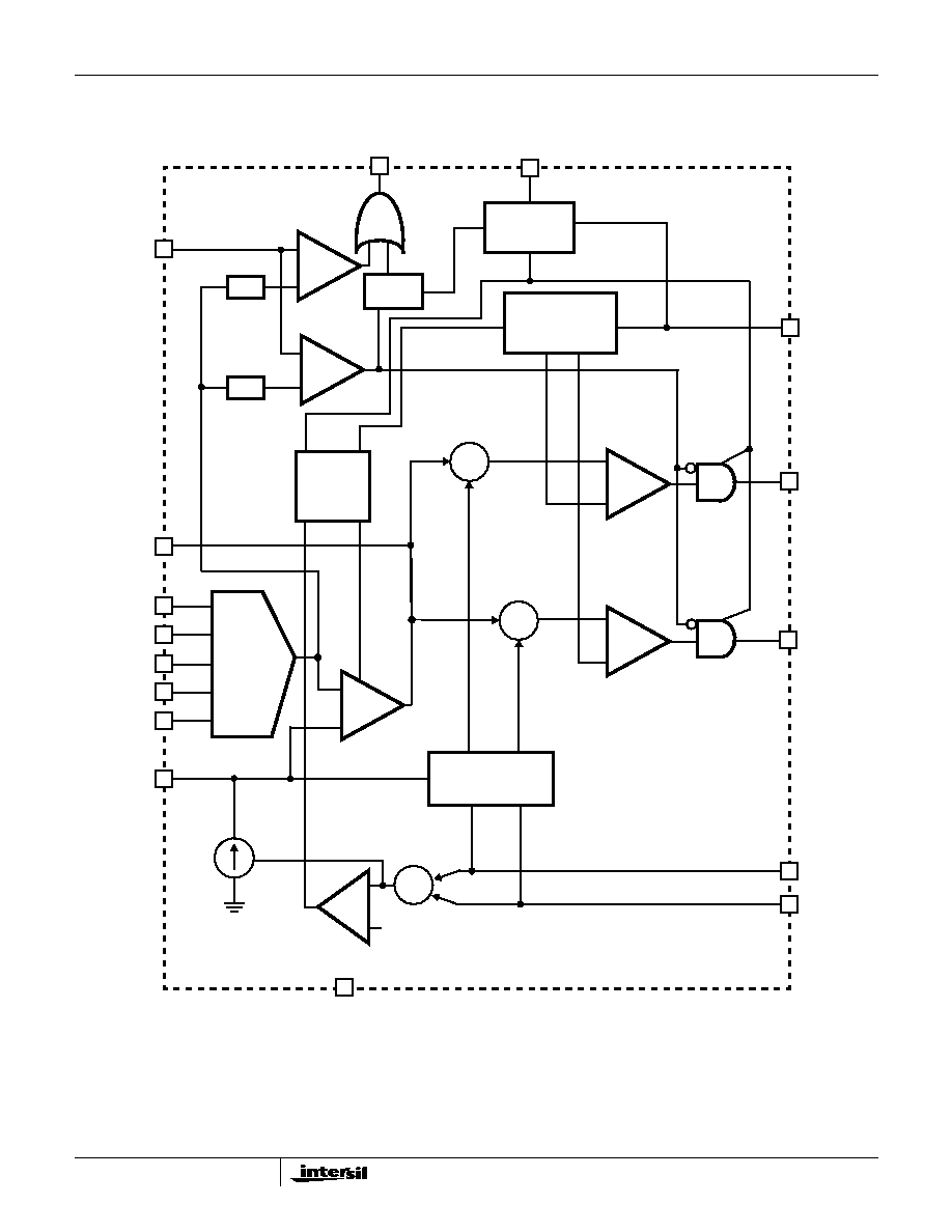
Pinout
HIP6302 (SOIC)
TOP VIEW
Ordering Information
PART NUMBER
TEMP. (
o
C)
PACKAGE
PKG. NO.
HIP6302CB
0 to 70
16 Ld SOIC
M16.15
HIP6302CB-T
16 Ld SOIC Tape and Reel
HIP6302EVAL1
Evaluation Platform
VID4
VID3
VID2
VID1
VID0
FS/DIS
VSEN
PGOOD
PWM1
PWM2
V
CC
FB
ISEN1
COMP
ISEN2
GND
14
15
16
9
13
12
11
10
1
2
3
4
5
7
6
8
Data Sheet
February 2000
CAUTION: These devices are sensitive to electrostatic discharge; follow proper IC Handling Procedures.
1-888-INTERSIL or 321-724-7143
|
Copyright
©
Intersil Corporation 2000

3
Simplified Power System Diagram
Functional Pin Description
VID4 (Pin 1), VID3(Pin 2), VID2 (Pin 3), VID1(Pin 4)
and VID0 (Pin 5)
Voltage Identification inputs from microprocessor. These pins
respond to TTL and 3.3V logic signals. The HIP6302 decodes
VID bits to establish the output voltage. See Table 1.
COMP (Pin 6)
Output of the internal error amplifier. Connect this pin to the
external feedback and compensation network.
FB (Pin 7)
Inverting input of the internal error amplifier.
FS/DIS (Pin 8)
Channel frequency, F
SW
, select and disable. A resistor from
this pin to ground sets the switching frequency of the
converter. Pulling this pin to ground disables the converter
and three states the PWM outputs. See Figure 10.
GND (Pin 9)
Bias and reference ground. All signals are referenced to this
pin.
VSEN (Pin 10)
Power good monitor input. Connect to the microprocessor-
CORE voltage.
ISEN2(Pin 11) and ISEN1(Pin 14)
Current sense inputs from the individual converter channel's
phase nodes.
PWM2 (Pin 12) and PWM1(Pin 13)
PWM outputs for each driven channel in use. Connect these
pins to the PWM input of a HIP6601/2/3 driver.
PGOOD (Pin 15)
Power good. This pin provides a logic-high signal when the
microprocessor CORE voltage (VSEN pin) is within specified
limits and Soft-Start has timed out.
V
CC
(Pin 16)
Bias supply. Connect this pin to a 5V supply.
SYNCHRONOUS
HIP6302
MICROPROCESSOR
VSEN
VID
RECTIFIED BUCK
CHANNEL
SYNCHRONOUS
RECTIFIED BUCK
CHANNEL
PWM 1
PWM 2
VID4
VID3
VID2
VID1
VID0
FS/DIS
VSEN
PGOOD
PWM1
PWM2
V
CC
FB
ISEN1
COMP
ISEN2
GND
14
15
16
9
13
12
11
10
1
2
3
4
5
7
6
8
HIP6302
HIP6302