1
®
FN7288.3
CAUTION: These devices are sensitive to electrostatic discharge; follow proper IC Handling Procedures.
1-888-INTERSIL or 321-724-7143
|
Intersil (and design) is a registered trademark of Intersil Americas Inc.
Copyright © Intersil Americas Inc. 2002-2005. All Rights Reserved.
All other trademarks mentioned are the property of their respective owners.
EL7457
40MHz Non-Inverting Quad CMOS Driver
The EL7457 is a high speed, non-inverting, quad CMOS
driver. It is capable of running at clock rates up to 40MHz
and features 2A peak drive capability and a nominal on-
resistance of just 3
. The EL7457 is ideal for driving highly
capacitive loads, such as storage and vertical clocks in CCD
applications. It is also well suited to ATE pin driving, level-
shifting, and clock-driving applications.
The EL7457 is capable of running from single or dual power
supplies while using ground referenced inputs. Each output
can be switched to either the high (V
H
) or low (V
L
) supply
pins, depending on the related input pin. The inputs are
compatible with both 3V and 5V CMOS and TTL logic. The
output enable (OE) pin can be used to put the outputs into a
high-impedance state. This is especially useful in CCD
applications, where the driver should be disabled during
power down.
The EL7457 also features very fast rise and fall times which
are matched to within 1ns. The propagation delay is also
matched between rising and falling edges to within 2ns.
The EL7457 is available in 16-pin QSOP, 16-pin SO
(0.150"), and 16-pin QFN packages. All are specified for
operation over the full -40°C to +85°C temperature range.
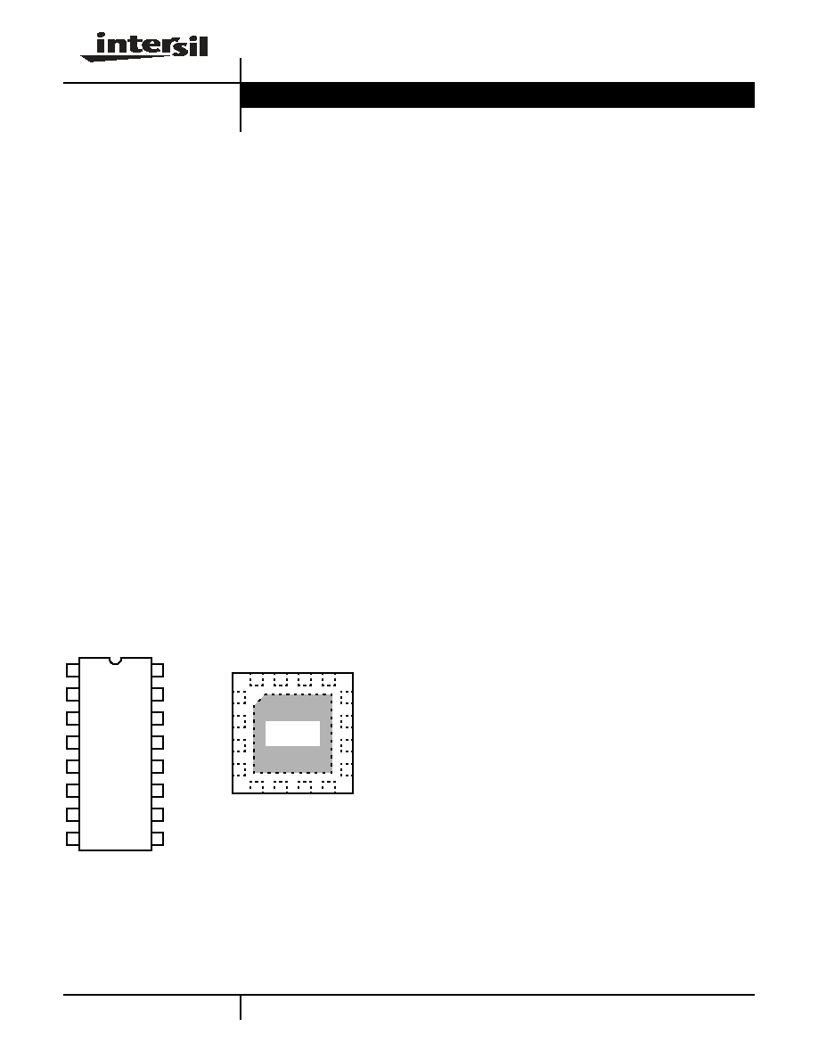
Pinouts
Features
· Clocking speeds up to 40MHz
· 4 channels
· 12ns t
R
/t
F
at 1000pF C
LOAD
· 1ns rise and fall time match
· 1.5ns prop delay match
· Low quiescent current - <1mA
· Fast output enable function - 12ns
· Wide output voltage range
· 8V
V
L
-5V
· -2V
V
H
16.5V
· 2A peak drive
· 3
on resistance
· Input level shifters
· TTL/CMOS input-compatible
· Pb-free available (RoHS compliant)
Applications
· CCD drivers
· Digital cameras
· Pin drivers
· Clock/line drivers
· Ultrasound transducer drivers
· Ultrasonic and RF generators
· Level shifting
1
2
3
4
16
15
14
13
5
6
7
12
11
10
8
9
1
2
3
4
12
11
10
9
5
6
7
8
16
15
14
13
INB
VL
VL
GND
INC
IND
VS
-
OUT
D
OE
INA
VS
+
OUT
A
OUTB
VH
VH
OUTC
THERMAL
PAD*
INA
OE
INB
VL
GND
NC
INC
IND
VS+
OUTA
OUTB
NC
VH
OUTC
OUTD
VS-
EL7457
[16-PIN SO (0.150"),
QSOP (0.150")]
TOP VIEW
EL7457
[16-PIN QFN (4x4mm)]
TOP VIEW
* THERMAL PAD CONNECTED
TO PIN 7 (V
S
-)
Data Sheet
January 3, 2005
3
FN7288.3
January 3, 2005
Absolute Maximum Ratings
(T
A
= 25°C)
Supply Voltage (V
S
+ to V
S
-) . . . . . . . . . . . . . . . . . . . . . . . . . . .+18V
Input Voltage . . . . . . . . . . . . . . . . . . . . . . . . . . V
S
- -0.3V, V
S
+ +0.3V
Continuous Output Current . . . . . . . . . . . . . . . . . . . . . . . . . . 100mA
Storage Temperature Range . . . . . . . . . . . . . . . . . .-65°C to +150°C
Ambient Operating Temperature . . . . . . . . . . . . . . . .-40°C to +85°C
Maximum Die Temperature . . . . . . . . . . . . . . . . . . . . . . . . . . +125°C
Power Dissipation . . . . . . . . . . . . . . . . . . . . . . . . . . . . . See Curves
CAUTION: Stresses above those listed in "Absolute Maximum Ratings" may cause permanent damage to the device. This is a stress only rating and operation of the
device at these or any other conditions above those indicated in the operational sections of this specification is not implied.
IMPORTANT NOTE: All parameters having Min/Max specifications are guaranteed. Typical values are for information purposes only. Unless otherwise noted, all tests
are at the specified temperature and are pulsed tests, therefore: T
J
= T
C
= T
A
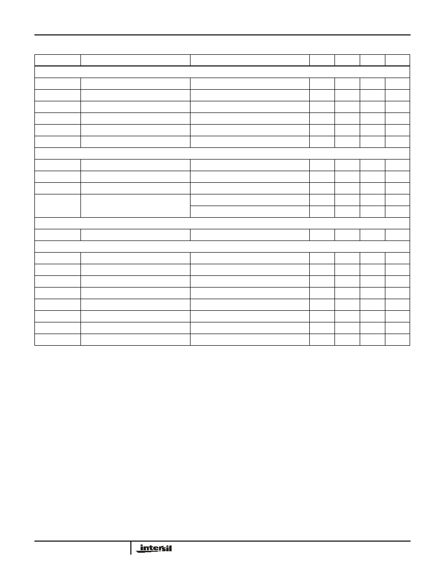
Electrical Specifications
V
S
+ = +5V, V
S
- = -5V, V
H
= +5V, V
L
= -5V, T
A
= 25°C, unless otherwise specified.
PARAMETER
DESCRIPTION
CONDITION
MIN
TYP
MAX
UNIT
INPUT
V
IH
Logic "1" Input Voltage
2.0
V
I
IH
Logic "1" Input Current
V
IH
= 5V
0.1
10
µA
V
IL
Logic "0" Input Voltage
0.8
V
I
IL
Logic "0" Input Current
V
IL
= 0V
0.1
10
µA
C
IN
Input Capacitance
3.5
pF
R
IN
Input Resistance
50
M
OUTPUT
R
OH
ON Resistance V
H
to OUTx
I
OUT
= -100mA
4.5
6
R
OL
ON Resistance V
L
to OUTx
I
OUT
= +100mA
4
6
I
LEAK
Output Leakage Current
V
H
= V
S
+, V
L
= V
S
-
0.1
10
µA
I
PK
Peak Output Current
Source
2.0
A
Sink
2.0
A
POWER SUPPLY
I
S
Power Supply Current
Inputs = V
S
+
0.5
1.5
mA
SWITCHING CHARACTERISTICS
t
R
Rise Time
C
L
= 1000pF
13.5
ns
t
F
Fall Time
C
L
= 1000pF
13
ns
t
RF
t
R
, t
F
Mismatch
C
L
= 1000pF
0.5
ns
t
D
+
Turn-Off Delay Time
C
L
= 1000pF
12.5
ns
t
D
-
Turn-On Delay Time
C
L
= 1000pF
14.5
ns
t
DD
t
D-1
- t
D-2
Mismatch
C
L
= 1000pF
2
ns
t
ENABLE
Enable Delay Time
12
ns
t
DISABLE
Disable Delay Time
12
ns
EL7457
5
FN7288.3
January 3, 2005
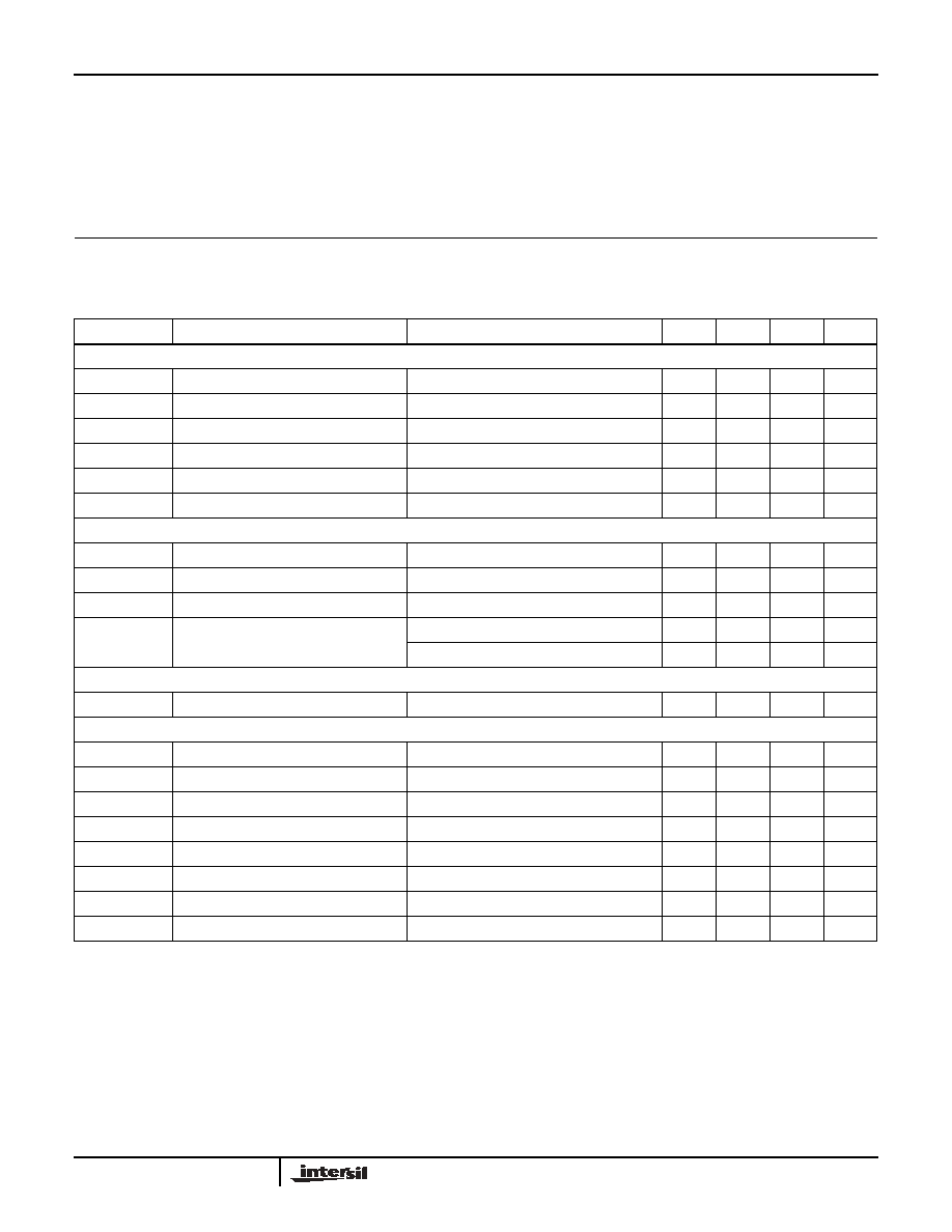
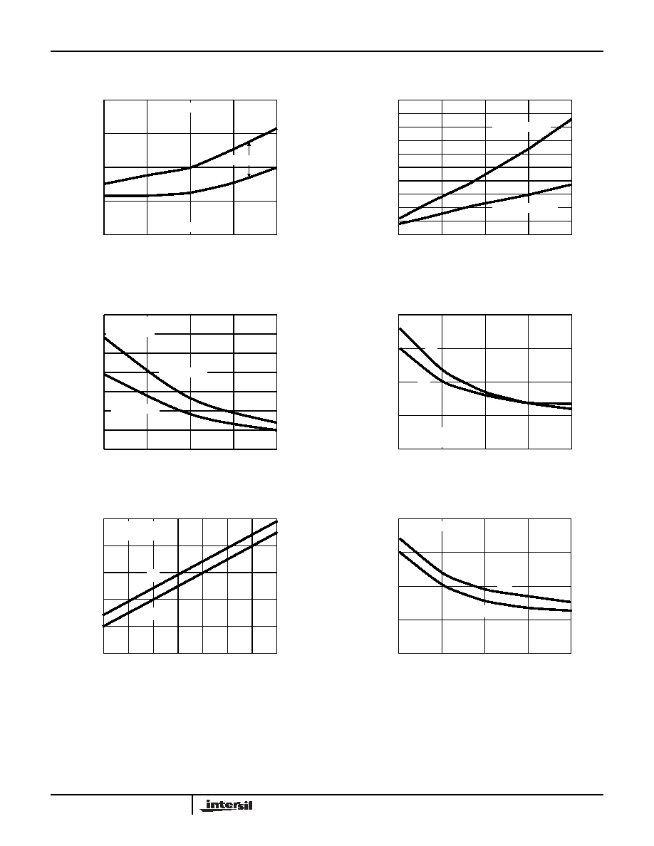
Typical Performance Curves
FIGURE 1. SWITCH THRESHOLD vs SUPPLY VOLTAGE
FIGURE 2. QUIESCENT SUPPLY CURRENT vs SUPPLY
VOLTAGE
FIGURE 3. "ON" RESISTANCE vs SUPPLY VOLTAGE
FIGURE 4. RISE/FALL TIME vs SUPPLY VOLTAGE
FIGURE 5. RISE/FALL TIME vs TEMPERATURE
FIGURE 6. PROPAGATION DELAY vs SUPPLY VOLTAGE
T=25°C
HIGH LIMIT=2.4V
LOW LIMIT=0.8V
HYSTERESIS
1.8
1.6
1.4
1.2
1
5
7
10
12
15
SUPPLY VOLTAGE (V)
I
N
PUT VO
L
T
AGE
(V)
T=25°C
ALL INPUTS=0
ALL INPUTS=V
S
+
2
1.6
1.2
0.8
0
5
7
10
12
15
SUPPLY VOLTAGE (V)
SUPP
L
Y
CURRENT
(V
)
0.4
I
OUT
=100mA
T=25°C
V
L
TO OUT
9
8
6
4
2
5
7
10
12
15
SUPPLY VOLTAGE (V)
"ON" RE
SIST
ANCE
(
)
3
7
5
V
H
TO OUT
C
L
=1000pF
T=25°C
25
20
15
10
5
5
7
10
12
15
SUPPLY VOLTAGE (V)
RI
SE
/F
ALL T
I
ME (ns)
t
F
t
R
C
L
=1000pF
V
S
+=15V
16
14
12
8
6
-50
0
50
100
125
TEMPERATURE (°C)
RIS
E
/F
ALL
TIME
(
n
s
)
t
F
t
R
10
25
75
-25
C
L
=1000pF
25
20
15
5
5
10
15
SUPPLY VOLTAGE (V)
DELA
Y TI
ME
(ns)
10
12
7
t
D2
t
D1
EL7457