 | –≠–ª–µ–∫—Ç—Ä–æ–Ω–Ω—ã–π –∫–æ–º–ø–æ–Ω–µ–Ω—Ç: LXT6234 | –°–∫–∞—á–∞—Ç—å:  PDF PDF  ZIP ZIP |

LXT6234
E-Rate Multiplexer
Datasheet
The LXT6234 E-Rate Multiplexer is a single-chip solution for multiplexing four tributary
channels into a single high speed data stream and for demultiplexing a high speed data stream
back to four tributary channels. All of the necessary circuitry is integrated into the LXT6234 E-
Rate Multiplexer; there is no need for an external framing device.
The LXT6234 E-Rate Multiplexer conforms to both the (ITU) G.742 and (ITU) G.751
multiplexing formats defined by the International Telecommunications Union (ITU; formerly
known as CCITT): G.742 recommendation for multiplexing four E1 channels into an E2 frame;
and the G.751 recommendation for multiplexing four E2 channels into an E3 frame.
The LXT6234 E-Rate Multiplexer also encodes and decodes HDB3 zero suppression line coding
used on E1, E2, and E3 signals. The coder and decoder input/output pins are externally
accessible, allowing either HDB3 or NRZ (non-return-to-zero) I/O to the multiplexer. The
LXT6234 E-Rate Multiplexer can also serve as a five channel HDB3 coder and decoder.
Applications
Product Features
n
E1/E2 Multiplexer (2/8 Mbit/s)
n
E2/E3 Multiplexer (8/34 Mbit/s)
n
E1/E3 Multiplexer (2/34 Mbit/s)
n
Digital Loop Carrier (DLC) Terminal
n
Add / Drop Multiplexers (ADM)
n
4 - to - 1 Non-Standard Multiplexer
n
Performs four-E1 to one-E2, or four-E2 to
one-E3 multiplexing. Five ICs will
implement a sixteen-E1 to one-E3
multiplexer.
n
Fully compliant with the G.742 and G.751
ITU recommendations. Fully compliant
with G.703 when used with LXT305/332
Line Interface.
n
A robust frame-acquisition and frame-
holding algorithm minimizes frame
slippage, acquires and holds frame below
10
-2
bit error rate.
n
Four auxiliary low speed data or flag
channels are available via the Stuffing Bits
on each tributary channel.
n
Access to the Alarm bit and the National
bit. These can be used as recommended by
ITU or for proprietary use.
n
Five independent HDB3 CODECs allow
multiplexer I/O in either HDB3 or NRZ
formats. The LXT6234 can also function as
a stand alone five-channel HDB3
transcoder.
As of January 15, 2001, this document replaces the Level One document
Order Number: 249301-001
LXT6234 E-Rate Multiplexer Datasheet.
January 2001

Datasheet
Information in this document is provided in connection with Intel
Æ
products. No license, express or implied, by estoppel or otherwise, to any intellectual
property rights is granted by this document. Except as provided in Intel's Terms and Conditions of Sale for such products, Intel assumes no liability
whatsoever, and Intel disclaims any express or implied warranty, relating to sale and/or use of Intel products including liability or warranties relating to
fitness for a particular purpose, merchantability, or infringement of any patent, copyright or other intellectual property right. Intel products are not
intended for use in medical, life saving, or life sustaining applications.
Intel may make changes to specifications and product descriptions at any time, without notice.
Designers must not rely on the absence or characteristics of any features or instructions marked "reserved" or "undefined." Intel reserves these for
future definition and shall have no responsibility whatsoever for conflicts or incompatibilities arising from future changes to them.
The LXT6234 may contain design defects or errors known as errata which may cause the product to deviate from published specifications. Current
characterized errata are available on request.
Contact your local Intel sales office or your distributor to obtain the latest specifications and before placing your product order.
Copies of documents which have an ordering number and are referenced in this document, or other Intel literature may be obtained by calling
1-800-548-4725 or by visiting Intel's website at http://www.intel.com.
Copyright © Intel Corporation, 2001
*Third-party brands and names are the property of their respective owners.

Datasheet
3
E-Rate Multiplexer -- LXT6234
Contents
1.0
Block Diagram
............................................................................................................. 5
2.0
Conscription
................................................................................................................. 6
3.0
Functional Description
........................................................................................... 11
3.1
Frame Format......................................................................................................11
3.2
HDB3 Codecs......................................................................................................11
3.3
HDB3 Decoder Alarms ........................................................................................ 12
3.4
Multiplexer ........................................................................................................... 12
3.4.1
Flag Bits ................................................................................................. 13
3.4.2
Multiplexer Alarms ..................................................................................14
3.5
Demultiplexer ......................................................................................................14
3.5.1
Demultiplexer Alarms ............................................................................. 14
4.0
Glossary
....................................................................................................................... 16
5.0
Application Information
.........................................................................................17
5.1
E1/E3 Multiplexer Block Diagram........................................................................ 17
5.1.1
E1 Line Interface .................................................................................... 17
5.1.2
LXT6234, E1/E2 Stage........................................................................... 17
5.1.3
LXT6234, E3 Stage ................................................................................ 18
6.0
Test Specifications
.................................................................................................. 19
7.0
AC Timing Specifications
..................................................................................... 20
Figures
1
Block Diagram ....................................................................................................... 5
2
LXT6234 Pin Assignment...................................................................................... 6
3
Multiplexer Side Block Diagram .......................................................................... 12
4
E2 Frame............................................................................................................. 13
5
E3 Frame............................................................................................................. 13
6
Demultiplexer Side Block Diagram...................................................................... 15
7
E1/E3 Multiplexer Block Diagram........................................................................ 17
8
HDB3 Encoder and Decoder Timing (Refer to
Table 5
) ...................................... 20
9
Multiplexer Tributary Input Timing (Refer to
Table 6
) .......................................... 20
10
High Speed Multiplexer Input & Output Timing (Refer to
Table 7
) ...................... 21
11
High Speed Demultiplexer Input & Output Timing (Refer to
Table 8
)..................22
12
Chip Enable Timing (Refer to
Table 9
) ................................................................ 22
13
Package Specifications ....................................................................................... 23

LXT6234 -- E-Rate Multiplexer
4
Datasheet
Tables
1
Input Signals ......................................................................................................... 7
2
Output Signals....................................................................................................... 9
3
Absolute Ratings ................................................................................................. 19
4
DC Characteristics (TA=-40 to +85◊C, Vdd=+5V±5%, GND=0 V)...................... 19
5
HDB3 Encoder and Decoder (Refer to
Figure 8
) ............................................... 20
6
Multiplexer Tributary Input (Refer to
Figure 9
) ................................................... 21
7
High Speed Multiplexer Input & Output (Refer to
Figure 10
) ............................. 21
8
High Speed Demultiplexer Input & Output (Refer to
Figure 11
) ......................... 22
9
Chip Enable (Refer to
Figure 12
) ........................................................................ 22
10
100-Pin Plastic Quad Flat Packs......................................................................... 23
E-Rate Multiplexer -- LXT6234
Datasheet
5
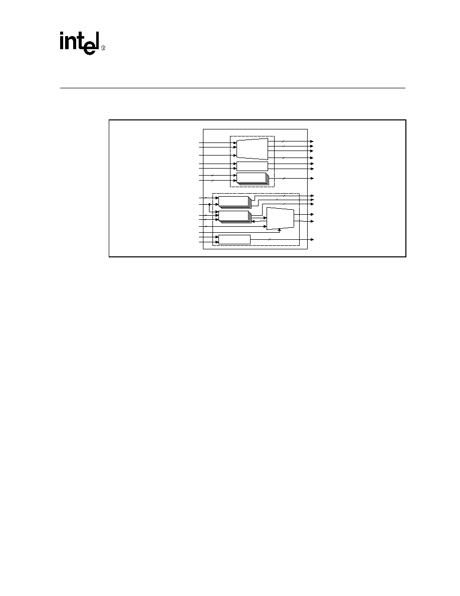
1.0
Block Diagram
Figure 1. Block Diagram
Multiplexer
HDB3
Decoder #[1:4]
Elastic Store
Multiplexer
And
Timing
Control
HDB3 Encoder
4 Tributary NRZ Data Outputs
4 Clocks
Service Channels / AIS
Demultiplexer
And
Timing
Control
Mode Select
Demultiplexer
HDB3 Decoder
HDB3
Encoder #[1:4]
High Speed NRZ Data Input
Clock
HDB3 Data Input
Clock
4 Tributary NRZ Data Inputs
4 Clocks
4
4
4
4
NRZ Data Output
Bipolar Violation Alarm
6
4 HDB3 Pos/Neg Data Output P
4 HDB3 Pos/Neg Data Input Pairs
4 Clocks
8
4 Force AIS
4 NRZ Data Inputs
Service Channels / Ref Clock
High Speed Multiplexer Clock
NRZ Data Input
Clock
4
4
4
4
4 NRZ Data Outputs
4 Elastic Store Alarm Indication
4 Bipolar Violation Alarms
4
4
4
8
High Speed NRZ Data Output
Frame Sync Pulse
Pos/Neg Data Output Pair
2
Loss Of Signal (LOS)