Product Description
In today's price-sensitive communications
environment, network equipment designers are
seeking flexible, high-performance integrated
circuitries for cost-effective timing applications
in a wide variety of optical-network designs.
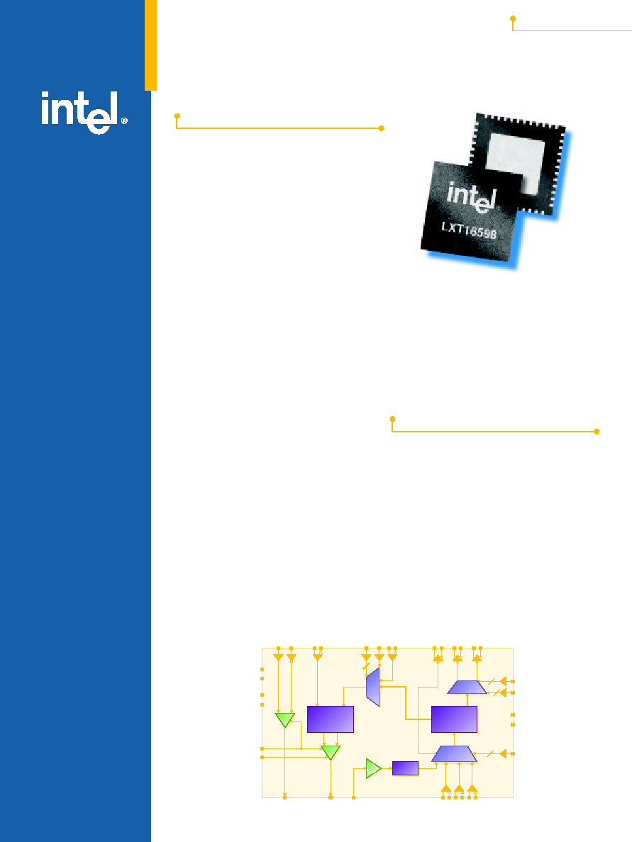
The Intel
Æ
LXT16598L/H is a generic Phase
Locked Loop (PLL) clock synthesizer in two
versions to support different frequency ranges:
∑
The Intel LXT16598L on-board Voltage
Controlled Oscillator (VCO) supports the
frequency range of 622MHz to 675MHz.
∑
The Intel LXT16598H on-board VCO
supports the frequency range of 675MHz
to 809MHz.
The LXT16598L/H is used in SDH STM 16/64
and SONET OC-48/192 telecommunications
systems, Optical Transport Network (OTN)
systems with Forward Error Correction (FEC),
Gigabit Ethernet systems, and fiber-optic test
equipment. The device features a Phase
Frequency Comparator (PFC), LC-VCO, and
has three separate, programmable differential
clock outputs in the range between 1/1 and
1/64 of the reference clock.
The system reference clock may range from
9MHz to 809MHz, and can select up to three
external VCXO/VCSOs in addition to the
on-board VCO. The polarity of VCXO/VCSO
driver outputs can be changed to support
VCXO/VCSOs, with either positive or negative
gain constants.
This two-chip solution can be used to support
up to 30 percent overhead for 10Gbps FEC
applications. The devices are housed in a
Intel
Æ
LXT16598L and LXT16598H
622MHz/809MHz Generic Phase Locked Loop (PLL) Clock Synthesizers
product brief
48-pin QFN 7x7mm low form factor package,
and are operated from a single +3.3V power
supply with a low power dissipation, less than
0.5W.
With the Intel LXT16598L/H, customers can
focus resources on features that differentiate
their products from the competition instead of
having to design their own clock architectures
or use more costly modules.
Key Applications
∑
SDH STM 16/64, SONET OC-48/192 FEC
or OTN applications--can be used as a
gearbox for synchronous or asynchronous
clocking operation with FEC devices from
Intel or third parties
∑
SDH STM 64, SONET OC-192 Metro/
Long-Haul Modules--can be used for clock
synthesis in MSA modules
∑
SDH STM 16/64, SONET OC-48/192,
or GbE applications--can be used for jitter
cleanup, where the incoming system
reference clock is cleaned against an
external VCXO
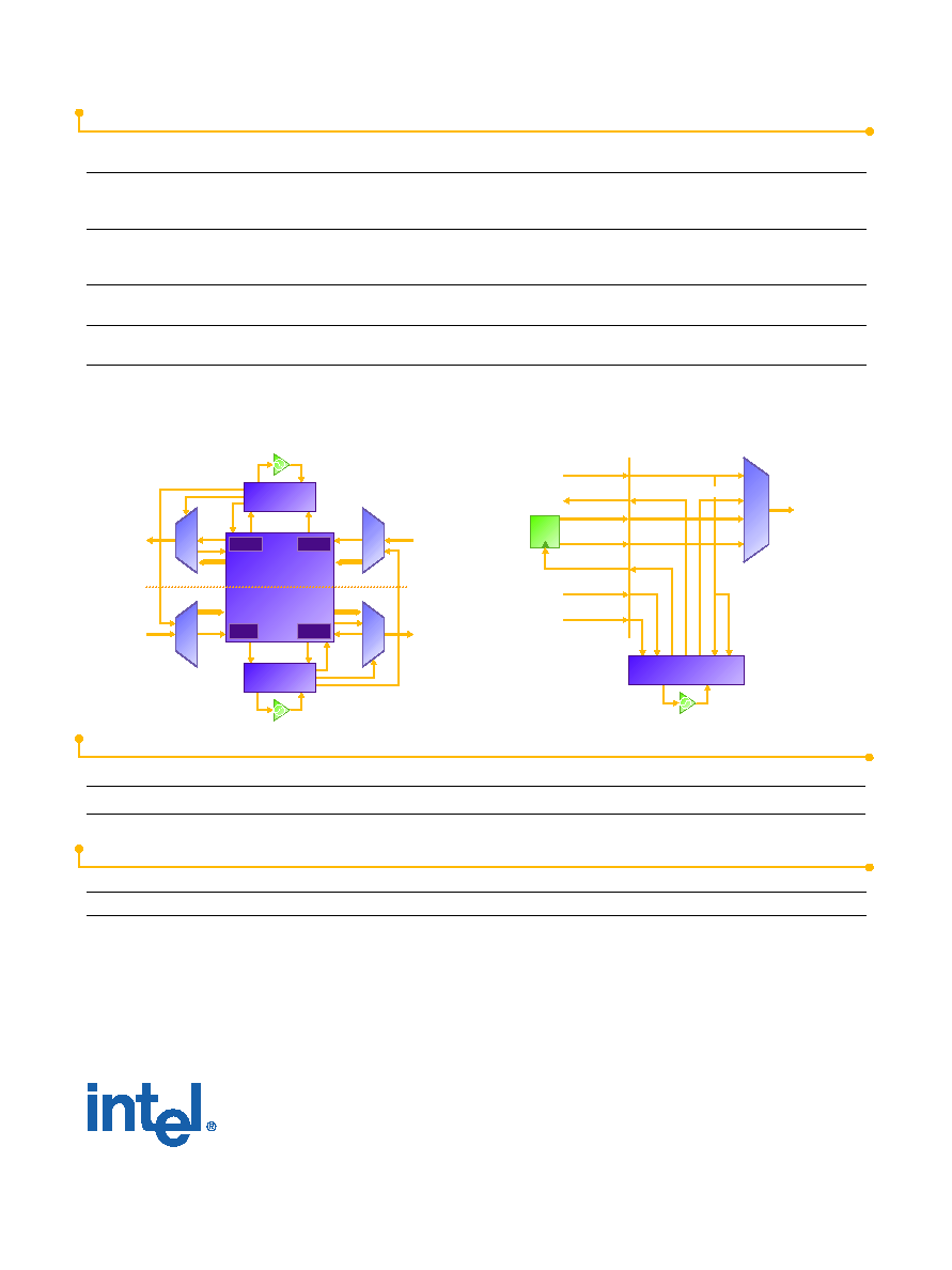
OUCHP2
FOUTBN
FOUTB
FOUTCN
FOUTC
FOUT
AN
FOUT
A
FIN
FI
FISEL
CSEL0...1
BSEL0...2
DIVSEL0...2
DOWN
UP
COFSCHP1
VCCA
VCC
VEEA
VEE
SGNX
CKREFN
CKREF
VCXO3N
VCXO3
VCXO2N
VCXO2
VCXO1N
VCXO1
3
2
DIODEE
DIODEC
VCOSEL0...1
OUCHP1
VCTL
2
3
Divide by
1, 2, 4, 8,
16, 32, 64
Selector
Selector
CHAP
CHAP
PFD
FV
FR
Divider
Block Diagram
Selector
4:1
UNITED STATES AND CANADA
Intel Corporation
Robert Noyce Bldg.
2200 Mission College Blvd.
P.O. Box 58119
Santa Clara, CA 95052-8119
USA
EUROPE
Intel Corporation (UK) Ltd.
Pipers Way
Swindon
Wiltshire SN3 1RJ
UK
ASIA-PACIFIC
Intel Semiconductor Ltd.
32/F Two Pacific Place
88 Queensway, Central
Hong Kong
JAPAN
Intel Japan (Tsukuba HQ)
5-6
Tokodai Tsukuba-shi
300-2635 Ibaraki-ken
Japan
SOUTH AMERICA
Intel Semicondutores do Brasil Ltda
Av. Dr. Chucri Zaidan, 940-10∞ andar
04583-904 S„o Paulo, SP
Brazil
© 2002 Intel Corporation
Order Number: 251139-001 0602/MG/DC/DC/MG/1K
Information in this document is provided in connection with Intel
Æ
products. No license, express or implied, by estoppel or otherwise,
to any intellectual property rights is granted by this document. Except as provided in Intel's Terms and Conditions of Sale for such
products, Intel assumes no liability whatsoever, and Intel disclaims any express or implied warranty, relating to sale and/or use of Intel
products including liability or warranties relating to fitness for a particular purpose, merchantability, or infringement of any patent,
copyright, or other intellectual property right. Intel products are not intended for use in medical, life-saving or life-sustaining applications.
Intel may make changes to specifications and product descriptions at any time, without notice.
Designers must not rely on the absence or characteristics of any features or instructions marked "reserved" or "undefined." Intel
reserves these for future definition and shall have no responsibility whatsoever for conflicts or incompatibilities arising from future
changes to them.
Intel and the Intel Logo are trademarks or registered trademarks of Intel Corporation or its subsidiaries in the United States or other
countries.
* Other names and brands may be claimed as the property of others.
Intel Access
Developer's Site
http://developer.intel.com
Networking Components Home Page
http://developer.intel.com/design/network
Other Intel Support:
http://developer.intel.com/design/litcentr
Intel Literature Center
(800) 548-4725 7 a.m. to 7 p.m. CST (U.S. and Canada)
International locations please contact your local sales office.
General Information Hotline
(800) 628-8686 or (916) 356-3104 5 a.m. to 5 p.m. PST
Features Benefits
s
On-board VCO with support for up to 809MHz
s
Single chip solution helps reduce board space
for applications demanding a high Q
s
Support for three optional VCXO/VCSOs in a single
s
Provides seamless gear-box implementation with Intel
Æ
FEC
chip solution
devices and ensures seamless support for multiple line
speeds without using external components
s
Programmable output rates and scalable output bit rates
s
Delivers flexibility and reusability across multiple designs
with these division ratios of input: /1, /2, /4, /8, /16, /32,
while reducing design and production costs
and /64
s
Supports ITU-T G.709 and G.975 to be used in FEC
s
Single chip solution offers a high coding gain for advanced
and Digital Wrapping applications
OTN system solutions
s
48-pin QFN (7x7mm) package
s
Small physical form factor simplifies design and helps reduce
board space
s
Silicon bipolar process technology
s
Delivers well-proven, high-performance technology and
reliable, high-volume manufacturing
FEC/OTN
Device
LXT16707
MUX
LXT16706
DeMUX
LXT16598
Gear-Box Application
:n
:m
:n
:m
Up to 3 VCXOs
Up to 3 VCXOs
LXT16707
MUX
LXT16706
DeMUX
OC-192
9.95Gbps
10.7Gbps
16 x 622MHz
16 x 669MHz
3 clock outputs 669MHz
3 clock outputs 622MHz
LXT16598
Clock Synthesis
VCXO
(optional)
MSA300 Interface
TxREFSEL
155/622MHz
TxREFSEL
155/622MHz
TxMCLK_P/N
311/622MHz
TxREFCLK_P/N
311/622MHz
TxPICLK_P/N
311/622MHz
TxDIN
TxPCLK_P/N
622MHz
Intel
Æ
or 3r
d Party
MUX
LXT16598
OC-192
9.95Gbps
CSEL0...1
BSEL0...1
FOUTC
FOUTB
FOUT
A
DIVSEL
CKREF
TXREFCLK
Support Collateral
Item
Description
Order Number
LXT16598
Datasheet for LXT16598L/H
251064
LXD90598
Evaluation Board Datasheet
251065