 | ÐлекÑÑоннÑй компоненÑ: LXT16596 | СкаÑаÑÑ:  PDF PDF  ZIP ZIP |
PB LXT16596-97

Intel
®
Internet Exchange
Architecture
Product Description
The Intel
®
LXT16596 and Intel
®
LXT16597
form a high-performance transponder
chipset for use in SDH STM-16/4/1, SONET
OC-48/12/3 telecommunications systems,
and Optical Transport Network (OTN) sys-
tems with digital wrapping.
The LXT16596 receiver is an on-the-fly
programmable multi-bitrate Clock and Data
Recovery (CDR) device with a 1:4
Demultiplexer (DeMUX), integrated Clock
Multiplication Unit (CMU), and a Limiting
Amplifier (LIA).
The LXT16597 transmitter is an on-the-fly
programmable multi-bitrate 4:1 multiplexer
(MUX) with integrated clock generation and
Phase Locked Loop (PLL) circuits. The inte-
grated chipset ensures simple board design.
The fully integrated on-chip PLLs elimi-
nate critical clock and data timing relations
product brief
and feature the unique dynamic phase align-
ment between ASIC and MUX. The continu-
ous handling of "round trip delay variations"
by the source synchronous clocking ensures
easy external optimization of jitter.
The Intel
®
LXT16596/97 chipset is manu-
factured in a well-proven silicon bipolar tech-
no-logy that offers the performance, stability
and reliability customers require for optical
communication systems.
The devices are operated from a single
+3.3V power supply with a power dissipation
of 1.0W for LXT16597 and 1.25W for
LXT16596.
I
Single Power Supply: +3.3V
I
Easy board design and integration
I
Power dissipation: 1.25W
I
High integration
I
Interfaces to Intel
®
IXF32003 and
I
Advanced system solution integrating odd
Intel
®
IXF6192
ratio digital wrapping
I
OIF compliant interface
I
Complete CDR secures interoperability
between Demultiplexer and Framer
I
100-lead plastic package
I
Small physical form factor (14x14mm).
Reduces board space
I
Integrated limiting amplifier
I
Avoid external limiting amplifier. Cost and
space savings
LXT16596 Receiver
Features
Benefits
I
Single Power Supply: +3.3V
I
Easy board design and integration
I
Power dissipation: 1.0W
I
High integration
I
Interfaces to Intel
®
IXF32003 and
I
Advanced system solution integrating odd
Intel
®
IXF6192
ratio digital wrapping
I
Dynamic Phase Alignment based on PLL
I
Infinite phase margin tolerance
I
100-lead plastic package
I
Small physical form factor (14x14mm).
Reduces board space
LXT16597 Transmitter
Features
Benefits
Intel
®
LXT16596/LXT16597
Transmitter/Receiver Chipset

Key Features
I
The Intel
®
LXT16596/97 multi-bitrate chipset is distin-
guished by a low power dissipation and is compatible
with the following line rates:
I
2.488Gbit/s
I
1.250Gbit/s
I
622.08Mbit/s
I
155.52Mbit/s
I
It offers the possibility of transmitting and receiving
data at increased rates if overhead is needed.
Fractions available are 32/31, 16/15 and 15/14, which
is needed for Forward Error Correction (FEC) applica-
tions.
I
The LXT16596 receiver features an integrated limiting
amplifier with an input sensitivity better than 10mV.
Key Applications
I
SDH STM-16/4/1
I
SONET OC-48/12/3
I
OTN
Application Overview
The Intel family of receiver and transmitter line cards are
high performance MUX and DeMUX functions in a variety
of system configurations.
Receiver line card
An optical reception system receives an optical signal
and converts it into an electrical signal. The optical
receiver, which can be a PIN diode or an Avalanche
Photo Detector (APD), converts the optical input to a
small electrical current. A Transimpedance Amplifier (TIA)
also known as a pre-amplifier, then converts the current
to an electrical voltage. The TIA signal, which varies from
a few mV up to 50mVpp or more, can be passed to an
Automatic Gain Controlled (AGC) amplifier or a LIA. This
produces a signal of sufficient amplitude/power to drive
the next building block (See figure 1). A CDR device con-
verts the analog input signal to a digital bit stream with an
associated clock, and the serial high-speed data stream
is finally converted to a parallel signal at lower speed.
This signal then interfaces to the digital processing sys-
tem.
The key function block in the CDR is the PLL, which
locks onto the incoming data stream. The phase detector
is equipped with a discriminator that evaluates the
incoming data signal in the middle of the bit period (the
"eye") and determines whether a 1 or a 0 is received.
A separate lock detector determines whether the
incoming data rate deviates too much from a given fre-
quency. If data input is absent or deviates too much, the
external reference clock ensures that the Voltage
Controlled Oscillator (VCO) remains in a selectable +/-500
to +/-2,000 ppm capture range.
Phase noise and amplitude noise, also known as jitter,
can cause incorrect determination of data bits (bit errors)
in the input signal. When a valid input signal is applied
both differential data and clock outputs are provided.
The DeMUX transforms the serial data signal into four
parallel data signals at a corresponding lower data rate.
If, for example, a 2.488Gbit/s signal (OC-48/STM-16) is
fed into a 1:4 DeMUX, it will produce four parallel data
outputs at 622.08Mbit/s.
Clock output from the CDR is used to clock the data
on the parallel interface into the next device. The Intel
®
LXT16596 has a DeMUX merged with a CDR and is fully
compliant with the Optical Interface Forum's SFI recom-
mendation on common electrical interface between framers
and Serializer/Deserializer (SerDes) for OC-48/STM-16.
Transmitter line card
In the optical transmission system the parallel signal from
the processing system is converted to a serial signal at
the bitrate of the optical link. The serial signal is amplified
before it is fed to the laser, which converts it to an optical
SIC
O/E
TIA
LIA /AGC
DeMUX
Figure 1. Typical receiver line card
signal. The quality of the transmitted optical signal
(i.e., the maximum transmission distance) is highly
dependent on the jitter of the serial bit stream. The jitter is
the phase noise most commonly caused by the uncer-
tainty or variations in the bit periods. To resolve this, Intel
has directed significant effort towards the system and
component design, focused at maintaining precise, con-
stant duration of the bit periods in the outgoing data
stream (see figure 2).
The MUX has the opposite functions of the DeMUX.
For instance, the MUX might convert a 4-bit parallel sig-
nal into one serial bit stream at a corresponding higher
data rate. When four parallel inputs at 622.08Mbit/s are
fed into a 4:1 MUX, the output data rate will be
2.488Gbit/s for OC-48/STM-16.
The clock interconnections between the MUX and the
data source (such as the framer) can be complex in high-
speed applications. In high-speed clock operation for
MUXs, the input sampling clock must be in the phase to
ensure correct loading of the data into the MUXs so that
input data can be sampled correctly. In addition, the
internal high-speed clock used for shifting data to the
laser must be as clean as possible to minimize the jitter in
the output signal. Three PLLs are implemented in each
MUX to accommodate these critical requirements.
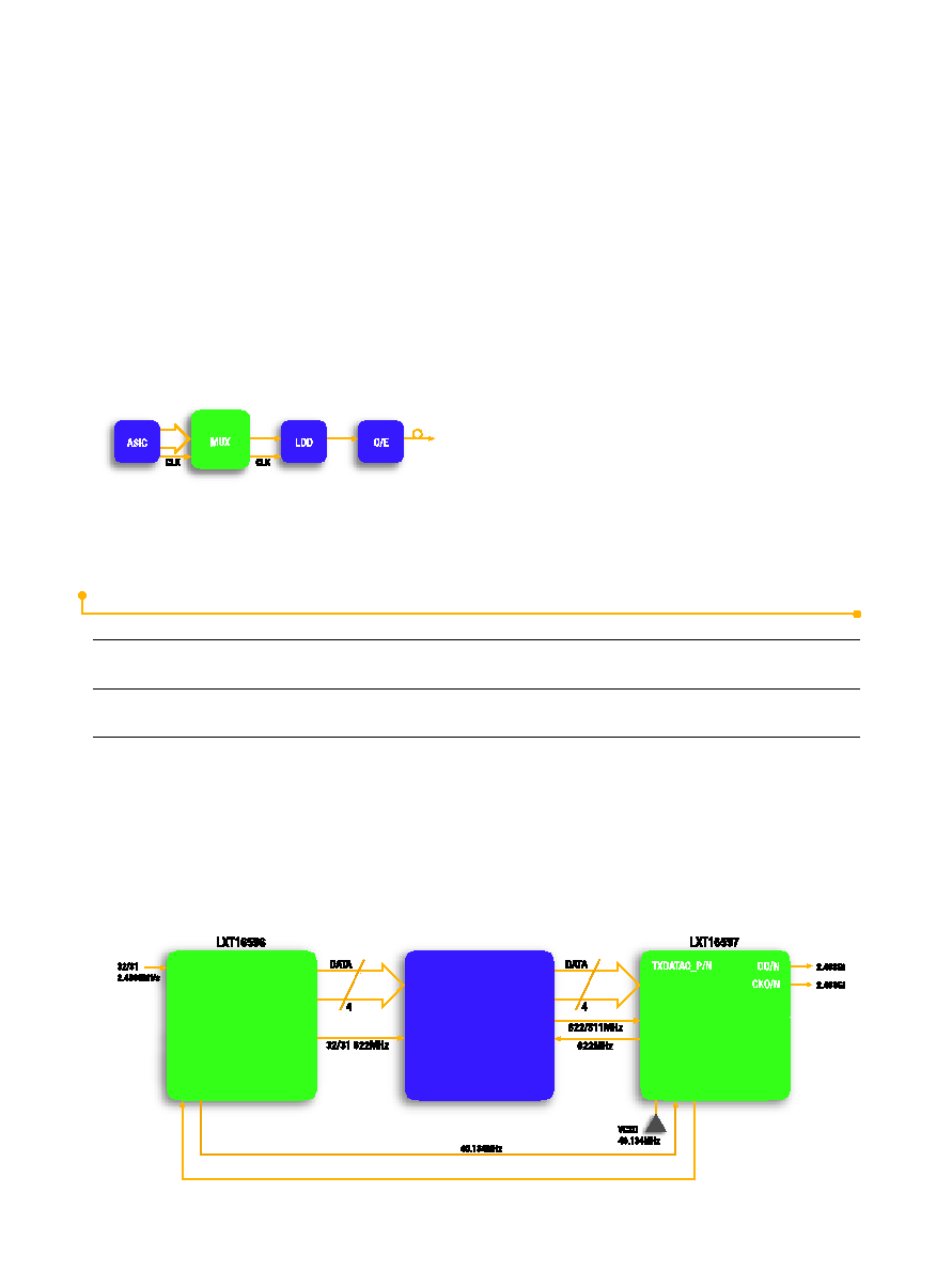
System
ASIC
RXCKL_P/N
RXDATA3_P/N
RXDATA0_P/N
.....
C
KREF
/N
F
C
K
/N
DI/N
Hz
40.134MHz
TXCLK_P/N
TXDATA3_P/N
.....
bit/s
X
C
K1
/N
C
KI
/N
RE
CC
K
/N
TXCLK_SRC_P/N
Figure 2. Typical transmitter line card
Figure 3. System Application Layout
Support Collateral/Tools
Item
Description
Order Number
Data Sheets
I
LXT16596/97 Data sheet
249700
I
LXD90596/97 Evaluation board data sheet
249701
Support Products
I
LXD90596/97 Evaluation board and gerber files
Contact local sales rep
I
LXT16596/97 Footprint
Contact local sales rep
Application Brief
I
Building Blocks for SONET/SDH Network Elements
249508
and Aggregation
Intel Access
Developer's Site
http://developer.intel.com
Intel
®
Internet Exchange Architecture Home Page
http://www.intel.com/IXA
Networking Components Home Page
http://developer.intel.com/design/network
Other Intel Support:
http://developer.intel.com/design/litcentr
Intel Literature Center
(800) 548-4725 7 a.m. to 7 p.m. CST (U.S. and Canada)
International locations please contact your local sales office.
General Information Hotline
(800) 628-8686 or (916) 356-3104 5 a.m. to 5 p.m. PST
UNITED STATES AND CANADA
Intel Corporation
Robert Noyce Bldg.
2200 Mission College Blvd.
P.O. Box 58119
Santa Clara, CA 95052-8119
USA
EUROPE
Intel Corporation (UK) Ltd.
Pipers Way
Swindon
Wiltshire SN3 1RJ
UK
ASIA-PACIFIC
Intel Semiconductor Ltd.
32/F Two Pacific Place
88 Queensway, Central
Hong Kong
JAPAN
Intel Japan (Tsukuba HQ)
5-6
Tokodai Tsukuba-shi
300-2635 Ibaraki-ken
Japan
SOUTH AMERICA
Intel Semicondutores do Brasil Ltda
Av. Dr. Chucri Zaidan, 940-10° andar
04583-904 São Paulo, SP
Brazil
Intel is a trademark or registered trademark of Intel Corporation or its subsidiaries in the United States and other countries.
Information in this document is provided in connection with Intel products. No license, express or implied, by estoppel or otherwise,
to any intellectual property rights is granted by this document. Except as provided in Intel's Terms and Conditions of sale for such
products, Intel assumes no liability whatsoever, and Intel disclaims any express or implied warranty relating to sale and/or use of Intel
products, including liability or warranties relating to fitness for a particular purpose, merchantability, or infringement of any patent,
copyright, or other intellectual property right. Intel products are not intended for use in medical, life-saving, or life-sustaining applications.
Intel may make changes to specifications and product descriptions at any time, without notice.
Designers must not rely on the absence or characteristics of any features or instructions marked "reserved" or "undefined."
Intel reserves these for future definition and shall have no responsibility whatsoever for conflicts or incompatibilities arising from future
changes to them.
* Other names and brands may be claimed as the property of others.
© 2001 Intel Corporation
Order Number: 249654-001 Printed in US/0601/5K/LOFI/LKL
Intel
®
Internet Exchange Architecture
Intel
®
Internet Exchange Architecture is an end-to-end
family of high-performance, flexible and scalable hardware
and software development building blocks designed to
meet the growing performance requirements of today's
networks. Based on programmable silicon and software
building blocks, Intel
®
IXA solutions enable faster devel-
opment, more cost-effective deployment and future
upgradability of network and communications systems.
Additional information can be found at www.intel.com/IXA
Physical Layer Devices