 | –≠–ª–µ–∫—Ç—Ä–æ–Ω–Ω—ã–π –∫–æ–º–ø–æ–Ω–µ–Ω—Ç: IMP5218 | –°–∫–∞—á–∞—Ç—å:  PDF PDF  ZIP ZIP |

Key Features
x
SCSI plug and play
-- Dual disconnect pins
-- Logic LOW disconnects lines
x
Hot swap compatible
x
Ultra-Fast response for Fast-20 SCSI applications
x
35MHz channel bandwidth
x
3.5V operation
x
Less than 3pF output capacitance
x
375µA disable-mode current
x
Thermally self limiting
x
No external compensation capacitors
x
Implements 8-bit or 16-bit (wide) applications
x
Compatible with active negation drivers
(60mA/channel)
x
Compatible with passive and active terminations
x
Approved for use with SCSI 1, 2, 3 and UltraSCSI
Block Diagrams
DISCONNECT 1
DISCONNECT 2
Current
Biasing
Circuit
Thermal
Limiting
Circuit
24mA Current
Limiting Circuit
Term Power
DATA OUTPUT
PIN DB (0)
1 of 9 Channels
2.85V
5218_01.eps
9-Line Plug and Pla
9-Line Plug and Pla
y
y
SCSI T
SCSI T
er
er
minat
minat
or
or
The 9-channel IMP5218 SCSI terminator is part of IMP's family of high-
performance SCSI terminators that deliver true UltraSCSI performance.
The BiCMOS design offers superior performance over first generation
linear regulator/resistor based terminators.
The IMP5218 has two disconnect pins for SCSI Plug and Play (PnP)
applications.
IMP's new architecture employs high-speed adaptive elements for each
channel, thereby providing the fastest response possible - typically
35MHz, which is 100 times faster than the older linear regulator termi-
nator approach. The bandwidth of terminators based on the older
regulator/resistor terminator architecture is limited to 500kHz since a
large output stabilization capacitor is required. The IMP architecture
eliminates the external output compensation capacitor and the need
for transient output capacitors while maintaining pin compatibility
with first generation designs. Reduced component count is inherent
with the IMP5218.
The IMP5218 architecture tolerates marginal system designs. A key
improvement offered by the IMP5218 lies in its ability to insure reliable,
error-free communications even in systems which do not adhere to rec-
ommended SCSI hardware design guidelines, such as improper cable
lengths and impedance. Frequently, this situation is not controlled by the
peripheral or host designer.
For portable and configurable peripherals, the IMP5218 can be placed in
a sleep mode with two disconnect signals. When disabled, the quiescent
current is typically 375
µ
A, and the outputs are in a high impedance state.
IMP5
IMP5
1
1
1
1
1/5
1/5
1
1
1
1
2
2
IMP52
IMP52
1
1
8
8
© 2000 IMP, Inc.
Data Communications 1
D
ATA
C
OMMUNICATIONS
2
408-432-9100/www.impweb.com
© 2000 IMP, Inc.
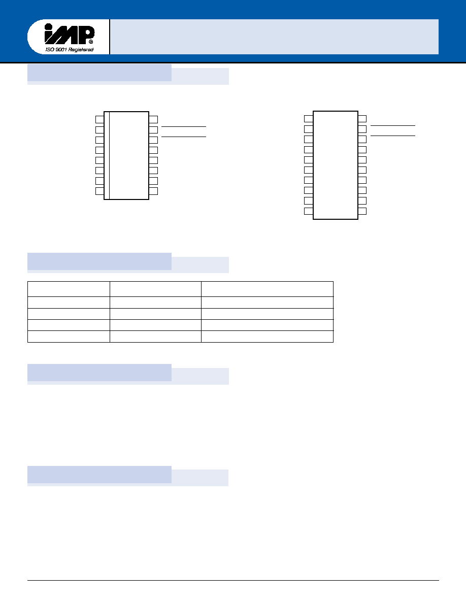
Pin Configuration
Ordering Information
Absolute Maximum Ratings
1
8
GND
1
TERM POWER
DW Package
9
GND
7
D4
10 D5
6
D3
11 D6
5
D2
12 D7
4
D1
13 D8
3
D0
14 DISCONNECT 2
2
NC
15 DISCONNECT 1
16 TERM POWER
5218_02.eps
IMP5218
SOWB-16
10
GND
1
TERM POWER
PW Package
11 GND
7
D3
14 D6
8
D4
13 D5
9
NC
12 NC
6
D2
15 NC
5
D1
16 D7
4
D0
17 D8
3
NC
18 DISCONNECT 2
2
NC
19 DISCONNECT 1
20 TERM POWER
5218_02a.eps
IMP5218
TSSOP-20
r
e
b
m
u
N
t
r
a
P
e
g
n
a
R
e
r
u
t
a
r
e
p
m
e
T
e
g
a
k
c
a
P
W
D
C
8
1
2
5
P
M
I
0∞
5
2
1
o
t
C
∞C
B
W
O
S
c
i
t
s
a
l
P
n
i
p
-
6
1
T
W
D
C
8
1
2
5
P
M
I
0∞
5
2
1
o
t
C
∞C
B
W
O
S
c
i
t
s
a
l
P
n
i
p
-
6
1
,
l
e
e
R
d
n
a
e
p
a
T
W
P
C
8
1
2
5
P
M
I
0∞
5
2
1
o
t
C
∞C
P
O
S
S
T
c
i
t
s
a
l
P
n
i
p
-
0
2
T
W
P
C
8
1
2
5
P
M
I
0∞
5
2
1
o
t
C
∞C
P
O
S
S
T
c
i
t
s
a
l
P
n
i
p
-
0
2
,
l
e
e
R
d
n
a
e
p
a
T
3
t
a
.
1
0
t
_
8
1
2
5
Thermal Data
Continuous Termination Voltage . . . . . . . . . . . 10V
Continuous Output Voltage Range . . . . . . . . 0V to 5.5V
Continuous Disable Voltage Range . . . . . . . . 0V to 5.5V
Operating Junction Temperature . . . . . . . . . . 0
∞
C to 125
∞
C
Storage Temperature Range . . . . . . . . . . . . . . ≠65
∞
C to 150
∞
C
Lead Temperature (Soldering, 10 sec.) . . . . . . 300
∞
C
Note:
1. Exceeding these ratings could cause damage to the device. All
voltages are with respect to Ground. Currents are positive
into, negative out of the specified terminal.
DW Package:
Thermal Resistance Junction-to-Ambient,
JA
. . . . . . 95
∞
C/W
PW Package:
Thermal Resistance Junction-to-Ambient,
JA
. . . . . . 144
∞
C/W
Junction Temperature Calculation: T
J
= T
A
+ (P
D
x
JA
).
The
JA
numbers are guidelines for the thermal performance of the
device/pc-board system. All of the ambient airflow is assumed.
IMP5
IMP5
1
1
1
1
1/5
1/5
1
1
1
1
2
2
IMP52
IMP52
1
1
8
8

© 2000 IMP, Inc.
Data Communications
3
Recommended Operating Conditions
2
r
e
t
e
m
a
r
a
P
l
o
b
m
y
S
n
i
M
p
y
T
x
a
M
s
t
i
n
U
e
g
a
t
l
o
V
r
w
p
m
r
e
T
V
M
R
E
T
5
.
3
5
.
5
V
e
g
a
t
l
o
V
t
u
p
n
I
e
l
b
a
s
i
D
l
e
v
e
L
h
g
i
H
V
H
I
2
V
M
R
E
T
V
e
g
a
t
l
o
V
t
u
p
n
I
e
l
b
a
s
i
D
l
e
v
e
L
w
o
L
V
L
I
0
8
.
0
V
e
g
n
a
R
e
r
u
t
a
r
e
p
m
e
T
n
o
i
t
c
n
u
J
g
n
i
t
a
r
e
p
O
0
5
2
1
C
∞
.
l
a
n
o
i
t
c
n
u
f
s
i
e
c
i
v
e
d
e
h
t
h
c
i
h
w
r
e
v
o
e
g
n
a
r
e
h
t
e
t
a
c
i
d
n
i
s
n
o
i
t
i
d
n
o
c
g
n
i
t
a
r
e
p
o
d
e
d
n
e
m
m
o
c
e
R
.
2
:
e
t
o
N
s
p
e
.
2
0
t
_
8
1
2
5
Electrical Characteristics
Unless otherwise specified, these specifications apply at an ambient operating temperature of T
A
=
25
∞
C. TermPwr = 4.75V. Low duty cycle
pulse testing techniques are used which maintain junction and case temperatures equal to the ambient temperature.
r
e
t
e
m
a
r
a
P
l
o
b
m
y
S
s
n
o
i
t
i
d
n
o
C
n
i
M
p
y
T
x
a
M
s
t
i
n
U
e
g
a
t
l
o
V
h
g
i
H
t
u
p
t
u
O
V
T
U
O
5
6
.
2
5
8
.
2
V
t
n
e
r
r
u
C
y
l
p
p
u
S
r
w
P
m
r
e
T
I
C
C
n
e
p
O
=
s
e
n
il
a
t
a
d
ll
A
6
9
A
m
V
5
.
0
=
s
e
n
il
a
t
a
d
ll
A
5
1
2
5
2
2
A
m
V
0
=
2
,
1
s
n
i
P
T
C
E
N
N
O
C
S
I
D
5
7
3
µ
A
t
n
e
r
r
u
C
t
u
p
t
u
O
I
T
U
O
V
T
U
O
V
5
.
0
=
1
2
≠
3
2
≠
4
2
≠
A
m
t
n
e
r
r
u
C
t
u
p
n
I
e
l
b
a
s
i
D
I
N
I
V
5
7
.
4
=
2
,
1
s
n
i
P
T
C
E
N
N
O
C
S
I
D
0
9
µ
A
V
0
=
2
,
1
s
n
i
P
T
C
E
N
N
O
C
S
I
D
0
1
≠
A
µ
t
n
e
r
r
u
C
e
g
a
k
a
e
L
t
u
p
t
u
O
I
L
O
V
,
V
0
=
s
n
i
P
T
C
E
N
N
O
C
S
I
D
O
V
5
.
0
=
0
1
A
n
e
d
o
M
d
e
l
b
a
s
i
D
n
i
e
c
n
a
t
i
c
a
p
a
C
C
T
U
O
V
T
U
O
z
H
M
1
=
y
c
n
e
u
q
e
r
F
,
V
0
=
3
F
p
h
t
d
i
w
d
n
a
B
l
e
n
n
a
h
C
W
B
5
3
z
H
M
l
e
n
n
a
h
C
r
e
p
,
t
n
e
r
r
u
C
k
n
i
S
n
o
i
t
a
n
i
m
r
e
T
I
K
N
I
S
V
T
U
O
V
4
=
0
6
A
m
s
p
e
.
3
0
t
_
8
1
2
5
IMP5
IMP5
1
1
1
1
1/5
1/5
1
1
1
1
2
2
IMP52
IMP52
1
1
8
8

4
408-432-9100/www.impweb.com
© 2000 IMP, Inc.
Application Information
IMP5218 Maximizes Line Current
Cable transmission theory suggests to optimize signal speed and
quality, the termination should act both as an ideal voltage refer-
ence when the line is released (deasserted) and as an ideal
current source when the line is active (asserted). Common active
terminators which consist of linear regulators in series with resis-
tors (typically 110
) are a compromise. With coventional linear
terminators as the line voltage increases the amount of current
decreases linearly by the equation;
The IMP5218, with its unique new architecture, applies the maxi-
mum amount of current regardless of line voltage until the
termination high threshold (2.85V) is reached.
Acting as a near ideal line terminator, the IMP5218 closely repro-
duces the optimum case when the device is enabled. To enable the
device the Disconnect 1 and Disconnect 2 pins must be driven per
Table 1. When enabled, quiescent current is 6mA and the device
will respond to line demands by delivering 24mA on assertion
and by imposing 2.85V on de-assertion.
Disable/Sleep Mode
Disable/Sleep mode can be used for power conservation or to
remove the terminator from the SCSI chain.
The IMP5218 is disabled when both disconnect pins are driven
logic LOW.
Disable mode places the device in a sleep state, where quiescent
current is typically 375
µ
A. When disabled, all outputs are in a
high impedance state and each output has only 3pF of capaci-
tance.
An additional feature of the IMP5218 is its compatibility with
active negation drivers.
V
V
R
I
REF
LINE
-
(
)
=
.
Figure 3.
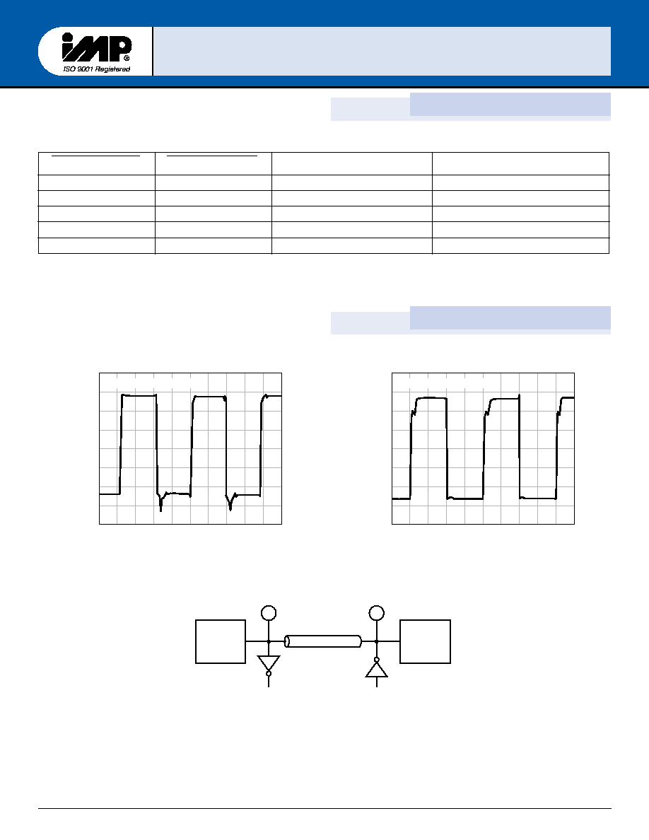
5218_03.eps
1 Meter, AWG 28
IMP5218
Receiver
Driver
IMP5218
Figure 1. Receiving Waveform ≠ 20MHz
Figure 2. Driving Waveform ≠ 20MHz
IMP5
IMP5
1
1
1
1
1/5
1/5
1
1
1
1
2
2
IMP52
IMP52
1
1
8
8
© 2000 IMP, Inc.
Data Communications
5
1
T
C
E
N
N
O
C
S
I
D
2
T
C
E
N
N
O
C
S
I
D
s
t
u
p
t
u
O
t
n
e
r
r
u
C
t
n
e
c
s
e
i
u
Q
H
H
d
e
l
b
a
n
E
A
m
6
H
L
d
e
l
b
a
n
E
A
m
6
L
H
d
e
l
b
a
n
E
A
m
6
L
L
d
e
l
b
a
s
i
D
e
c
n
a
d
e
p
m
I
h
g
i
H
/
5
7
3
µ
A
n
e
p
O
n
e
p
O
d
e
l
b
a
n
E
A
m
6
s
p
e
.
4
0
t
_
8
1
2
5
Table 1. Power Up/ Power Down Function Table
Application Information
Typical Characteristics
Line Voltage (V)
Time (250ns/Div.)
5218_04.eps
≠0.5
GND
0.5
1.5
2.5
1.0
2.0
3.5
3.0
Frequency = 1.03844MHz
Line Voltage (V)
Time (250ns/Div.)
5218_05.eps
≠0.5
GND
0.5
1.5
2.5
1.0
2.0
3.5
3.0
Frequency = 1.00266MHz
Figure 4. Receiving Waveform
Figure 5. Driving Waveform
5218_06.eps
6 Meter, 92
75C08
75C08
Figure 4
Figure 5
IMP5218
Receiver
Driver
IMP5218
Figure 6. End-Driven Cable
IMP5
IMP5
1
1
1
1
1/5
1/5
1
1
1
1
2
2
IMP52
IMP52
1
1
8
8