 | –≠–ª–µ–∫—Ç—Ä–æ–Ω–Ω—ã–π –∫–æ–º–ø–æ–Ω–µ–Ω—Ç: QS4A110 | –°–∫–∞—á–∞—Ç—å:  PDF PDF  ZIP ZIP |

1
IDTQS4A110
HIGH-PERFORMANCE CMOS TWO-CHANNEL 5PST SWITCH
INDUSTRIAL TEMPERATURE RANGE
AUGUST 2000
2000 Integrated Device Technology, Inc.
DSC-5554/1
c
INDUSTRIAL TEMPERATURE RANGE
FEATURES:
∑ Low ON resistance: r
DS
(
ON
) = 5
∑ Wide bandwidth: 1.8GHz (-3dB point)
∑ Crosstalk: 100dB at 50KHz, -70dB at 5MHz, -50dB at 30MHz
∑ Off-isolation: -70dB at 50KHz, -45dB at 5MHz, -40dB at
30MHz
∑ Single 5V supply
∑ Bidirectional
∑ TTL-compatible control inputs
∑ Ultra-low quiescent current: 3
µµ
µµ
µA
∑ Switch turn on time of 6.5ns
∑ Available in QSOP package
The IDT logo is a registered trademark of Integrated Device Technology, Inc.
APPLICATIONS:
∑ High-speed video signal switching/routing
∑ HDTV-quality video signal routing
∑ Audio signal switching/routing
∑ Data acquisition
∑ ATE systems
∑ Telecomm routing
∑ Token Ring transceivers
∑ High-speed networking
FUNCTIONAL BLOCK DIAGRAM
IDTQS4A110
QUICKSWITCH
Æ
PRODUCTS
HIGH-PERFORMANCE CMOS
TWO CHANNEL 5PST SWITCH
DESCRIPTION:
The QS4A110 is a high-performance CMOS two-channel 5PST switch
with 3-state outputs. The low ON resistance of the QS4A110 allows inputs
to be connected to outputs with low insertion loss and high bandwidth.
The QS4A110, with 1.8GHz bandwidth, is ideal for high-performance
video signal switching, audio signal switching, and telecomm routing
applications. Low power dissipation makes this device ideal for battery
operated and remote instrumentation applications.
The QS4A110 is offered in the QSOP package which has several
advantages over conventional packages such as PDIP and SOIC, includ-
ing:
∑ Reduced signal delays due to denser component packaging on circuit
boards
∑ Reduced system noise due to less pin inductance
The QS4A110 is characterized for operation at -40∞C to +85∞C.
CO NTRO L
LO G IC
E
1
E
2
A
0
A
1
A
2
C
0
C
1
C
2
A
3
C
3
D
0
D
1
D
2
B
0
B
1
B
2
D
3
B
3
A
4
C
4
D
4
B
4

2
INDUSTRIAL TEMPERATURE RANGE
IDTQS4A110
HIGH-PERFORMANCE CMOS TWO-CHANNEL 5PST SWITCH
PIN CONFIGURATION
QSOP
TOP VIEW
Symbol
Description
Max
Unit
V
TERM
(2)
Supply Voltage to Ground
≠0.5 to +7
V
V
TERM
(3)
DC Switch Voltage V
S
0 to +7
V
--
Analog Input Voltage
0 to +7
V
V
TERM
(3)
DC Input Voltage V
IN
0 to +7
V
V
AC
AC Input Voltage (pulse width
20ns)
≠3
V
I
OUT
DC Output Current
120
mA
P
MAX
Maximum Power Dissipation
0.7
W
T
STG
Storage Temperature
≠65 to +150
∞C
ABSOLUTE MAXIMUM RATINGS
(1)
Pin Names
I/O
Description
Ax, Bx
I/O
Ports A, B
Cx, Dx
I/O
Ports C, D
E
1
-E
2
I
Enable
PIN DESCRIPTION
NOTES:
1. Stresses greater than those listed under ABSOLUTE MAXIMUM RATINGS may cause
permanent damage to the device. This is a stress rating only and functional operation
of the device at these or any other conditions above those indicated in the operational
sections of this specification is not implied. Exposure to absolute maximum rating
conditions for extended periods may affect reliability.
2. V
CC
terminals.
3. All terminals except V
CC
.
NOTE:
1. H = HIGH Voltage Level
L = LOW Voltage Level
E
1
E
2
Ax, Cx I/Os
Bx, Dx I/Os
H
H
Disconnected
Disconnected
L
H
Ax = Cx
Disconnected
H
L
Disconnected
Bx = Dx
L
L
Ax = Cx
Bx = Dx
FUNCTION TABLE
(1)
E
1
C
0
A
0
A
1
C
1
C
2
A
2
A
3
C
3
C
4
A
4
GND
V
CC
D
4
B
4
B
3
D
3
D
2
B
2
B
1
D
1
D
0
B
0
E
2
1
2
3
4
5
6
7
8
9
10
11
12
24
23
22
21
20
19
18
17
16
15
14
13
3
IDTQS4A110
HIGH-PERFORMANCE CMOS TWO-CHANNEL 5PST SWITCH
INDUSTRIAL TEMPERATURE RANGE
DC ELECTRICAL CHARACTERISTICS OVER OPERATING RANGE
Following Conditions Apply Unless Otherwise Specified:
Industrial: T
A
= ≠40∞C to +85∞C, V
CC
= 5V ± 5%
POWER SUPPLY CHARACTERISTICS
Symbol
Parameter
Test Conditions
Max.
Unit
I
CC
Supply Current
V
CC
= Max., V
IN
= GND or V
CC
3
µA
Symbol
Parameter
Test Conditions
Min.
Typ.
(1)
Max.
Unit
Analog Switch
V
IN
Analog Signal Range
(2)
≠0.5
1
Vcc - 1
V
r
DS
(
ON
)
Drain-source ON resistance
(2,3)
Vcc = Min., V
IN
= 0V
, I
ON
= 30mA
--
5
7
Vcc = Min., V
IN
= 2.4V
, I
ON
= 15mA
--
13
17
I
C(OFF)
Channel Off Leakage Current
Ax, Bx = Vcc or 0V; Cx, Dx = 0V or Vcc; E = Vcc
--
1
--
nA
I
C(ON)
Channel On Leakage Current
Ax = Bx = 0V
--
1
--
nA
(each channel is turned on sequentially)
Digital Control
V
IH
Input HIGH Voltage
Guaranteed Logic HIGH for Control Pins
2
--
--
V
V
IL
Input LOW Voltage
Guaranteed Logic LOW for Control Pins
--
--
0.8
V
Dynamic Characteristics
t
ON(E)
Enable Turn-On Time
R
L
= 1K
, C
L
= 100pF
0.5
--
6
ns
E to Ax, Bx, Cx, or Dx
(See Switching Time)
t
OFF(E)
Enable Turn-Off Time
R
L
= 1K
, C
L
= 100pF
0.5
--
6.5
ns
E to Ax, Bx, Cx, or Dx
(See Switching Time)
t
PD
Group Delay
(2,4a)
R
L
= 1K
, C
L
= 100pF
--
--
250
ps
f
3dB
-3dB Bandwidth
V
IN
= 0 to 1V, 1Vp-p, R
L
= 75
--
1.8
--
GHz
Off-isolation
V
IN
= 0 to 1V, 1Vp-p, R
L
= 75
, f = 5.5MHz
--
-45
--
dB
X
TALK
Crosstalk
V
IN
= 0 to 1V, 1Vp-p, R
L
= 75
, f = 5.5MHz
--
-70
--
dB
C
(OFF)
Switch Off Capacitance
E = Vcc, V
IN
= V
OUT
= 0V
--
5
--
pF
C
(ON)
Switch On Capacitance
E = 0V, V
IN
= V
OUT
= 0V
--
10
--
pF
Q
CI
Charge Injection
--
1.5
--
pC
NOTES:
1. Typical values are at V
CC
= 5.0V, T
A
= 25∞C.
2. Max value is guaranteed but not production tested.
3. Measured by voltage drop between A and C pins or B and D pins at indicated current through the switch. ON resistance is determined by the lower of the voltages on the
two (A, C, or B, D) pins.
4. The bus switch contributes no group delay other than the RC delay of the ON resistance of the switch and load capacitance. Group delay of the bus switch, when used
in a system, is determined by the driving circuit on the driving side of the switch and its interaction with the load on the driven side.
4
INDUSTRIAL TEMPERATURE RANGE
IDTQS4A110
HIGH-PERFORMANCE CMOS TWO-CHANNEL 5PST SWITCH
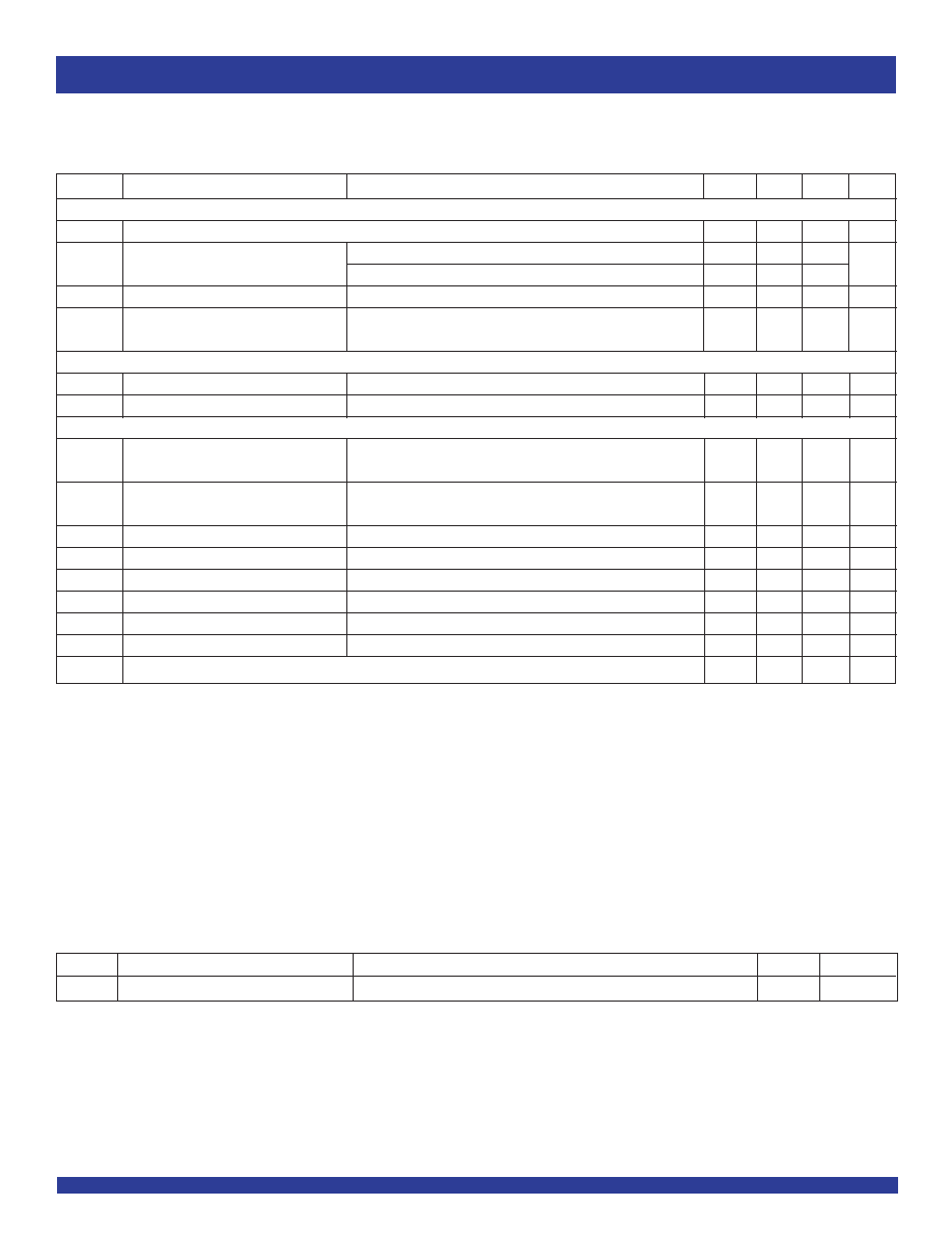
TYPICAL CHARACTERISTICS
NOTES:
1. Crosstalk = 20 log |V
O
/V
S
|
2. Off-isolation = 20 log |V
O
/V
S
|
NOTES:
1. Crosstalk = 20 log |V
O
/V
S
|
2. Off-isolation = 20 log |V
O
/V
S
|
NOTES:
1. Crosstalk = 20 log |V
O
/V
S
|
2. Off-isolation = 20 log |V
O
/V
S
|
NOTE:
1. Insertion Loss = 20 log |V
O
/V
S
|
Off-isolation and Crosstalk vs. Frequency
Off-isolation and Crosstalk vs. Frequency
Off-isolation and Crosstalk vs. Frequency
Insertion Loss vs. Frequency
1K
10K
100K
1M
10M
100M
1G
10G
Freq uen cy (H z)
(
d
B
)
Crosstalk
Off-isolation
V
C C
= 5V
R
L
= 75
180
150
120
90
60
30
0
500M
Frequency (Hz)
(
d
B
)
Crosstalk
600M
700M
400M
300M
200M
100M
Off-isolation
60
50
40
30
20
10
0
V
CC
= 5V
R
L
= 75
50K
Freq u en cy (H z)
(
d
B
)
60K
70K
40K
30K
20K
10K
Off-isolation
Crosstalk
160
140
120
100
80
60
40
V
C C
= 5V
R
L
= 75
2
1
0
1
2
3
4
1K
10K
100K
1 M
10 M
100 M
1 G
10 G
5
6
F req u en cy (H z)
(
d
B
)
V
C C
= 5V
R
L
= 7 5
5
IDTQS4A110
HIGH-PERFORMANCE CMOS TWO-CHANNEL 5PST SWITCH
INDUSTRIAL TEMPERATURE RANGE
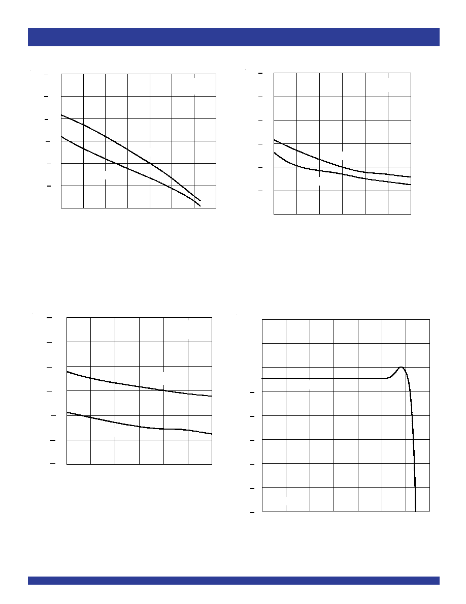
TYPICAL CHARACTERISTICS (CONTINUED)
Insertion Loss vs. Frequency
On-Resistance vs. V
IN
NOTE:
1. Insertion Loss = 20 log |V
O
/V
S
|
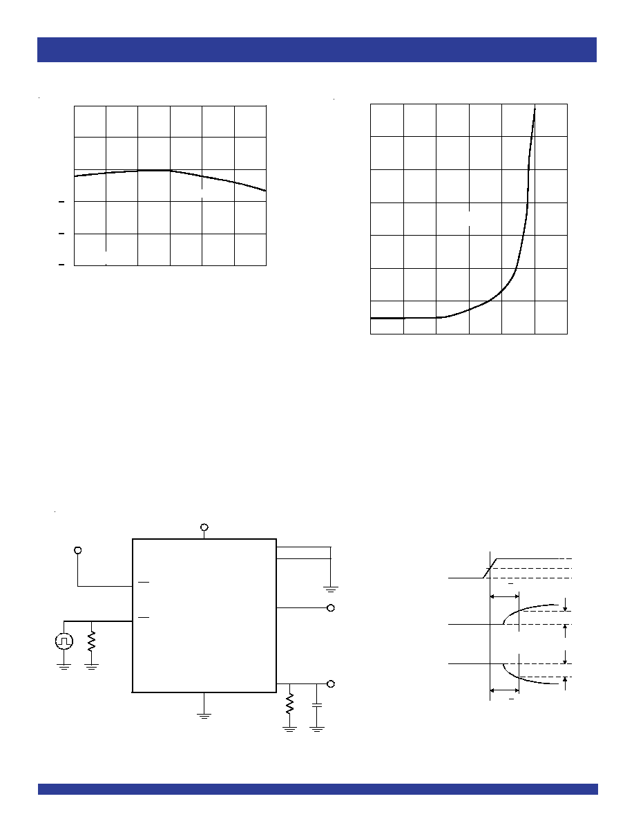
Switching Time
TEST CIRCUITS
16
14
12
10
8
0.0
0.5
1.0
1.5
2.0
2.5
3.0
6
4
V
IN
(Volts)
r
D
S
(
O
n
)
-
D
r
a
i
n
S
o
u
r
c
e
O
n
-
r
e
s
i
s
t
a
n
c
e
(
)
V
CC
= 4.75V
18
R
ON
LINK
2
1
0
1
2
3
1G
Freq uen cy (H z)
(
d
B
)
1.1G
700M
800M
900M
500M
600M
V
C C
= 5V
R
L
= 75
A0-A3
C0-C3
GND
5V
V
OUT
500
50 pF
Vcc
5V
E2
E1
5V
500
V
IN
QS4A110
CONTROL
INPUT
OUTPUT
3.0V
1.5V
0V
t
ON(E)
0.3V
t
OFF(E)
0.3V
OUTPUT
A4
C4
6
INDUSTRIAL TEMPERATURE RANGE
IDTQS4A110
HIGH-PERFORMANCE CMOS TWO-CHANNEL 5PST SWITCH
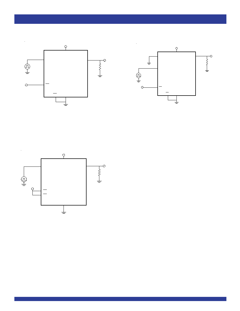
Insertion Loss
NOTES:
1. Insertion Loss = 20 log |V
O
/V
S
|
2. All unused pins are grounded.
Crosstalk
NOTES:
1. Crosstalk = 20 log |V
O
/V
S
|
2. All unused pins are grounded.
Off-Isolation
NOTE:
1. Off-isolation = 20 log |V
O
/V
S
|
TEST CIRCUITS (CONTINUED)
GND
V
OUT
Vcc
5V
E2
5V
V
S
QS4A110
A4
E1
C4
R
L
=
75
GND
V
OUT
Vcc
5V
E2
5V
V
S
QS4A110
B4
E1
C1
A1
R
L
=
75
GND
V
OUT
Vcc
5V
E1
E2
5V
V
S
QS4A110
A1
C1
R
L
=
75
7
IDTQS4A110
HIGH-PERFORMANCE CMOS TWO-CHANNEL 5PST SWITCH
INDUSTRIAL TEMPERATURE RANGE
ORDERING INFORMATION
CORPORATE HEADQUARTERS
for SALES:
for Tech Support:
2975 Stender Way
800-345-7015 or 408-727-6116
logichelp@idt.com
Santa Clara, CA 95054
fax: 408-492-8674
(408) 654-6459
www.idt.com
IDTQS
XXXXX
XX
Package
Device Type
Quarter Size Outline Package
Q
4A110
High Performance CMOS Two Channel 5PST Switch