 | –≠–Ľ–Ķ–ļ—ā—Ä–ĺ–Ĺ–Ĺ—č–Ļ –ļ–ĺ–ľ–Ņ–ĺ–Ĺ–Ķ–Ĺ—ā: IDT77V400 | –°–ļ–į—á–į—ā—Ć:  PDF PDF  ZIP ZIP |
1 of 26
March 31, 2001
2001 Integrated Device Technology, Inc.
DSC 3606/6
SwitchStar
TM
ATM Cell Based
8 x 8 1.2Gbps non-blocking
Integrated Switching Memory
Features List
Features List
Features List
Features List
!
Single chip supports an 8 x 8 port switch at 155Mbps per
port
!
Central Memory Architecture eliminates Head-of-Line
Blocking by sharing the memory array with all ports
!
Low power dissipation
≠ 330mW (typ.)
!
Data Path Interface (DPI) provides configurable Input and
Output ports; up to 8 receive and 8 transmit ports at
155Mbps
!
Supports data rates up to 1.2Gbps with a 32-bit wide port
configuration; 155Mbps per 4-bit port
!
Can be cascaded for larger switch configurations
!
Fast Input/Output port cycle times
!
Expander and Concentrator function is fully supported by
the Input and Output port configuration options
!
8192 cells (52 to 56 bytes each) of on-chip buffer memory
capacity
!
Configurable cell lengths of 52, 53, 54, 55, or 56 bytes can
be independently chosen for Input and Output ports
!
Byte Addition or Byte Subtraction for x4/x8 to x16/x32
conversion capability
!
Internal header Cyclical Redundancy Check (CRC) and
generation logic on-chip
!
Header modification, pre-pend, and post-pend operations
available as well as Multicasting and Broadcasting
capability
!
High-bandwidth control port for queue controller system
block, up to 36 MHz cycle time
!
Can be used with the companion IDT77V500 Switch
Controller or custom logic for traffic management
!
Industrial temperature range (-40įC to +85įC) is available
!
Single +3.3V Ī 300mV power supply
!
Available in an 208-pin Plastic Quad Flat Pack (PQFP) and
256-ball BGA
Block Diagram
Block Diagram
Block Diagram
Block Diagram
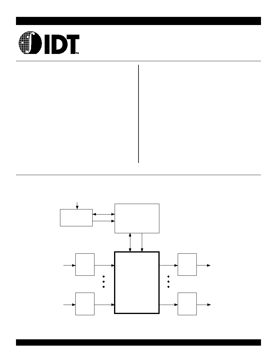
Figure 1 Typical 8x8 Switch Configuration using the IDT77V400 Switching Memory
SwitchStar and the IDT logo are registered trademarks of Integrated Device Technology, Inc.
8-bit Processor/
Call Setup
Manager
IDT77V500
Switch
Controller
IDT77V400
Switching
Memory
155Mbps
PHY
Port 0
Port 0
Port 7
Port 7
Control
Control
Data
Data
External Interface
for Global Setup
and Control
3606 drw 01
or IDT77V550
155Mbps
PHY
155Mbps
PHY
155Mbps
PHY
,
IDT77V400

2 of 26
March 31, 2001
IDT77V400
Description
Description
Description
Description
The IDT77V400 ATM Cell Based Switching Memory provides the
logic and memory necessary to perform high-speed buffering and
switching operations on ATM cell data. A single IDT77V400 provides a
cost effective switching element to implement an 8 x 8 155Mbps switch
with 1.2Gbps total switching bandwidth. The user configurable data
ports provide an aggregate bandwidth of 1.2Gbps for both receive and
transmit functions, and the cell lengths are user programmable to up to
56 bytes.
The memory provides storage for 8192 ATM cells, each of which can
be as large as 56-bytes in length. The main cell memory is implemented
as a Buffer Memory array, and an on-chip cell address counter keeps
track of cell refresh requirements. There are also sixteen double-buff-
ered Serial Access Memories (SAM); eight for receiving and eight for
transmitting the ATM cells.
The input data ports and output data ports are configurable from
eight ports of 4-bits at 155Mbps each up to one 32-bit wide port at
1.2Gbps. The sixteen data ports are asynchronous with respect to each
other, and each port provides an independent data clock and cell
framing signal for start of cell indication. The SAMs are double-buffered
for each input and each output port to allow one cell to be transferred to
or from the internal memory while that data port continues to receive or
transmit a second cell. The cell framing and data clock signals imple-
ment a simple handshaking and synchronization protocol which allows
multiple Switching Memories to be connected to construct larger switch
arrays without requiring additional hardware.
The control interface of the IDT77V400 includes a 6-bit Command
Bus (CMD0-5), a 32-bit Control Data Bus (IOD0-31), a Chip Select pin
(CS), a 4-bit Address field (ADDR0-3), a RESET pin, an Output Enable
pin (OE), a Control Enable pin (CTLEN) and a CRCERR pin. All control
operations are synchronized with respect to the System Clock (SCLK),
with the exception of RESET, CTLEN, and OE, which are fully asynchro-
nous.
The internal configuration register of the IDT77V400 can be
accessed through the Control Data Bus to define the cell length and the
input and output data port configurations. Internal error and status regis-
ters contain status information regarding each SAM and are accessible
via the Control Data Bus (IOD0-31). Input SAM full or Output SAM
empty status for all SAMs may be obtained in one access operation.
Additional information regarding the reception of short or long cells and
Input SAM overflow may also be obtained through the Control Data Bus.
The command set of the Switching Memory provides functions for
storing cells in the shared memory, loading Output SAMs, polling the
status of the data ports, retrieving and storing original or modified
header bytes and pre-pend or post-pend bytes, and refreshing the cell
memory. Header CRC errors are indicated by a LOW CRCERR pin; the
CRC comparison byte may also be accessed via the status register,
which indicates the IPort on which the error was detected. A new CRC
can be generated upon storing a new header in the PHEC command.
Cell headers may be modified upon cell reception at the input ports or
upon cell transmit at the output ports. User defined pre-pend and post-
pend bytes may also be stored, retrieved, and modified through the
Control Data Bus.
The IDT77V400 has a generic control interface which supports a
variety of queuing disciplines. By maintaining the memory control in an
external controller, system level switching performance may be modified
over time as requirements change. In normal operation, the Switching
Memory port status is polled by the control function through the Control
Data Bus. Upon receiving a cell, the control function can retrieve the
header, check the CRC result, and store a new header if needed prior to
moving the cell to the shared memory. Pre-pended or post-pended
bytes may also be added or retrieved during this time. The output ports
are polled at the same time to determine when to send new cells to the
Output SAMs. The cell lengths of the input ports do not need to be the
same as the output port cell lengths, although all input ports and output
ports respectively must be configured to the same cell length.
Please refer to the SwichStar User Manual for additional feature
details and implementation information.
The IDT77V400 is fully 3.3V LVTTL compatible, and is packaged in
an 208-pin Plastic Quad Flatpack (PQFP) and a 256-ball BGA.

3 of 26
March 31, 2001
IDT77V400
Figure 2 Functional Block Diagram
Figure 3 Input and Output Edit Buffer Block Diagram
OE
IOD0-31
32
CRC Logic
Edit Buffer
Control
Mode Control
and CRC
Config.
Cntl.
Config.
Nibble Counters
Pointer Decode + Control
Output SAM Port 0
Output SAM Port 6
Output SAM Port 7
Output
Header
Output
Edit Buffer
OFRM
and OCLK
Control
Output
Latches
and
Buffers
Buffer Memory
(8192 ATM Cells)
Addr
Memory
Control
Logic
Input
Latches
and
Buffers
Nibble Counters,
Pointer Decode + Control
Config.
Config.
Port
Status
Error
Register
Status
Register
Configuration
Register
Control Interface and
Command Control
IFRM
and ICLK
Control
OCLK0-7
OFRM0-7
OP0D0-3
OP1D0-3
OP2D0-3
OP3D0-3
OP4D0-3
OP5D0-3
OP6D0-3
OP7D0-3
CRCERR
CS
ADDR0-3
4
RESET
SCLK
CMD0-5
6
Config.
4
4
4
IP0D0-3
IP1D0-3
IP2D0-3
IP3D0-3
IP4D0-3
IP5D0-3
IP6D0-3
IP7D0-3
ICLK0-7
IFRM0-7
4
8
8
8
8
4
4
4
4
4
4
4
4
8
8
4
4
4
3606 drw 02
Cntl.
4
4
4
4
4
4
4
Input
Edit Buffer
CTLEN
4
4
4
4
4
4
4
4
4
4
4
4
ABYTE
SBYTE
Cntl.
Input SAM Port 0
Input SAM Port 7
Refresh
Control
1
1
IOD0-31
Random Access Cell Memory
Input SAM Port 1
INPUT
TRANSFER BUS
Bits 0-71
3606 drw 03
OUTPUT
DRAM BUS
Bits 0-71
OUTPUT
TRANSFER BUS
Bits 0-71
CLEAR
BYTE-PUT-PROTECT
byte 0
byte 1
byte 2
byte 3
HEC
GEN
CRC
BYTE
OR - P/P
OR - HEADER
XOR
.
[second word]
[first word]
MUX
32
32
32
IOD BUS Bits 0 - 31
MUX
32
[first word]
[second word]
HEC
32
32
32
32
8
8
COMPARE
8
8
OUTPUT EDIT BUFFER
8
32
CRC error
72
(from ISAM)
(to OSAM)
GEN
CRC
To DRAM
INPUT EDIT BUFFER

4 of 26
March 31, 2001
IDT77V400
Package Diagram
Package Diagram
Package Diagram
Package Diagram
All V
CC
/V
CCQ
pins must be connected to power supply. All V
SS
pins must be connected to ground supply. Package body is approximately 28mm x
28mm x 3.4mm.
1
This package code is used to reference the package diagram.
2
This text does not indicate orientation of the actual part marking.
1
2
3
4
5
6
7
8
9
10
11
12
13
14
15
16
17
18
19
20
21
22
23
24
25
26
27
28
29
30
31
32
33
34
35
36
37
38
39
40
41
42
43
44
45
46
47
48
49
50
51
52
5
3
5
4
5
5
5
6
5
7
5
8
5
9
6
0
6
1
6
2
6
3
6
4
6
5
6
6
6
7
6
8
6
9
7
0
7
1
7
2
7
3
7
4
7
5
7
6
7
7
7
8
7
9
8
0
8
1
8
2
8
3
8
4
8
5
8
6
8
7
8
8
8
9
9
0
9
1
9
2
9
3
9
4
9
5
9
6
9
7
9
8
9
9
1
0
0
1
0
1
1
0
2
1
0
3
1
0
4
156
155
154
153
152
151
150
149
148
147
146
145
144
143
142
141
140
139
138
137
136
135
134
133
132
131
130
129
128
127
126
125
124
123
122
121
120
119
118
117
116
115
114
113
112
111
110
109
108
107
106
105
2
0
8
2
0
7
2
0
6
2
0
5
2
0
4
2
0
3
2
0
2
2
0
1
2
0
0
1
9
9
1
9
8
1
9
7
1
9
6
1
9
5
1
9
4
1
9
3
1
9
2
1
9
1
1
9
0
1
8
9
1
8
8
1
8
7
1
8
6
1
8
5
1
8
4
1
8
3
1
8
2
1
8
1
1
8
0
1
7
9
1
7
8
1
7
7
1
7
6
1
7
5
1
7
4
1
7
3
1
7
2
1
7
1
1
7
0
1
6
9
1
6
8
1
6
7
1
6
6
1
6
5
1
6
4
1
6
3
1
6
2
1
6
1
1
6
0
1
5
9
1
5
8
1
5
7
IDT77V400DS
DS208-1
1
208-Pin PQFP
Top View
2
NC
VCC
VSS
VSS
IOD0
IOD1
IOD2
IOD3
IOD4
IOD5
IOD6
IOD7
IOD8
IOD9
VCC
VCC
IOD10
IOD11
IOD12
IOD13
IOD14
IOD15
IOD16
IOD17
IOD18
IOD19
IOD20
VSS
VSS
IOD21
IOD22
IOD23
IOD24
IOD25
IOD26
IOD27
IOD28
IOD29
IOD30
IOD31
VCC
VCC
VSS
VSS
OP0D3
OP0D2
OP0D1
OP0D0
VCC
VCC
VSS
NC
N
C
N
C
V
C
C
Q
V
C
C
O
P
2
D
3
O
P
2
D
2
O
P
2
D
1
O
P
2
D
0
V
S
S
V
S
S
O
P
4
D
3
O
P
4
D
2
O
P
4
D
1
O
P
4
D
0
V
C
C
V
C
C
O
P
6
D
3
O
P
6
D
2
O
P
6
D
1
O
P
6
D
0
V
S
S
O
F
R
M
0
O
F
R
M
1
O
F
R
M
2
O
F
R
M
3
O
F
R
M
4
O
F
R
M
5
O
F
R
M
6
O
F
R
M
7
V
S
S
V
C
C
V
C
C
V
S
S
O
C
L
K
0
O
C
L
K
1
O
C
L
K
2
O
C
L
K
3
O
C
L
K
4
O
C
L
K
5
O
C
L
K
6
O
C
L
K
7
C
T
L
E
N
O
E
V
S
S
O
P
7
D
3
O
P
7
D
2
O
P
7
D
1
O
P
7
D
0
V
C
C
V
C
C
V
S
S
N
C
NC
VSS
VCC
IP3D0
IP3D1
IP3D2
IP3D3
IP5D0
IP5D1
IP5D2
IP5D3
IP7D0
IP7D1
IP7D2
IP7D3
VSS
VCC
CS
CMD5
CMD4
CMD3
CMD2
CMD1
CMD0
SCLK
ADDR3
ADDR2
ADDR1
ADDR0
VSS
VCC
VSS
OP1D0
OP1D1
OP1D2
OP1D3
VCC
VCC
OP3D0
OP3D1
OP3D2
OP3D3
VSS
VSS
OP5D0
OP5D1
OP5D2
OP5D3
VCC
VCCQ
NC
NC
V
C
C
Q
S
B
Y
T
E
A
B
Y
T
E
C
R
C
E
R
R
V
C
C
V
S
S
I
P
6
D
0
I
P
6
D
1
I
P
6
D
2
I
P
6
D
3
I
P
4
D
0
I
P
4
D
1
I
P
4
D
2
I
P
4
D
3
V
S
S
V
C
C
I
P
2
D
0
I
P
2
D
1
I
P
2
D
2
I
P
2
D
3
I
P
0
D
0
I
P
0
D
1
I
P
0
D
2
I
P
0
D
3
V
C
C
V
S
S
I
F
R
M
7
I
F
R
M
6
I
F
R
M
5
I
F
R
M
4
I
F
R
M
3
I
F
R
M
2
I
F
R
M
1
I
F
R
M
0
I
C
L
K
7
I
C
L
K
6
I
C
L
K
5
I
C
L
K
4
I
C
L
K
3
I
C
L
K
2
I
C
L
K
1
I
C
L
K
0
R
E
S
E
T
V
C
C
V
S
S
I
P
1
D
0
I
P
1
D
1
I
P
1
D
2
I
P
1
D
3
N
C
N
C
N
C
3606 drw 04

5 of 26
March 31, 2001
IDT77V400
Package Diagram
Package Diagram
Package Diagram
Package Diagram
(1,2,3)
(1,2,3)
(1,2,3)
(1,2,3)
BC256-1 BGA
BC256-1 BGA
BC256-1 BGA
BC256-1 BGA
Note:
1. All V
CC
pins must be connected to power supply.
2. All V
SS
pins must be connected to ground supply.
3. Package body is approximately 17mm x 17mm x 1.4mm.
E16
IP
7D0
D16
IP
5D0
C16
IP
3D3
B16
IP
3D1
A16
IP
3D0
A15
IP
1D1
B15
IP
1D3
C15
IP
3D2
D15
IP
5D1
E15
IP
5D3
E14
IP
7D1
D14
IP
5D2
D13
V
CC
C12
ICLK
5
C14
IP
1D2
B14
IP
1D0
A14
RESET
A12
ICLK
4
B12
ICLK
3
C11
IFRM
0
D12
V
CC
D11
V
CC
C10
IFRM
3
B11
ICLK
6
A11
ICLK
7
D8
V
CC
C8
IFRM
7
A9
IFRM
4
D9
V
CC
C9
IFRM
6
B9
IFRM
5
D10
V
CC
C7
IP
0D1
B8
IP
0D2
A8
IP
0D3
B13
ICLK
0
A13
ICLK
1
A10
IFRM
2
D7
V
CC
B7
IP
2D3
A7
IP
0D0
B6
IP
2D0
C6
IP
2D2
D6
V
CC
A5
IP
4D2
B5
IP
4D1
C5
IP
4D3
D5
V
CC
A4
IP
6D3
B4
IP
6D2
C4
IP
4D0
D4
V
CC
A3
IP
6D1
B3
IP
6D0
C3
IOD
0
D3
IOD
5
D2
IOD
4
C2
IOD
3
B2
SBYTE
A2
C R C E R R
A1
ABYTE
B1
IOD
1
C1
IOD
2
D1
IOD
6
E1
IOD
8
E2
IOD
7
E3
IOD
9
E4
V
CC
F1
IOD
11
F2
IOD
10
F3
IOD
12
F4
V
CC
G1
IOD
14
G2
IOD
13
G3
IOD
15
G4
V
CC
H1
IOD
17
H2
IOD
16
H3
IOD
18
H4
V
CC
J1
IOD
20
J2
IOD
21
J3
IOD
19
J4
V
CC
K1
IOD
23
K2
IOD
24
K3
IOD
22
K4
V
CC
L1
IOD
26
L2
IOD
27
L3
IOD
25
L4
V
CC
M1
IOD
29
M2
IOD
30
M3
IOD
28
M4
V
CC
N1
OP
0D3
N2
OP
0D2
N3
IOD
31
N4
V
CC
P1
OP
0D1
P2
OP
0D0
P3
NC
P4
OP
2D0
R1
NC
R2
NC
R3
OP
2D3
R4
OP
2D1
T1
NC
T2
NC
T3
OP
2D2
T4
OP
4D3
P5
OP
4D0
R5
OP
4D2
P12
OCLK
6
P8
OFRM
4
P9
OFRM
5
R8
OFRM
2
T8
OFRM
3
P10
OCLK
0
T11
OCLK
4
P11
OCLK
3
R12
C T L E N
T12
OCLK
7
P13
O E
P7
OFRM
1
R13
OP
7D3
T13
OP
7D2
R6
OP
6D3
T5
OP
4D1
T14
OP
7D1
R14
OP
7D0
P14
NC
P15
OP
5D3
R15
NC
T15
NC
T16
NC
R16
NC
P16
OP
5D2
N16
OP
3D3
N15
OP
5D1
N14
OP
5D0
M16
OP
3D0
M15
OP
3D2
M14
OP
3D1
L16
OP
1D1
L15
OP
1D3
L14
OP
1D2
K16
ADDR
1
K15
OP
1D0
K14
ADDR
0
J16
ADDR
3
J15
ADDR
2
J14
SCLK
H16
CMD
1
H15
CMD
2
H14
CMD
0
G16
CMD
4
G15
CMD
5
G14
CMD
3
F16
IP
7D3
F14
C S
F15
IP
7D2
R9
OFRM
7
R11
OCLK
5
T6
OP
6D2
T9
OFRM
6
A6
IP
2D1
B10
IFRM
1
C13
ICLK
2
P6
OP
6D1
R10
OCLK
2
R7
OP
6D0
T10
OCLK
1
T7
OFRM
0
E5
V
CC
E6
V
CC
E7
V
SS
E8
V
SS
E9
V
SS
E10
V
SS
E11
V
CC
E12
V
CC
E13
V
CC
F5
V
CC
F6
V
SS
F8
V
SS
F9
V
SS
F10
V
SS
F12
V
CC
F13
V
CC
G5
V
SS
G6
V
SS
G7
V
SS
G8
V
SS
G9
V
SS
G10
V
SS
G11
V
SS
G12
V
SS
G13
V
CC
H5
V
SS
H6
V
SS
H7
V
SS
H8
V
SS
H9
V
SS
H10
V
SS
H11
V
SS
H12
V
SS
H13
V
CC
J5
V
SS
J6
V
SS
J7
V
SS
J8
V
SS
J9
V
SS
J10
V
SS
J11
V
SS
J12
V
SS
J13
V
CC
K5
V
SS
K6
V
SS
K7
V
SS
K8
V
SS
L5
V
CC
L6
V
SS
L7
V
SS
L8
V
SS
M5
V
CC
M6
V
CC
M7
V
SS
M8
V
SS
N5
V
CC
N6
V
CC
N7
V
CC
N8
V
CC
K9
V
SS
K10
V
SS
K11
V
SS
K12
V
SS
L9
V
SS
L10
V
SS
L11
V
SS
L12
V
CC
M9
V
SS
M10
V
SS
M11
V
CC
M12
V
CC
N9
V
CC
N10
V
CC
N11
V
CC
N12
V
CC
K13
V
CC
L13
V
CC
M13
V
CC
N13
V
CC
F7
V
SS
F11
V
SS
3606 drw 04a
,

6 of 26
March 31, 2001
IDT77V400
Pin Description - PQFP Package
Pin Description - PQFP Package
Pin Description - PQFP Package
Pin Description - PQFP Package
Pin Number
Symbol Type
Description
132
SCLK
I
System clock: All bus control signals (CMD0-5, CS, IOD0-31, CRCERR) except OE are synchronous with respect to
SCLK. Control commands are registered on the positive edge of SCLK. The SCLK period must be less than or equal to
200ns during normal operation. Data Port signals are asynchronous with respect to SCLK.
139
CS
I
Chip Select: Synchronous input which must be LOW at the rising edge of SCLK to enable the Command Bus CMD0-5.
Instructions are a NOP when CS is HIGH at the SCLK positive edge.
133-138
CMD0-5
I
Command Bus: Synchronized to SCLK, instructions to be executed by the memory are transferred across this 6-bit
bus. CMD5 is the MSb of the Command Bus.
95
OE
I
Output Enable: Asynchronous input that enables all outputs when asserted LOW. All outputs are High-Z when OE is
HIGH. IOD0-31 and CRCERR may also be set to High-Z by a HIGH CTLEN bit in the configuration register or a HIGH
CTLEN pin.
166
RESET
I
Reset: When asserted HIGH, the signal asynchronously allows the initialization of the registers and internal signals of
the IDT77V400. RESET should be asserted HIGH and OE should be held HIGH upon power-up for the external con-
troller to execute the initialization and insure proper system operation.
128-131
ADDR0-3
I
Chip Address: All ADDR inputs must OR the address in the configuration register bits 26-29 and then must match
1OD13-16 one cycle after the Store or Load command for selection to allow a Store or Load memory cycle to be exe-
cuted (full flag is cleared regardless of match, and empty must match before clear). ADDR3 is the MSb of the device
address bits.
5-14, 17-27, 30-40
IOD0-31
I/O
Control Data Bus: Synchronous with SCLK. Used for external data transfer for the header pre/post-pend bytes, config-
uration register error and status registers, and the cell memory address. IOD31 is the MSb of the Control Data Bus.
205
CRCERR
O
Cyclical Redundancy Check Error: Synchronous output on the rising edge of SCLK. CRCERR asserted LOW after a
Header with CRC operation indicates that a CRC error has occurred on the previous header.
167-174
ICLK0-7
I
Input Port Clock: Synchronizes the input data IPxD(0-3) and IFRMx signal associated with the input data port on the
positive clock edge. Each ICLKx is independent of the other seven ICLKs and SCLK. The ICLKs used are determined
by the configuration register initialization (see Port Configuration Code Table). The inputting of a cell may be halted by
stopping ICLKx.
175-182
IFRM0-7
I
Input Frame: Synchronous input registered on the rising edge of ICLKx. When asserted HIGH this signal denotes the
beginning of an input cell for the associated input port. IFRMs used are determined by the configuration register during
initialization (see Port Configuration Code Table).
185-188, 160-163,
189-192, 150-153,
195-198, 146-149,
199-202, 142-145
IP(0-7)D(0-3) I
Input Data: Eight 4-bit input ports. Synchronous with the rising edge of ICLK for the associated data port. IPxD(0-3)
can be assigned to different ICLKs and IFRMs via the configuration register during initialization. The ports may be
combined in groups to increase bandwidth by factors of 155Mbps (see Port Configuration Code Table). IPxD3 is the
MSb of the nibble. Example: IP0D3 is the MSb for port 0.
86-93
OCLK0-7
I
Output Clock: Synchronizes the output data OPxD(0-3) and OFRMx signal associated output data port on the positive
clock edge. Each OCLK is independent of the other seven OCLKs and SCLK. OCLKs used are determined by the port
configuration register during initialization (see Port Configuration Code Table). The transmission of a cell may be
halted by stopping OCLKx.
74-81
OFRM0-7
I/O
Output Frame: Synchronous output on the rising edge of OCLK. The 77V400 marks the beginning of an output cell by
taking OFRM HIGH on the rising edge of OCLK. The output SAM nibble counter loads the start byte address from the
configuration register when a HIGH signal is sensed at the OFRM pin, thus re-synchronizing other chips connected to
the OFRM bus. OFRM is asserted HIGH one OCLK cycle prior to the first nibble of the cell being output from the
IDT77V400. OFRMs used are determined by the configuration register initialization (see Port Configuration Code
Table). During cell bus operations, the OFRM1-7 are redefined as CBUS1-7 for arbitration (there is no CBUS0).
45-48, 121-124, 57-
60, 115-118, 63-66,
109-112, 69-72, 97-
100
OP(0-7)D(0-3) O
Output Data: Eight 4-bit output ports. Synchronous with the rising edge of OCLK for the associated data port. OPxD(0-
3) can be assigned to different OCLKs and OFRMs via the configuration register. The 4 bit ports may be combined in
groups to increase the bandwidth by factors of 155Mbps (see Port Configuration Code Table). OPxD3 is the MSb of
the nibble. Example: IP0D3 is the MSb for port 0.
7 of 26
March 31, 2001
IDT77V400
Pin Description - BGA Package
Pin Description - BGA Package
Pin Description - BGA Package
Pin Description - BGA Package
94
CTLEN
I
Control Enable: When asserted LOW, with OE LOW and the CTLEN bit set LOW in the configuration register, this pin
asynchronously enables all Control interface outputs. If CTLEN is HIGH all control interface outputs will be High-Z.
206
ABYTE
I
Add Byte to Input cell: Asynchronous DC signal. If an input port is in a 4-bit or 8-bit DPI mode and ABYTE is asserted
HIGH, a dummy byte will be inserted in the ninth byte position (after the HEC byte) to support systems requiring a byte
between the last header byte and the payload (otherwise ignored). Not intended for dynamic cycling or operation.
207
SBYTE
I
Subtract Byte to Output cell: Asynchronous DC signal. When and SBYTE is asserted HIGH, the dummy byte in the
ninth byte position (after the HEC byte) will be removed prior to transmission to support output port 4-bit and 8-bit DPI
modes (otherwise ignored). Not intended for dynamic cycling or operation.
1, 52-54, 104-06,
156-59
NC
--
No Connect
2, 15-16, 41-42, 49-
50, 56, 67-68, 83-84,
101-02, 108, 119-20,
126, 140, 154, 165,
184, 193, 204
VCC
Power
Power Supply (+3.3V Ī 300mV)
55, 107, 208
VCCQ
Power
Output Power Supply (+3.3 Ī 300mV)
3-4, 28-29, 43-44,
51, 61-62, 73, 82, 85,
96, 103, 113-14,
125, 127, 141, 155,
164, 183, 194, 203
VSS
Power
Ground
Pin Number
Symbol Type
Description
J14
SCLK
I
System clock: All bus control signals (CMD0-5, CS, IOD0-31, CRCERR) except OE are synchronous with respect to
SCLK. Control commands are registered on the positive edge of SCLK. The SCLK period must be less than or equal to
200ns during normal operation. Data Port signals are asynchronous with respect to SCLK.
F14
CS
I
Chip Select: Synchronous input which must be LOW at the rising edge of SCLK to enable the Command Bus CMD0-5.
Instructions are a NOP when CS is HIGH at the SCLK positive edge.
G14-16, H14-16
CMD0-5
I
Command Bus: Synchronized to SCLK, instructions to be executed by the memory are transferred across this 6-bit
bus. CMD5 is the MSb of the Command Bus.
P13
OE
I
Output Enable: Asynchronous input that enables all outputs when asserted LOW. All outputs are High-Z when OE is
HIGH. IOD0-31 and CRCERR may also be set to High-Z by a HIGH CTLEN bit in the configuration register or a HIGH
CTLEN pin.
A14
RESET
I
Reset: When asserted HIGH, the signal asynchronously allows the initialization of the registers and internal signals of
the IDT77V400. RESET should be asserted HIGH and OE should be held HIGH upon power-up for the external con-
troller to execute the initialization and insure proper system operation.
J15-16, K14, K16
ADDR0-3
I
Chip Address: All ADDR inputs must OR the address in the configuration register bits 26-29 and then must match
1OD13-16 one cycle after the Store or Load command for selection to allow a Store or Load memory cycle to be exe-
cuted (full flag is cleared regardless of match, and empty must match before clear). ADDR3 is the MSb of the device
address bits.
B1, C1-3, D1-3,E1-3,
F1-3, G1-3, H1-3,
J1-3, K1-3, L1-3, M1-
3, N3
IOD0-31
I/O
Control Data Bus: Synchronous with SCLK. Used for external data transfer for the header pre/post-pend bytes, config-
uration register error and status registers, and the cell memory address. IOD31 is the MSb of the Control Data Bus.
A2
CRCERR
O
Cyclical Redundancy Check Error: Synchronous output on the rising edge of SCLK.CRCERR asserted LOW after a
Header with CRC operation indicates that a CRC error has occurred on the previous header.
Pin Number
Symbol Type
Description

8 of 26
March 31, 2001
IDT77V400
A11-13, B11-13,
C12-13
ICLK0-7
I
Input Port Clock: Synchronizes the input data IPxD(0-3) and IFRMx signal associated with the input data port on the
positive clock edge. Each ICLKx is independent of the other seven ICLKs and SCLK. The ICLKs used are determined
by the configuration register initialization (see Port Configuration Code Table). The inputting of a cell may be halted by
stopping ICLKx.
A9-10, B9-10,C8-11 IFRM0-7
I
Input Frame: Synchronous input registered on the rising edge of ICLKx. When asserted HIGH this signal denotes the
beginning of an input cell for the associated input port. IFRMs used are determined by the configuration register during
initialization (see Port Configuration Code Table).
A3-8, A15-16, B3-8,
B14-16, C4-7,
C14-16, D14-16,
E14-16, F15-16
IP(0-7)D(0-3) I
Input Data: Eight 4-bit input ports. Synchronous with the rising edge of ICLK for the associated data port. IPxD(0-3)
can be assigned to different ICLKs and IFRMs via the configuration register during initialization. The ports may be
combined in groups to increase bandwidth by factors of 155Mbps (see Port Configuration Code Table). IPxD3 is the
MSb of the nibble. Example: IP0D3 is the MSb for port 0.
P10-12, R10-11,
T10-12
OCLK0-7
I
Output Clock: Synchronizes the output data OPxD(0-3) and OFRMx signal associated output data port on the positive
clock edge. Each OCLK is independent of the other seven OCLKs and SCLK. OCLKs used are determined by the port
configuration register during initialization (see Port Configuration Code Table). The transmission of a cell may be
halted by stopping oclkx.
P7-9, R8-9, T7-9
OFRM0-7
I/O
Output Frame: Synchronous output on the rising edge of OCLK. The 77V400 marks the beginning of an output cell by
taking OFRM HIGH on the rising edge of OCLK. The output SAM nibble counter loads the start byte address from the
configuration register when a HIGH signal is sensed at the OFRM pin, thus re-synchronizing other chips connected to
the OFRM bus. OFRM is asserted HIGH one OCLK cycle prior to the first nibble of the cell being output from the
IDT77V400. OFRMs used are determined by the configuration register initialization (see Port Configuration Code
Table). During cell bus operations, the OFRM1-7 are redefined as CBUS1-7 for arbitration (there is no CBUS0).
K15, L14-16,M14-16,
N1-2, N14-16, P1-2,
P4-6, P15-16, R3-7,
R13-14, T3-6,T13-14
OP(0-7)D(0-3) O
Output Data: Eight 4-bit output ports. Synchronous with the rising edge of OCLK for the associated data port. OPxD(0-
3) can be assigned to different OCLKs and OFRMs via the configuration register. The 4 bit ports may be combined in
groups to increase the bandwidth by factors of 155Mbps (see Port Configuration Code Table). OPxD3 is the MSb of
the nibble. Example: IP0D3 is the MSb for port 0.
R12
CTLEN
I
Control Enable: When asserted LOW, with OE LOW and the CTLEN bit set LOW in the configuration register, this pin
asynchronously enables all Control interface outputs. If CTLEN is HIGH all control interface outputs will be High-Z.
A1
ABYTE
I
Add Byte to Input cell: Asynchronous DC signal. If an input port is in a 4-bit or 8-bit DPI mode and ABYTE is asserted
HIGH, a dummy byte will be inserted in the ninth byte position (after the HEC byte) to support systems requiring a byte
between the last header byte and the payload (otherwise ignored). Not intended for dynamic cycling or operation.
B2
SBYTE
I
Subtract Byte to Output cell: Asynchronous DC signal. When and SBYTE is asserted HIGH, the dummy byte in the
ninth byte position (after the HEC byte) will be removed prior to transmission to support output port 4-bit and 8-bit DPI
modes (otherwise ignored). Not intended for dynamic cycling or operation.
P3, P14, R1-2, R15-
16, T1-2, T15-16
NC
--
No Connect
D4-13, E4-6, E11-13,
F4-5, F12-13, G4,
G13, H4, H13, J4,
J13, K4, K13, L4-5,
L12-13, M4-6, M11-
13, N4-13
VCC
Power
Power Supply (+3.3V +300mV)
E7-10, F6-11, G5-12,
H5-12, J5-12, K5-12,
L6-11, M7-10
VSS
Power
Ground
Pin Number
Symbol Type
Description
9 of 26
March 31, 2001
IDT77V400
Absolute Maximum Ratings
Absolute Maximum Ratings
Absolute Maximum Ratings
Absolute Maximum Ratings
Maximum Operating Temperature and Supply Voltage
Maximum Operating Temperature and Supply Voltage
Maximum Operating Temperature and Supply Voltage
Maximum Operating Temperature and Supply Voltage
Capacitance (T
Capacitance (T
Capacitance (T
Capacitance (T
A
A
A
A
= +25įC, f = 1.0MH
= +25įC, f = 1.0MH
= +25įC, f = 1.0MH
= +25įC, f = 1.0MH
z
z
z
z
)
)
)
)
PQFP
PQFP
PQFP
PQFP ONLY
ONLY
ONLY
ONLY
Recommended DC Operating Conditions
Recommended DC Operating Conditions
Recommended DC Operating Conditions
Recommended DC Operating Conditions
Symbol
Rating
1
1.
Stresses greater than those listed under ABSOLUTE MAXIMUM RATINGS may cause permanent damage to the device. This is a stress rating only
and functional operation of the device at these or any other conditions above those indicated in the operational sections of this specification is not implied.
Exposure to absolute maximum rating conditions for extended periods may affect reliability.
Commercial
Unit
V
TERM2
2.
V
TERM
must not exceed Vcc + 0.3V for more than 25% of the cycle time or 10ns maximum, and is limited to
20mA for the period of V
TERM
Vcc + 0.3V.
Terminal Voltage with Respect to V
SS
-
0.5 to
+
3.9
V
T
BIAS
Temperature Under Bias
-
55 to
+
125
į
C
T
STG
Storage Temperature
-
55 to
+
125
į
C
I
OUT
DC Output Current
50
mA
Grade
Ambient Temperature
1
1.
This is the parameter T
A.
GND
Vcc
Commercial
0
į
C to
+
70
į
C
0V
3.3V
Ī
300mV
Industrial
-
40
į
C to
+
85
į
C
0V
3.3V
Ī
300mV
Symbol
Parameter
1
1.
These parameters are determined by device characterization, but are not production tested.
Conditions
2
2.
3dV references the interpolated capacitance when the input and output switch from 0V to 3V or from 3V to 0V.
Max.
Unit
C
IN
Input Capacitance
V
IN
= 3dV
9
pF
C
OUT3
3.
C
OUT
also references C
I/O
Output Capacitance
V
OUT
= 3dV
10
pF
Symbol
Parameter
Min.
Typ.
Max.
Unit
V
CC
Supply Voltage
3.0
3.3
3.6
V
V
SS
Ground
0
0
0
V
V
IH
Input High Voltage
2.0
--
Vcc
+
0.3
1, 2
1.
VIL
-1.5V for pulse width less than 10ns.
2.
V
TERM
must not exceed Vcc + 0.3V or Vss ≠ 0.3V.
V
V
IL
Input Low Voltage
-
0.3
3
3.
V
TERM
must not exceed Vcc + 0.3V for more than 25% of the cycle time or 10ns maximum, and is limited to
20mA for the period of V
TERM
Vcc + 0.3V.
--
0.8
V

10 of 26
March 31, 2001
IDT77V400
DC Electrical Characteristics Over the Operating Temperature and Supply
DC Electrical Characteristics Over the Operating Temperature and Supply
DC Electrical Characteristics Over the Operating Temperature and Supply
DC Electrical Characteristics Over the Operating Temperature and Supply
Voltage Range
Voltage Range
Voltage Range
Voltage Range (V
(V
(V
(V
CC
CC
CC
CC
= 3.3V Ī 0.3V)
= 3.3V Ī 0.3V)
= 3.3V Ī 0.3V)
= 3.3V Ī 0.3V)
DC Electrical Characteristics Over the Operating Temperature and Supply
DC Electrical Characteristics Over the Operating Temperature and Supply
DC Electrical Characteristics Over the Operating Temperature and Supply
DC Electrical Characteristics Over the Operating Temperature and Supply
Voltage Range (V
Voltage Range (V
Voltage Range (V
Voltage Range (V
CC
CC
CC
CC
= 3.3V Ī 0.3V)
= 3.3V Ī 0.3V)
= 3.3V Ī 0.3V)
= 3.3V Ī 0.3V)
AC Test Conditions
AC Test Conditions
AC Test Conditions
AC Test Conditions
AC Electrical Characteristics Over the Operating Temperature Range
AC Electrical Characteristics Over the Operating Temperature Range
AC Electrical Characteristics Over the Operating Temperature Range
AC Electrical Characteristics Over the Operating Temperature Range
(Read and Write Cycle Timing)
(Read and Write Cycle Timing)
(Read and Write Cycle Timing)
(Read and Write Cycle Timing)
(V
(V
(V
(V
CC
CC
CC
CC
= 3.3V Ī 0.3V)
= 3.3V Ī 0.3V)
= 3.3V Ī 0.3V)
= 3.3V Ī 0.3V)
77V400S
Symbol
Parameter
Test Conditions
Min.
Max.
Unit
|I
LI
|
Input Leakage Current
V
CC
= 3.6V, V
IN
= 0V to V
CC
___
10
ĶA
|I
LO
|
Output Leakage Current CS = V
IH
, V
OUT
= 0V to V
CC
, OE = V
IH
, CTLEN = V
IH
___
10
ĶA
V
OL
Output Low Voltage
I
OL
= +4mA
___
0.4
V
V
OH
Output High Voltage
I
OH
= -4mA
2.4
___
V
77V400S156DSI
77V400S156DS
Symbol Parameter
Test Conditions
Typ.
Max.
Typ.
Max.
Unit
I
CC
Operating Current V
CC
= 3.6V, CS = V
IL
, OE = V
IH
,
CTLEN = V
IH
, RESET = V
IL
or V
IH
, f = fmax
1
1.
At f = fmax SCLK, ICLK, and OCLK are cycling at their maximum frequency and all inputs are cycling at 1/tCYC1, using AC input levels of V
SS
to 3.0V.
100
180
100
160
mA
Input Pulse Levels
Input Rise/Fall Times
Input Timing Reference Levels
Output Reference Levels
Output Load
Vss to 3.0V
3ns Max.
1.5V
1.5V
Figures 4 and 5
Figure 4 AC Output Test Load
Figure 5 Output Test Load
(for High-Impedance parameters)
* Including scope and jig.
77V400S156 Com'l & Ind
Symbol
Parameter
Min.
Max.
Unit
t
CYC
System Clock Cycle Time
25
--
ns
t
CH
System Clock High Time
10
--
ns
t
CL
System Clock Low Time
10
--
ns
t
R
Clock Rise Time
--
3
ns
t
F
Clock Fall Time
--
3
ns
t
SC
CS Setup Time to SCLK High
4
--
ns
3606 drw 06
590
50pF
435
3.3V
DATA
OUT
590
5pF*
435
3.3V
DATA
OUT
3606 drw 05

11 of 26
March 31, 2001
IDT77V400
t
HC
CS Hold Time after SCLK High
1
--
ns
t
SCM
CMD Setup Time to SCLK High
4
--
ns
t
HCM
CMD Hold Time after SCLK High
1
--
ns
t
SIO
IOD Setup Time to SCLK High
4
--
ns
t
HIO
IOD Hold Time after SCLK High
1
--
ns
t
CDIO
SCLK to IOD Valid
--
18
ns
t
DCIO
IOD Output Hold after SCLK High
2
--
ns
t
CYCI
1
ICLK Cycle Time
23
--
ns
t
CHI
ICLK High Time
9
--
ns
t
CLI
ICLK Low Time
9
--
ns
t
SIF
IFRM Setup Time to ICLK High
4
--
ns
t
HIF
IFRM Hold Time after ICLK High
1
--
ns
t
SID
ID Setup Time to ICLK High
4
--
ns
t
HID
ID Hold Time after ICLK High
1
--
ns
t
OE
OE Low to Data Valid
--
15
ns
t
OHZ
OE High to Output High-Z
2
--
15
ns
t
OLZ
OE Low to Output Low-Z
2
2
--
ns
t
RST
RESET High Pulse Width
3
20
--
ns
t
RSTL
RESET Low to SCLK High
10
--
ns
t
CTEN
CTLEN Low to Data Valid
--
15
ns
t
CTHZ
CTLEN High to Output High-Z
2
--
15
ns
t
CTLZ
CTLEN Low to Output Low-Z
2
2
--
ns
t
CDCR
SCLK to CRCERR Valid (1 cycle delay)
--
18
ns
t
DCCR
CRCERR Output Hold after SCLK High
2
--
ns
t
CYCO
OCLK Cycle
23
--
ns
t
CHO
OCLK High Time
9
--
ns
t
CLO
OCLK Low Time
9
--
ns
t
SOF
OFRM Setup Time to OCLK High
4
--
ns
t
HOF
OFRM Hold Time after OCLK High
1
--
ns
t
CDOF
OCLK to OFRM Valid
--
18
ns
t
CDOF
OFRM Output Hold after OCLK High
2
--
ns
t
CDOD
OCLK to OPxD Valid
--
18
ns
t
DCOD
OD Output Hold after OCLK High
2
--
ns
t
CKHZ
SCLK High to Output High-Z
2
--
15
ns
t
CKLZ
SCLK High to Output Low-Z
2
2
--
ns
1.
ICLK frequency must not exceed SCLK frequency.
2.
Transition is measured +/-200mV from Low or High impedance voltage with the Output Test Load (Figure 2). This parameter is guaranteed by
device characterization, but is not production tested
3.
Although RESET is an asynchronous function, it must be centered around the SCLK so that it will be Low 10ns prior to the next SCLK rising
edge to prevent initiating another Reset operation.
77V400S156 Com'l & Ind
Symbol
Parameter
Min.
Max.
Unit
12 of 26
March 31, 2001
IDT77V400
Basic Functional Description
Basic Functional Description
Basic Functional Description
Basic Functional Description
Input data is received by the Switching Memory via the four-bit input
data ports (IPxD). Each input port is configured as a double buffer with
SRAM storage for two complete ATM cells. Each input port also has an
independent input clock, (ICLK) and an input framing signal (IFRM).
The external controller may poll the internal status register through
the Control Data Bus (IOD Bus) to determine if any of the eight input
SAMs (ISAMx) are full and any of the eight Output SAMs (OSAMx) are
empty. The status register accessed through the IOD Bus also provides
ISAM error status information. If an error is detected for any of the
ISAMs, the error register can then be read through the IOD Bus to
further determine the presence of short or long cells or SAM overflow.
OFRM may also be used to monitor OSAM status.
Upon a Store command, data from the selected ISAM is transferred
to the cell memory at the location selected by the controller on the IOD
Bus. Similarly, on a Load command data from the specified cell memory
location is transferred to the OSAMx specified by the controller on the
IOD Bus. The output ports are also individually double buffered and
each output port can hold up to two complete ATM cells. A cell output
ready signals the status register to allow the loading of the second buffer
to begin while the first buffer begins to transmit via the 4-bit output port.
Each output port has an independent clock (OCLKx) and output framing
signal (OFRMx).
Once a cell has been received in the ISAM, the header bytes and the
pre/post-pend bytes, if enabled, may be examined and modified via the
IOD bus. The CRC byte may also be modified, although it is modified
internally to the switching memory and is not read on the IOD Bus. The
IOD Bus is also used to set the internal configuration register at initial-
ization, determining the input and output cell length and the input and
output port configurations. The input edit buffer provides the means to
modify the cell header or pre/post-pend data of a cell in the ISAM before
storing the cell in the Memory portion of the IDT77V400. The command
selected (GHE or GPE, for example) will determine which bits are trans-
ferred to the control logic across the IOD bus. Two features are included
to eliminate the need for an extra step in the edit sequences of the input
edit buffer. A Byte Protect function, which prevents a PUT instruction
from changing any protected bytes stored in the input edit buffer, and a
Clear Byte function, which clears bytes in the input edit buffer in prepa-
ration for ORing at the output, are described in the Input Ports section of
this data sheet. See the Input and Output Edit Buffer Block Diagram for
additional details of the functionality and data path of this circuitry.
The output edit buffer provides a means to modify the cell contents at
the last possible moment prior to transmission of a cell out an output
port. The output edit buffer provides data to an OR function between the
Buffer Memory and the OSAMs, allowing the IOD bus to set selected
bits in the cell header and pre/post pend data immediately before trans-
mission.
The following basic functional description is divided into three
sections--the control interface, the input ports, and the output ports. For
clarity we will use an 8x8 Switching Memory configuration, with each
port being 4-bits wide. Higher port bandwidth can be obtained by
combining multiple 4-bit wide ports into 8, 16, or 32-bit wide ports during
device initialization and configuration (see Configuration Codes Table).
Control Interface
Control Interface
Control Interface
Control Interface
The control interface consists of 48 pins. The 32-bit control data bus
(IOD0-31) is used to transfer address, data, and header information.
The 6-bit command bus (CMD0-5) is used when CS is LOW to issue
commands to the Switching Memory. When CS is HIGH, all issued
commands become invalid (no operation is performed) (see the Control
Interface Command Table for a listing of commands). The CRCERR
output pin indicates that a CRC error has occurred on the last header
when asserted LOW. The asynchronous OE input pin is the master
output enable for all outputs; all output drivers will be in a high-imped-
ance state when OE is driven HIGH. Upon power-up initialization the
OE pin should be held HIGH and the RESET pin should be asserted
HIGH to allow proper device initialization by the controller. The asyn-
chronous CTLEN input pin controls the Control Interface outputs. When
the CTLEN pin is LOW, the OE pin is LOW, and the CTLEN bit of the
configuration register is LOW, the Control Interface outputs are enabled.
If the CTLEN pin or the CTLEN bit of the configuration register is HIGH,
all control Interface outputs will be in the High-Z state (see Control
Enable Timing Waveform). The ADDR0-3 pins are used in conjunction
with the configuration register to selectively enable Switching Memories
that are sharing a control bus. All inputs and outputs of the control inter-
face, with the exception of OE, RESET, and ADDR0-3 are synchronous
with the system clock input (SCLK).
As shown in the Control Interface Timing Waveform, the control
interface provides access to five internal registers -- the configuration
register, the status register, the error register, the input edit buffers, and
the output edit buffers. The control interface is implemented as a pipe-
line. Commands are registered on the rising edge of SCLK, and in
general, the Switching Memory either expects data or will output data on
IOD0-31 on the subsequent SCLK rising edge. The Control Inter-face
Protocol Waveform shows an example of this protocol for the GHI (Get
Header from ISAMx) and GST (Get Status Register) instructions.
The bus width and clock rate of the control interface has been care-
fully matched to the internal bandwidth of the Switching Memory, and to
the control requirements for high-speed multiport traffic. Additionally,
many of the commands which require multiple SCLK cycles to execute,
allow other commands to overlap the command cycles. In this manner,
the commands can be pipelined. The control interface of the Switching
Memory provides sufficient bandwidth to keep pace with the control
operations required of all sixteen data ports, the memory refresh activi-
ties, and the other associated overhead.
13 of 26
March 31, 2001
IDT77V400
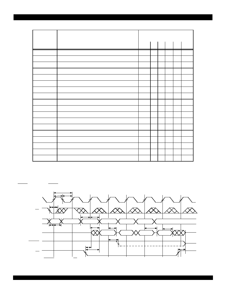
Control Interface Commands
Control Interface Commands
Control Interface Commands
Control Interface Commands
Control Interface Timing Waveform
Control Interface Timing Waveform
Control Interface Timing Waveform
Control Interface Timing Waveform
CTLEN is Low and the CTLEN bit of the configuration register (Bit 31) is LOW for this waveform.
1
All output signals except CRCERR are controlled by OE.
2
The 13-bit cell address, 4-bit selected Switching Memory address, and the 5-bit Edit Buffer Protect and Clear control bits are valid at this time.
COMMAND Bus Bit (CMD5:0)
MSb LSb
Command
1
1.
CMD bus commands not defined in this table are undefined and not to be implemented.
Command Description
5
4
3
2
1
0
GPIx
Get Pre/Post Pend Data from ISAMx
2
2.
"x" represents the specific ISAM or OSAM being accessed (IP0-IP7 or OP0-OP7 respectively).
0
0
0
n
3
3.
"n" represents the appropriate bit of the binary representation of the ISAM or OSAM being accessed (000 to 111).
n
3
n
3
GHIx
Get Header from ISAMx
2
0
0
1
n
3
n
3
n
3
GPE
Get Pre/Post Pend Data from Edit Buffer
0
1
0
0
0
0
GHE
Get Header from Edit Buffer
0
1
0
1
0
0
GST
Get ISAM and OSAM Status Register Bits
0
1
0
0
1
0
GER
Get Error Register Bits
0
1
0
1
1
0
STEx
Store Cell in ISAMx
2
and Input Edit Buffer in Memory
1
0
0
n
3
n
3
n
3
STIx
Store Cell in ISAMx
2
in Memory
1
0
1
n
3
n
3
n
3
LDOx
Load Cell from Memory into OSAMx
2
1
1
0
n
3
n
3
n
3
PPE
Put new Pre/Post Pend in Input Edit Buffer
1
1
1
0
0
0
PHE
Put new Header in Input Edit Buffer
1
1
1
1
0
0
PHEC
Put new Header and new CRC byte in Input Edit Buffer
1
1
1
1
0
1
REF
Refresh Memory
0
1
0
1
1
1
LDC
Load Configuration Register
1
1
1
0
1
0
OPE
Put Pre/Post Pend Data in Output Edit Register
1
1
1
0
1
1
OHE
Put new Header in Output Edit Register
1
1
1
1
1
0
OHEC
Put new Header and new CRC byte in Output Edit Register
1
1
1
0
0
1
NOP
No Operation
1
1
1
1
1
1
PUT
HEADER
STORE
ISAM
GET
HEADER
GET
STATUS
SCLK
CRCERR
3606 drw 07
OE
CS
CMD0-5
IOD0-31
Output -
Old Header
Output -
Status
[ CRC ERROR = LOW ]
GET
STATUS
Input -
New Header
[ AVAILABLE FOR NEXT COMMAND ]
Input -
Cell Addr
t
CYC
t
CH
t
CL
t
SC
t
HC
t
SCM
t
HCM
t
SCM
t
HCM
t
CDIO
t
CDIO
t
DCIO
t
DCIO
t
CDCR
t
OLZ
t
OE
NOP
1
2
t
OHZ

14 of 26
March 31, 2001
IDT77V400
Control Enable Timing Waveform
Control Enable Timing Waveform
Control Enable Timing Waveform
Control Enable Timing Waveform
The CTLEN bit of the configuration register (Bit 31) is LOW for this waveform. If the CTLEN bit of the configuration register is set HIGH at device
initialization the IOD bus will always be in input mode for multiple Switching Memory configurations.
Reset Waveform
Reset Waveform
Reset Waveform
Reset Waveform
Reset function can also be accomplished by holding the RESET bit [Bit 30] High on the IOD bus during a LDC (Load Configuration Register)
command.
1
t
RST
must be greater than two SCLK cycles. Any glitch could cause an erroneous reset operation.
2
RESET must be Low 10ns prior to the next rising SCLK edge to insure that the Reset function is not repeated
Input Port Timing Waveform
Input Port Timing Waveform
Input Port Timing Waveform
Input Port Timing Waveform
1ICLK frequency must not exceed the SCLK frequency.
2
t
SIF
and t
HIF
(I
FRM
Setup and Hold) must be met for each I
CLK
rising edge for I
FRM
Low and High.
Output Port Timing Waveform
Output Port Timing Waveform
Output Port Timing Waveform
Output Port Timing Waveform
1
OFRMx is actually tri-stated by the device one cycle before the end of the frame; the logic Low level is due to the recommended 5k ohm resistor on the OFRMx line.
3606 drw 08
CTLEN
OE
IOD0-31
t
CTEN
t
CTHZ
t
CTLZ
ENABLED
SCLK
t
CYC
2
t
RST
t
RSTL
RESET
3606 drw 09
1
ICLKx
IFRMx
IPxD0-3
Nibble 0
Cell n
Cell n+1
3606 drw 10
Nibble 1
Nibble n
(Last of cell)
t
CYCI
t
CHI
t
CLI
t
SIF
t
HIF
t
SID
t
HID
Nibble 0
2
1
Nibble n
(Last of cell)
OCLKx
OFRMx
OPxD0-3
Nibble 0
Cell n
3606 drw 11
OE
Nibble 0
t
CYCO
t
CHO
t
CLO
t
CDOD
t
DCOD
t
OE
t
CDOF
t
DCOF
t
OHZ
t
OLZ
Cell n+1
1
Nibble n-1
Nibble n-2
1

15 of 26
March 31, 2001
IDT77V400
Input Ports
Input Ports
Input Ports
Input Ports
A 155Mbps input Data Path Interface (DPI) consists of six pins ≠ four
data bits (IPxD0-3), an input clock (ICLKx), and an input framing signal
(IFRMx). A further definition of the DPI interface is available in Technical
Note 34, available on the IDT Web Site (www.idt.com). The "x" in the
signal name corresponds to a port number (0 through 7 for the 8 x 8 port
configuration). IPxD0-3 and IFRMx are synchronous inputs with respect
to the rising edge of ICLKx, and the ICLK frequency must not exceed the
SCLK frequency. Each Input SAM (ISAMx) is double buffered, with each
ISAM buffer able to store a single ATM cell of up to 56 bytes in length.
The 32-bit Header and up to 32 bits of Pre-Pend and/or Post-Pend bytes
may be accessed and modified via the Control Data Bus interface.
The Input Port Timing Waveform assumes that the Switching
Memory has been initialized and the ISAMs are empty. An active HIGH
IFRMx signal indicates that the first nibble of a new cell will be received
on the next rising edge of ICLKx and the cell counter is initialized. Data
will be sequentially clocked into the ISAM buffer on each subsequent
ICLKx rising edge after IFRMx goes LOW. The status register bit indi-
cating ISAMx buffer is full will be set HIGH when the ISAM counter
reaches the stop address. The ISAM start and stop address is
programmed via the configuration register at initialization to establish the
input cell length and protocol. If IFRMx input goes HIGH before the stop
position address is reached, the start byte position address will be
reloaded, the ISAM Full Status indicator will not be set, a Short Cell error
status indicator will be set in the error register, and the cells will be over-
written. If the IFRMx does not go HIGH when the stop position address
is reached, the ISAM Full status indicator and a Long Cell error status
indicator will be set. A Long Cell error results in the beginning portion of
the long cell being kept, the last portion being discarded, and the next
cell being accepted in the other half of the ISAM on the next IFRMx
HIGH. When the IFRMx input stays HIGH, the load start byte position
address process will repeat for every ICLKx and the actual count will not
start until IFRMx goes LOW. A subsequent cell may be input back-to-
back (no dead cycle on the IOD bus). In this case the IFRMx of the
second cell will occur on the same ICLKx rising edge as the last data
nibble of the first cell.
When the control logic returns 32-bits of information across the IOD
bus during a STORE command, the five most significant bits provide the
Byte Edit control for the first word of the input edit buffer. These four
bytes are either cleared, protected, or unaffected depending on the
value of the bits IOD27-31. These five bits are updated each time a
STORE command is executed. IOD31 determines if the function is clear
or protect; IOD 27-30 select which bytes in the first word of the Input edit
buffer are affected. The Edit Buffer Protect/Clear Codes table defines
the possible combination of these bits.
Each of the eight 4-bit input ports is capable of receiving 155Mbps
data; however, the ports can be combined in groups of four bits to
receive data rates up to 1.2Gbps. For example, four 4-bit ports can be
combined to receive 622Mbps traffic. The output ports can also be
combined, via the configuration register, independent of the input data
ports. This allows the Switching Memory to be configured as a concen-
trator, expander, or cell buffer with multiple bus widths. When combining
ports, the chip is internally reconfigured to accept a single master ICLK
for the grouped ports (always using the least significant ICLK/IFRM of
those combined), and the data path is internally switched to correctly
align the ports for CRC generation and Header/Pre-Post Pend compar-
ison. See the Port Configuration Code Table for option definitions. By
varying the input and output port options, one hundred different port
configurations are available to the user to optimize design flexibility.
Output Ports
Output Ports
Output Ports
Output Ports
The output data ports are similar in operation to the input data ports.
There are eight 155Mbps DPI ports, six pins each. Data is transmitted
out the 4-bit data bus (OPxD0-3), synchronous with the output clock
(OCLKx). An output framing signal (OFRMx) is provided which is also
synchronous with respect to OCLKx.
The output port protocol was designed to interface directly with the
input port of another Switching Memory without requiring additional
logic. This allows cascading of multiple Switching Memory chips to
implement wider multiplexers or larger capacity cell buffers without addi-
tional logic. To facilitate cascading, OFRMx has been implemented as a
tri-statable I/O, while OPxD pins are tri-statable outputs. All chip outputs
can be disabled to a high impedance state by asserting the OE pin
HIGH.
Output ports of a single device or of multiple devices may share an
output bus if they are configured in the cell bus mode, where control
logic performs the arbitration between IDT77V400s, or are externally
controlled via the OE. In the cell bus mode configuration, one external
controller would typically drive the control interface of multiple Switching
Memory chips and use the OFRMx to arbitrate the shared bus.
Output SAM (OSAMx) control logic must receive a LDx (Load
OSAMx) instruction from the external controller via the Command Bus to
dispatch a cell. The LDx instruction initiates a cell transfer from the
memory location specified on the IOD Bus to the specified OSAMx. At
this point the user has the option of modifying the Header and the Pre-
Post Pend bytes. When the output buffer has a cell loaded to send,
Switching Memory will immediately assert the specific OFRMx HIGH for
one OCLKx cycle prior to transmitting data. When the OFRMx is then
asserted LOW, the first data nibble of the new cell will appear prior to the
next rising edge of OCLKx. The output port will continue to assert
OFRMx LOW (while the cell is output from OSAMx) for a minimum of
two cycles before the end of the cell transmission. At that time (if in cell
bus mode) OFRMx is released to a high-impedance state during the
cycle before the end of the frame to allow collision free control transfer to
another Switching Memory. After asserting OFRMx HIGH, the OSAMx
EMPTY bit in the status register will be set, indicating that an OSAM
buffer is available for a new cell to be loaded from the memory. The
EMPTY bit is reset when a LDx command is performed and after the cell
is transmitted. It is recommended that a pull down resistor be used on
OFRMx pin to eliminate the possibility of an invalid OFRMx HIGH. The
value of this pull down resistor will be determined by a specific board
design or noise issues. A 5K
resistor is recommended for this pull
down function, although 50-100K
may be sufficient in most applica-
tions.
16 of 26
March 31, 2001
IDT77V400
The OFRM pin is always monitored internally by the Switching Memory. The OFRMx output is released to a High-impedance state when it is in cell
bus mode and a cell is not ready for dispatch. Upon receiving a HIGH OFRMx input, the Switching Memory will hold if a transmission was beginning.
When an output port asserts OFRMx HIGH all of Switching Memories on the bus, including the transmitting Switching Memory, reset the internal start
of frame count. The transmitting IDT77V400 then places the data on the output bus and all Switching Memories on the bus count to the end of the
frame. If OFRMx is an output, the internal OSAMx counter is set to the starting address. The counter will count up to the stop address for each subse-
quent OCLKx rising edge after OFRMx goes low. In this manner, all devices sharing the output bus must be set to the same nibble count. if a switching
memory receives a ldx command while any port is transmitting on the output bus, it will continue counting and wait for the stop address to be reached
before asserting ofrmx and dispatching a cell. this will avoid collisions on the bus; however, it is the responsibility of the external controller to issue only
one ldx command for a shared cell bus within a single cell transmit time.
Functional Waveforms
Functional Waveforms
Functional Waveforms
Functional Waveforms
Figure 6 Functional Waveform - Store Instruction Sequence
1
The Memory Store Cycle requires four cycles to write the cell from the ISAM to the Buffer Memory.
2
The PPE or PHEC commands can be executed at this point in the sequence instead of the PHE command. The IOD bus would then reflect the appropriate bytes in the cell based on
the command used.
3
The 13-bit cell address, 4-bit selected Switching Memory address, and 5-bit Edit Buffer Protect and Clear control bits are valid at this time.
4
STORE ISAM command can only be valid for one cycle during a Memory Store Cycle. Issuing more than one STORE ISAM will cause Buffer Memory write failure.
Figure 7 Functional Waveform - Load Instruction Sequence
1
The Memory Load Cycle requires four cycles to write the cell from the Buffer Memory to the OSAM.
2
The OPE or OHEC commands can be executed at this point in the sequence instead of the OHE command. The IOD bus would then reflect the appropriate cell bytes based on the
command used.
3
The 13-bit cell address and 4-bit selected Switching Memory address are valid at this time
4
LOAD OSAM command can only be valid for one cycle during a Load Sequence. Issuing more than one LOAD OSAM will cause Buffer Memory read failure.
GET HEADER
ISAM
STORE
ISAM
CS
SCLK
IOD0-31
3606 drw 12
CMD0-5
GET
STATUS
Old
Header
Cell
Address
New
Header
Port
Status
Input
Output
MEMORY STORE SEQUENCE
MEMORY STORE CYCLE
IOD BUS
MODE
Output
Input
Input
Input
Input
Input
PUT
HEADER
2
2
1
3
4
GET
HEADER
LOAD
OSAM
CS
SCLK
IOD0-31
3606 drw 13
CMD0-5
GET
STATUS
OR
HEADER
Cell
Address
Header
Data
Port
Status
Input
Output
LOAD SEQUENCE
LOAD CYCLE
IOD BUS
MODE
Input
Input
Output
Input
Input
Input
2
2
1
3
4
Old
Header

17 of 26
March 31, 2001
IDT77V400
Figure 8 Functional Waveform - Refresh Sequence
1
The Refresh sequence begins with the REF command and ends when the four cycle Buffer Memory Refresh has completed.
2
REFRESH command can only be valid for one cycle during a Refresh Sequence. Refresh must be completed prior to another command to avoid data corruption.
Figure 9 Multi-Sequence Functional Waveform Example - Idle, Memory Store, Initiate Memory Store
1
1
CS is Low
2
The 13-bit cell address and 4-bit selected Switching Memory address and 5-bits Edit Buffer Protect and Clear control bits are valid at this time.
Figure 10 Multi-Sequence Functional Waveform Example - Idle, Load, Initiate Load
1
1
CS is Low.
2
The 13-bit cell address and 4-bit selected Switching Memory address are valid at this time.
REFRESH
CS
SCLK
IOD0-31
3606 drw 14
CMD0-5
GET
STATUS
Port
Status
Input
Input
REFRESH SEQUENCE
REFRESH CYCLE
IOD BUS
MODE
Input
Output
Output
Input
Input
Input
Port
Status
GET
STATUS
2
1
SCLK
IOD0-31
CMD0-5
Cell
Address
New
Header
Port
Status
Input
MEMORY STORE SEQUENCE n
MEMORY STORE CYCLE
IOD BUS
MODE
3606 drw 15
GET
STATUS
GET
STATUS
GET HEADER
ISAM
STORE
ISAM
PUT HEADER
GET
STATUS
GET
STATUS
GET
STATUS
GET HEADER
ISAM
STORE
ISAM
Port
Status
Old
Header
Port
Status
Port
Status
Old
Header
Port
Status
Output
Output
Output
Input
Output
Output
Output
Output
MEMORY
STORE SEQUENCE n+1
2
LOAD
OSAM
SCLK
IOD0-31
CMD0-5
Cell
Address
Header
Data
Port
Status
Input
LOAD SEQUENCE n
LOAD CYCLE
IOD BUS
MODE
3606 drw 16
GET
STATUS
GET
STATUS
LOAD
OSAM
OR HEADER
GET
STATUS
GET
STATUS
OR HEADER
Port
Status
Port
Status
Cell
Address
Header
Data
Port
Status
Output
Output
Output
Input
Output
Output
GET
STATUS
Input
Input
Port
Status
LOAD SEQUENCE n+1
2
2
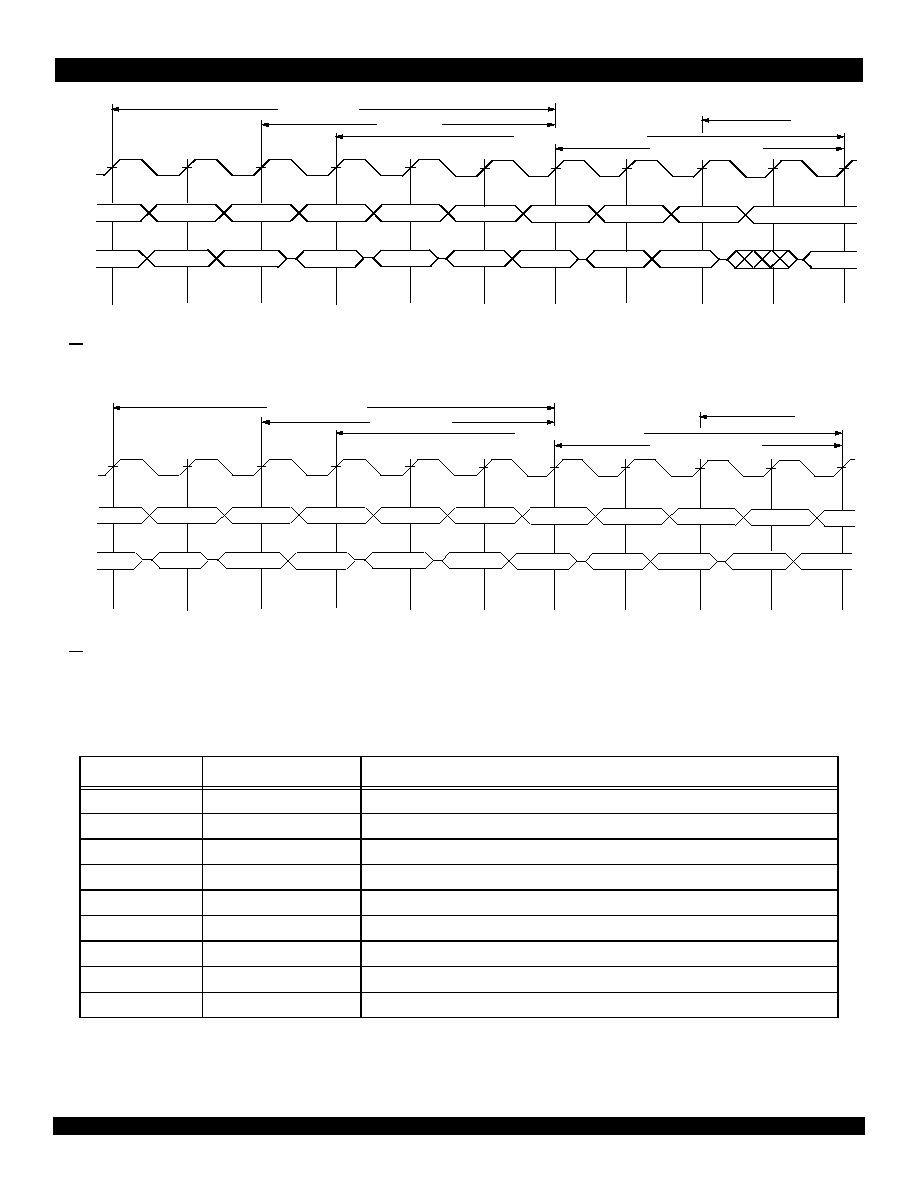
18 of 26
March 31, 2001
IDT77V400
Figure 11 Multi-Sequence Functional Waveform Example - Load, Memory Store, Initiate Refresh
1
1
CS is Low.
2
The 13-bit cell address and 4-bit selected Switching Memory address and 5-bits Edit Buffer Protect and Clear control bits are valid at this time.
Figure 12 Multi - Sequence Functional Waveform Example - Refresh, Memory Store, Initiate Load
1
1
CS is Low.
2
The 13-bit cell address and 4-bit selected Switching Memory address and 5-bit Edit Buffer Protect and Clear control bits are valid at this time.
3
The 13-bit cell address and 4-bit selected Switching Memory address are valid at this time; Clear control bits are ignored during the Load sequence.
Configuration Register Definition
Configuration Register Definition
Configuration Register Definition
Configuration Register Definition
Register Bits
1
1.
Configuration Register Bit number corresponds to the same bit position on the IOD bus. Bit 0 is the LSb bit; bit 31 is the MSb.
Field Name
Field Description
0-3
ISAM Configuration
Four bit configuration code for the input ports as defined in the Table of configuration codes.
4-7
OSAM Configuration
Four bit configuration code for the output ports as defined in the Table of configuration codes.
8-10
ISAM Start
Three bit starting byte position for the ISAMs.
11-16
ISAM Stop
Six bit stop byte position for the ISAMs.
17-19
OSAM Start
Three starting byte position for the OSAMs.
20-25
OSAM Stop
Six bit stop byte position for the OSAMs.
26-29
Chip Address
Four bit field for multiple device configurations.
30
Reset
2
2.
This bit is not stored in the Configuration Register. It must be asserted on the IOD bus to generate asynchronous reset operation.
One bit used to reset the status and output waiting bits.
31
CTLEN
One bit used for the Control Interface outputs during parallel operation.
SCLK
IOD0-31
CMD0-5
Old
Header
Header
Data
New
Header
Output
Input
IOD BUS
MODE
3606 drw 17
GET
STATUS
PUT HEADER
GET
STATUS
REFRESH
Port
Status
Port
Status
Output
Input
Output
Output
Input
Port
Status
STORE
ISAM
LOAD
OSAM
Input
Input
Output
OR HEADER
GET ISAM HEADER
GET
STATUS
GET
STATUS
Cell
Address
Cell
Address
Port
Status
MEMORY STORE SEQUENCE
MEMORY STORE CYCLE
LOAD SEQUENCE
LOAD CYCLE
REFRESH
SEQUENCE
2
SCLK
IOD0-31
CMD0-5
Old
Header
Port
Status
New
Header
Output
Input
MEMORY STORE SEQUENCE
MEMORY STORE CYCLE
REFRESH SEQUENCE
REFRESH CYCLE
IOD BUS
MODE
3606 drw 18
GET
STATUS
PUT HEADER
GET
STATUS
LOAD
OSAM
Port
Status
Port
Status
Output
Input
Input
Output
Input
Port
Status
STORE
ISAM
REFRESH
Output
Input
Output
GET ISAM HEADER
GET
STATUS
Cell
Address
Header
Data
GET
STATUS
OR HEADER
Cell
Address
LOAD
SEQUENCE
2
3

19 of 26
March 31, 2001
IDT77V400
Port Configuration Codes
Port Configuration Codes
Port Configuration Codes
Port Configuration Codes
Config
Code
1,2
1.
Configuration codes are used to initially configure the IDT77V400. These codes are applicable to both the input and output ports, and do not have to be configured the same for
both input and output ports.
2.
The Data Path Interface (DPI) used by the input and output ports provides the option to combine the four bit data widths together to achieve a higher bandwidth port. The entries
in the table are expressed in bus width, and represent the following maximum data rates per port based on ICLK or OCLK frequency:
∑ 4 bit: 155Mbps
∑ 8 bit: 311Mbps
∑ 16 bit: 622Mbps
∑ 32 bit: 1.24Gbps
When four bit busses are combined to obtain a higher bandwidth port, the specific CLK and FRM pin to be used for the new wider port is specified. If not specified the CLK and FRM
pins match the port number. It is suggested that unused ICLK and IFRM pins be pulled up to Vcc through a resistor, and that unused OCLK and OFRM pins be pulled down to Vss
through a resistor. The resistor value is not critical; 5K ohm or less is recommended.
Port Configuration
MSb LSb
0
1
2
3
4
5
6
7
0000
4 bit
4 bit
4 bit
4 bit
4 bit
4 bit
4 bit
4 bit
0001
8 bit, CLK/FRM 0
4 bit
4 bit
4 bit
4 bit
4 bit
4 bit
0010
3
3.
This configuration is not supported by the IDT77V500 Switch Controller. Please use the alternate port assignment option immediately prior to this one in the Port Configuration
Codes table.
4 bit
4 bit
4 bit
4 bit
4 bit
4 bit
8 bit, CLK/FRM 6
0011
8 bit, CLK/FRM 0
8 bit, CLK/FRM 2
4 bit
4 bit
4 bit
4 bit
0100
3
4 bit
4 bit
4 bit
4 bit
8 bit, CLK/FRM 4
8 bit, CLK/FRM 6
0101
8 bit, CLK/FRM 0
8 bit, CLK/FRM 2
8 bit, CLK/FRM 4
4 bit
4 bit
0110
3
4 bit
4 bit
8 bit, CLK/FRM 2
8 bit, CLK/FRM 4
8 bit, CLK/FRM 6
0111
8 bit, CLK/FRM 0
8 bit, CLK/FRM 2
8 bit, CLK/FRM 4
8 bit, CLK/FRM 6
1000
3
4 bit
4 bit
4 bit
4 bit
16 bit, CKL/FRM 4
1001
16 bit, CLK/FRM 0
4 bit
4 bit
4 bit
4 bit
1010
3
4 bit
4 bit
8 bit, CKL/FRM 2
16 bit, CLK/FRM 4
1011
16 bit, CLK/FRM 0
8 bit, CLK/FRM 4
4 bit
4 bit
110
3
8 bit, CLK/FRM 0
8 bit, CLK/FRM 2
16 bit, CLK/FRM 4
1101
16 bit, CLK/FRM 0
8 bit, CLK/FRM 4
8 bit, CLK FRM 6
1110
16 bit, CLK/FRM 0
16 bit, CLK/FRM 4
1111
32 bit, CLK/FRM 0

20 of 26
March 31, 2001
IDT77V400
Status Register Definition
Status Register Definition
Status Register Definition
Status Register Definition
Register
Bit
Port
ISAM
Full
1
1.
Logic 1 (HIGH) indicates the ISAM is full.
ISAM
Error
2
2.
Logic 1 (HIGH) indicates an ISAM error. Error register should be accessed to identify
type of error.
OSAM
Empty
3
3.
Logic 1 (HIGH) indicates the OSAM is empty
CRC
Error
4
4.
Logic 1 (HIGH) indicates CRC error on the ISAM.
IOD0
0
X
--
--
--
IOD1
0
--
X
--
--
IOD2
1
X
--
--
--
IOD3
1
--
X
--
--
IOD4
2
X
--
--
--
IOD5
2
--
X
--
--
IOD6
3
X
--
--
--
IOD7
3
--
X
--
--
IOD8
4
X
--
--
--
IOD9
4
--
X
--
--
IOD10
5
X
--
--
--
IOD11
5
--
X
--
--
IOD12
6
X
--
--
--
IOD13
6
--
X
--
--
IOD14
7
X
--
--
--
IOD15
7
--
X
--
--
IOD16
0
--
--
X
--
IOD17
1
--
--
X
--
IOD18
2
--
--
X
--
IOD19
3
--
--
X
--
IOD20
4
--
--
X
--
IOD21
5
--
--
X
--
IOD22
6
--
--
X
--
IOD23
7
--
--
X
--
IOD24
0
--
--
--
X
IOD25
1
--
--
--
X
IOD26
2
--
--
--
X
IOD27
3
--
--
--
X
IOD28
4
--
--
--
X
IOD29
5
--
--
--
X
IOD30
6
--
--
--
X
IOD31
7
--
--
--
X
Error Register Definition
Error Register Definition
Error Register Definition
Error Register Definition
RAM Address Definition
RAM Address Definition
RAM Address Definition
RAM Address Definition
Used for Store Commands (STEx, STIx) and Load Command
(LDOx).
Register
Bit
Port ISAM Short
Cell Error
1
1.
When the Register Bit is a logic 1(High), the type of error is indicated by an "X".
ISAM Long
Cell Error
1
ISAM
Overflow
1
IOD0
0
X
--
--
IOD1
0
--
X
--
IOD2
1
--
--
X
IOD3
1
X
--
--
IOD4
2
--
X
--
IOD5
2
--
--
X
IOD6
0
X
--
--
IOD7
0
--
X
--
IOD8
0
--
--
X
IOD9
0
X
--
--
IOD10
0
--
X
--
IOD11
0
--
--
X
IOD12
1
X
--
--
IOD13
1
--
X
--
IOD14
2
--
--
X
IOD15
2
X
--
--
IOD16
0
--
X
--
IOD17
0
--
--
X
IOD18
0
X
--
--
IOD19
0
--
X
--
IOD20
0
--
--
X
IOD21
0
X
--
--
IOD22
1
--
X
--
IOD23
1
--
--
X
IOD2431
2
--
--
--
IOD Bit
Description
0-12
Cell address in Buffer Memory
13-16
Switching Memory ID address
(in multiple 77V400 device configurations)
17-26
Unused
27-31
Edit Buffer Protect/Clear Control Bits
1
1.
Updated during STEx and STIx operation.

21 of 26
March 31, 2001
IDT77V400
Edit Buffer Protect/Clear Codes
Edit Buffer Protect/Clear Codes
Edit Buffer Protect/Clear Codes
Edit Buffer Protect/Clear Codes
IOD Bit
1
Description
31
Mode
30
Byte 0
1
1.
Byte 0 represents bits 0-7 of the Input Edit Buffer
Byte 1 represent bits 8-15 of the Input Edit Buffer
Byte 2 represent bits 16-23 of the Input Edit Buffer
Byte 3 represent bits 24-31 of the Input Edit Buffer
Bit 31 is the MSb of the Input Edit Buffer
29
Byte 1
1
28
Byte 2
1
27
Byte 3
1
0
0
0
0
0
No Bytes Selected - No Bytes Cleared
0
0
0
0
1
Clear Byte 3
0
0
0
1
0
Clear Byte 2
0
0
0
1
1
Clear Bytes 2 and 3
0
0
1
0
0
Clear Byte 1
0
0
1
0
1
Clear Bytes 1 and 3
0
0
1
1
0
Clear Bytes 1 and 2
0
0
1
1
1
Clear Bytes 1, 2 and 3
0
1
0
0
0
Clear Byte 0
0
1
0
0
1
Clear Bytes 0 and 3
0
1
0
1
1
Clear Bytes 0 and 2
0
1
0
1
1
Clear Bytes 0, 2 and 3
0
1
1
0
0
Clear Bytes 0 and 1
0
1
1
0
1
Clear Bytes 0, 1 and 3
0
1
1
1
0
Clear Bytes 0, 1 and 2
0
1
1
1
1
Clear Bytes 0, 1, 2 and 3
1
0
0
0
0
No Bytes Selected - No Protection Done
1
0
0
0
1
Protect Byte 3
1
0
0
1
0
Protect Byte 2
1
0
0
1
1
Protect Byte 2 and 3
1
0
1
0
0
Protect Byte 1
1
0
1
0
1
Protect Bytes 1 and 3
1
0
1
1
0
Protect Bytes 1 and 2
1
0
1
1
1
Protect Bytes 1, 2 and 3
1
1
0
0
0
Protect Byte 0
1
1
0
0
1
Protect Bytes 0 and 3
1
1
0
1
1
Protect Bytes 0 and 2
1
1
0
1
1
Protect Bytes 0, 2 and 3
1
1
1
0
0
Protect Bytes 0 and 1
1
1
1
0
1
Protect Byes 0, 1 and 3
1
1
1
1
0
Protect Byes 0, 1 and 2
1
1
1
1
1
Protect Bytes 0, 1, 2 and 3

22 of 26
March 31, 2001
IDT77V400
Cell Alignment Options
Cell Alignment Options
Cell Alignment Options
Cell Alignment Options
Memory Refresh Requirements
Memory Refresh Requirements
Memory Refresh Requirements
Memory Refresh Requirements
The Buffer Memory of the IDT77V400 must be refreshed by the Control Logic periodically to guarantee data retention. This table defines the
maximum refresh interval; that is, the REFRESH command (see "Control Interface Command" Table) must be executed at least 2048 times during
each interval. Refresh rate numbers are calculated using a 36MHz SCLK. Refresh is only required for systems which utilize extended cell storage due
to queuing requirements above 155Mbps.
Cell Configuration
Byte Location in Cell
1
1.
Byte locations are decimal values.
Without HEC
With HEC
SAM
Start
SAM
Stop
SAM
Start
SAM Stop
no-skip
SAM Stop
skip
No Pre/Post Pend Data
4
55
4
0
1
1 byte prepended
3
55
3
0
1
1 byte postpended
4
0
4
1
2
2 bytes prepended
2
55
2
0
1
1 byte prepended and 1 byte postpended
3
0
3
1
2
2 bytes postpended
4
1
4
2
3
3 bytes prepended
1
55
1
0
1
2 bytes prepended and 1 byte postpended
2
0
2
1
2
1 byte prepended and 2 bytes prepended
3
1
3
2
3
3 bytes postpended
4
2
4
3
--
4 bytes prepended
0
55
--
--
--
3 bytes prepended and 1 byte postpended
1
0
--
--
--
2 bytes prepended and 2 bytes postpended
2
1
--
--
--
1 byte prepended and 3 bytes postpended
3
2
--
--
--
4 bytes postpended
4
3
--
--
--
Grade
Maximum Refresh
Interval
77V500
1
INIT Command Value
(Decimal)
1.
This information is provided for applications using the IDT77V500 Switch Controller.
77V500
1
INIT Command Value
(Hex)
Commercial
32ms
9
1FF
Industrial
16ms
9
1FF

23 of 26
March 31, 2001
IDT77V400
77V400 Package Drawing -- 208-pin PQFP
77V400 Package Drawing -- 208-pin PQFP
77V400 Package Drawing -- 208-pin PQFP
77V400 Package Drawing -- 208-pin PQFP
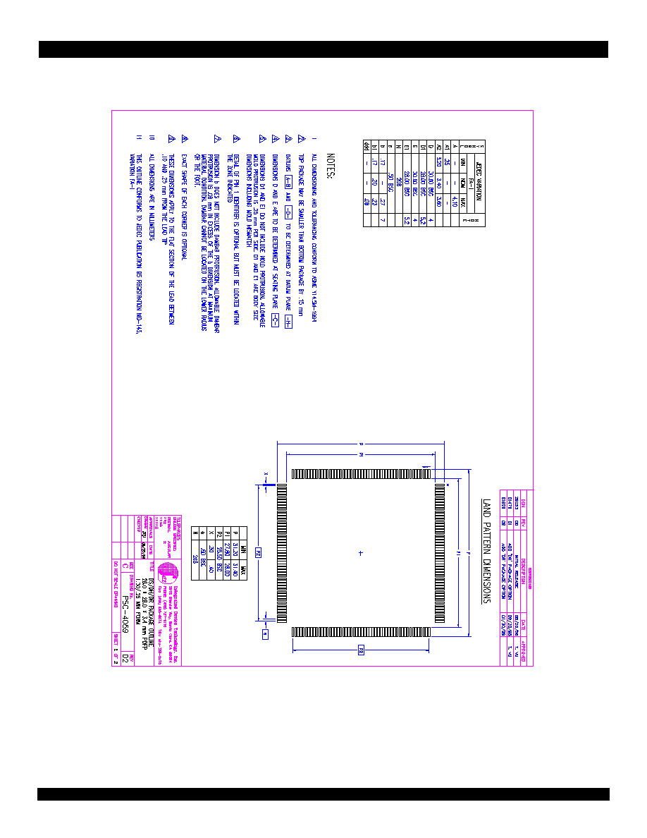
24 of 26
March 31, 2001
IDT77V400
77V400 Package Drawing
77V400 Package Drawing
77V400 Package Drawing
77V400 Package Drawing
--
--
--
--
Page Two
Page Two
Page Two
Page Two

25 of 26
March 31, 2001
IDT77V400
77V400 Package Drawing -- 256-pin BGA
77V400 Package Drawing -- 256-pin BGA
77V400 Package Drawing -- 256-pin BGA
77V400 Package Drawing -- 256-pin BGA
26 of 26
March 31, 2001
IDT77V400
CORPORATE HEADQUARTERS
2975 Stender Way
Santa Clara, CA 95054
for SALES:
800-345-7015
or 408-727-6116
fax:
408-330-1748
www.idt.com
for Tech Support:
switchstarhelp@idt.com
phone:
408-492-8208
SwitchStar and the IDT logo are registered trademarks of Integrated Device Technology, Inc.
Ordering Information
Ordering Information
Ordering Information
Ordering Information
Datasheet Document History
Datasheet Document History
Datasheet Document History
Datasheet Document History
3/1/99:
Updated to new format. Added Industrial Specifications. Added S156 Speed Grade.
Pg. 2 Updated Description to clarify CRC error operation. Block diagram detail updated for clarity.
Pg. 4 Figure 2, Edit Buffer Block Diagram corrected to include Output CRC path.
Pg. 5 Package Diagram notes added for clarification.
Pg. 6 Pin description table descriptions expanded. IP and OP pin number corrections made.
Pg. 7 Pin description table descriptions expanded. V
TERM
in Maximum ratings table reduced to 3.9V. V
IH
Max reduced to V
CC
+0.3V.
Pg. 8 Reset Current parameter removed.
Pg. 14 Pull down resistor values specified in Output Ports section.
Pg. 17 Function Sequence Figures modified to remove first IOD identification (state is really unknown).
Pg. 19 Modified Port Configuration Code Table to clearly identify the subset supported by IDT77V500.
Pg. 20 Improved explanation of Status Register definition and Table; made significant correction and explanation of Error Register definition and Table.
Pg. 22 Recommended Refresh specification added.
Pg. 23 Updated Ordering Information for S156 speed grade and Industrial temperature product.
Pg. 24 Added Preliminary Datasheet definition and Datasheet Document History.
12/11/00:
Moved to final. Updated general format and SwitchStar logo. Changed t
CYCI
, t
CHI
, t
CLI
, t
HOF
, and t
CDOD
specifications. Added ICLK/SCLK relation-
ship condition, see footnote 1. Corrected Note 2 on Input Port Timing Waveform. Corrected Figure 7, Functional Waveform. Corrected Figure 10,
Functional Waveform. Corrected Figures 11 and 12, Functional Waveforms. Added Note 3 to Figure 12. Updated Tech Support phone number.
1/30/01:
Added BGA Packaging to pages 1, 2, 5, 7, 8, and 23.
3/31/01:
Deleted S155 speed grade on pages 10, 11, 23. Relaxed tCYCI, tCHI, tCLI specs on page 11. Added Package Drawings for 208 and 256 pin lay-
outs.
A
Power
999
Speed
A
Package
A
Process/
Temperature
Range
Blank
I
Commercial (0
į
C to +70
į
C)
Industrial (-40
į
C to +85
į
C)
DS
BC
208-pin PQFP (DS208-1)
256 ball BGA (BC256-1)
156
S
Standard Power
XXXXX
Device
Type
Switching Memory
77V400
IDT
3606 drw sp 19
4-bit Port Bandwidth in Mbps
and Parameter Set
Commercial & Industrial
,