1
IDT74CBTLV3257
LOW-VOLTAGE QUAD 2:1 MUX/DEMUX BUS SWITCH
INDUSTRIAL TEMPERATURE RANGE
SEPTEMBER 2001
2001 Integrated Device Technology, Inc.
DSC-5744/1
c
IDT74CBTLV3257
INDUSTRIAL TEMPERATURE RANGE
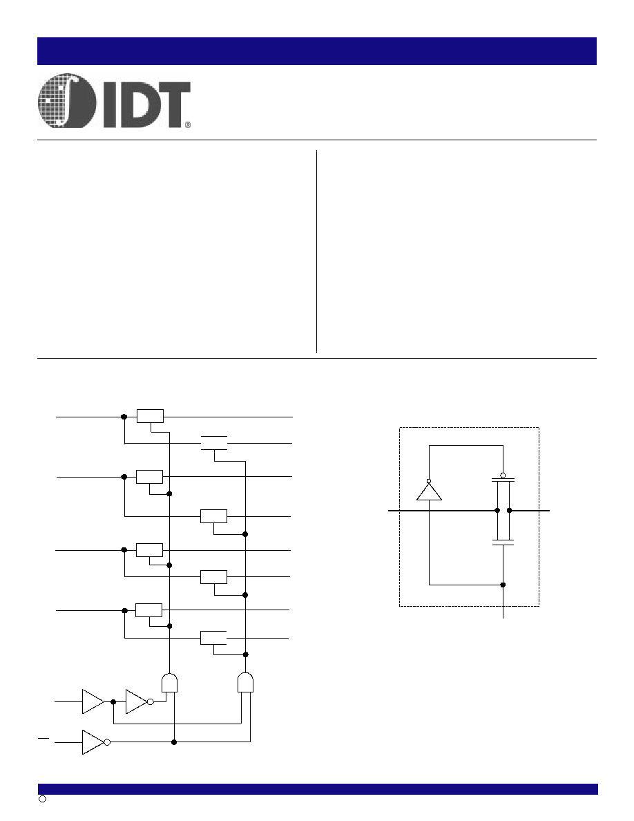
FUNCTIONAL BLOCK DIAGRAM
LOW-VOLTAGE
QUAD 2:1MUX/DEMUX
BUS SWITCH
SIMPLIFIED SCHEMATIC, EACH
SWITCH
FROM ENAB LE
CIRCUITRY
A
B
1A
1B2
2B2
3B2
4A
SW
SW
SW
SW
SW
SW
SW
1B1
2B1
3B1
2A
3A
4B2
4B1
S
OE
SW
DESCRIPTION:
The CBTLV3257 is a quad 2:1 multiplexer/demultiplexer. The low on-
state resistance of the switch allows connections to be made with minimal
propagation delay.
The select (S) input controls the data flow. The multiplexers/demultiplexers
are enabled when the output-enable (
OE) input is low.
To ensure the high-impedance state during power up or power down,
OE should be tied to V
CC
through a pullup resistor; the minimum value of
the resistor is determined by the current-sinking capability of the driver.
FEATURES:
-
Functionally equivalent to QS3257
-
5
Switch Connection between Two Ports
-
Isolation Under Power-Off Conditions
-
Over-voltage tolerant
-
Latch-up performance exceeds 100ma
-
V
CC
= 2.3V - 3.6V, normal range
-
ESD > 2000V per MIL-STD-883, Method 3015;
> 200V using machine model (C = 200pF, R = 0)
-
Available in SSOP, QSOP, and TSSOP packages
APPLICATIONS:
-
3.3V High Speed Bus Switching, Multiplexing, and Bus Isolation
The IDT logo is a registered trademark of Integrated Device Technology, Inc.

2
INDUSTRIAL TEMPERATURE RANGE
IDT74CBTLV3257
LOW-VOLTAGE QUAD 2:1 MUX/DEMUX BUS SWITCH
PIN CONFIGURATION
QSOP/ SSOP/ TSSOP
TOP VIEW
ABSOLUTE MAXIMUM RATINGS
(1)
Symbol
Description
Max.
Unit
V
CC
Supply Voltage Range
≠0.5 to 4.6
V
V
I
Input Voltage Range
≠0.5 to 4.6
V
Continuous Channel Current
128
mA
I
IK
Input Clamp Current, V
I/O
< 0
≠50
mA
T
STG
Storage Temperature
≠65 to +150
∞C
NOTES:
1. Stresses greater than those listed under ABSOLUTE MAXIMUM
RATINGS may cause permanent damage to the device. This is a
stress rating only and functional operation of the device at these or
any other conditions above those indicated in the operational sections
of this specification is not implied. Exposure to absolute maximum
rating conditions for extended periods may affect reliability.
FUNCTION TABLE
(1)
Inputs
OE
S
Function
L
L
A Port = B1 Port
L
H
A Port = B2 Port
H
X
Disconnect
NOTE:
1. H = HIGH Voltage Level
L = LOW Voltage Level
X = Don't Care
V
CC
S
4B1
1B2
4B2
1A
4A
2B1
3B1
2B2
3B2
2A
1B1
OE
GN D
3A
SO16-7
SO16-9
SO16-10
16
1
3
14
4
13
5
12
6
11
7
10
2
15
9
8
OPERATING CHARACTERISTICS, T
A
= 25
∞
C
Symbol
Parameter
Test Conditions
Min.
Max.
Unit
V
CC
Supply Voltage
2.3
3.6
V
V
IH
High-Level Control Input Voltage
V
CC
= 2.3V to 2.7V
1.7
--
V
V
CC
= 2.7V to 3.6V
2
--
V
IL
Low-Level Control Input Voltage
V
CC
= 2.3V to 2.7V
--
0.7
V
V
CC
= 2.7V to 3.6V
--
0.8
T
A
Operating Free-Air Temperature
-
40
+85
∞
C
NOTE:
1. All unused control inputs of the device must be held at V
CC
or GND to ensure proper operation.

3
IDT74CBTLV3257
LOW-VOLTAGE QUAD 2:1 MUX/DEMUX BUS SWITCH
INDUSTRIAL TEMPERATURE RANGE
DC ELECTRICAL CHARACTERISTICS OVER OPERATING RANGE
Following Conditions Apply Unless Otherwise Specified:
Operating Condition: T
A
= ≠ 40∞C to +85∞C
Symbol
Parameter
Test Conditions
Min.
Typ.
(1)
Max.
Unit
V
IK
Control Inputs, Data I/O
V
CC
= 3V, I
I
=
-
18mA
--
--
≠ 1.2
V
I
I
Control Inputs, Data I/O
V
CC
= 3.6V, V
I
= V
CC
or GND
--
--
±1
µ
A
I
OZ
Data I/O
V
CC
= 3.6V, V
O
= 0 or 3.6V, switch disabled
--
--
20
µ
A
I
OFF
V
CC
= 0, V
I
or V
O
= 0 to 3.6V
--
--
50
µ
A
I
CC
V
CC
= 3.6V, I
O
= 0, V
I
= V
CC
or GND
--
--
10
µ
A
I
CC
(2)
Control Inputs
V
CC
= 3.6V, One input at 3V
,
Other inputs at V
CC
or GND
--
--
300
µ
A
C
I
Control Inputs
V
I
= 3V or 0
--
4
--
pF
C
IO(OFF)
A port
V
O
= 3V or 0,
OE = V
CC
= 3.3V
--
13
--
pF
B port
--
6
--
Max at V
CC
= 2.3V
V
I
= 0
I
O
= 64mA
--
5
8
Typ at V
CC
= 2.5V
I
O
= 24ma
--
5
8
R
ON
(3)
V
I
= 1.7V
I
O
= 15mA
--
27
40
V
I
= 0
I
O
= 64mA
--
5
7
V
CC
= 3V
I
O
= 24mA
--
5
7
V
I
= 2.4V
I
O
= 15mA
--
10
15
NOTES:
1. Typical values are at V
CC
= 3.3V, +25∞C ambient.
2. The increase in supply current is attributable to each input that is at the specified voltage level rather than V
CC
or GND.
3. This is measured by the voltage drop between the A and B terminals at the indicated current through the switch. On-state resistance is determined
by the lower of the voltages of the two (A or B) terminals.
SWITCHING CHARACTERISTICS
V
CC
= 2.5V ± 0.2V
V
CC
= 3.3V ± 0.3V
Symbol
Parameter
Min.
Max.
Min.
Max.
Unit
t
PD(1)
Propagation Delay
A to B or B to A
-
0.15
-
0.25
ns
t
SEL
Select Time
S to A or B
1
6.1
1
5.3
ns
t
EN
Enable Time
S to B
1
6.1
1
5.3
ns
t
DIS
Disable Time
S to B
1
4.8
1
4.5
ns
t
EN
Enable Time
OE to A or B
1
5.6
1
5
ns
t
DIS
Disable Time
OE to A or B
1
5.5
1
5.5
ns
NOTE:
1. The propagation delay is the calculated RC time constant of the typical on-state resistance of the switch and the specified load capacitance when
driven by an ideal voltage source (zero output impedance).

4
INDUSTRIAL TEMPERATURE RANGE
IDT74CBTLV3257
LOW-VOLTAGE QUAD 2:1 MUX/DEMUX BUS SWITCH
Open
V
LO AD
GN D
V
C C
Pulse
Generator
D .U .T.
500
500
C
L
R
T
V
IN
V
O U T
(1 , 2)
SAME PHASE
IN PU T TR AN SITIO N
OPPO SITE PHASE
IN PU T TR AN SITIO N
0V
0V
V
OH
V
O L
t
PLH
t
PH L
t
PH L
t
PLH
OU TPU T
V
IH
V
T
V
T
V
IH
V
T
C ON TR OL
IN PU T
t
PLZ
0V
OU TPU T
N OR M A LLY
LOW
t
P Z H
0V
SW ITCH
CLO SE D
OU TPU T
N OR M A LLY
H IGH
ENABLE
D ISA B LE
SW ITCH
O P E N
t
PH Z
0V
V
O L +
V
LZ
V
O H
V
T
V
T
t
PZL
V
LO AD /2
V
LO AD /2
V
IH
V
T
V
O L
V
O H -
V
H Z
TEST CIRCUITS AND WAVEFORMS
PROPAGATION DELAY/ SELECT TIME
TEST CIRCUITS FOR ALL OUTPUTS
ENABLE AND DISABLE TIMES
TEST CONDITIONS
Symbol
V
CC
(1)
= 3.3V ± 0.3V
V
CC
(2)
= 2.5V ± 0.2V
Unit
V
LOAD
6
2 x Vcc
V
V
IH
3
Vcc
V
V
T
1.5
V
CC
/2
V
V
LZ
300
150
mV
V
HZ
300
150
mV
C
L
50
30
pF
SWITCH POSITION
Test
Switch
t
PLZ
/
t
PZL
V
LOAD
t
PHZ/
t
PZH
GND
t
PD
Open
t
SEL
Open
DEFINITIONS:
C
L
= Load capacitance: includes jig and load capacitance.
R
T
= Termination resistance: should be equal to Z
OUT
of the pulse
generator.
NOTES:
1. Pulse Generator for all pulses: Rate
10MHz; t
F
2.5ns, t
R
2.5ns
2. Pulse Generator for all pulses: Rate
10MHz; t
F
2ns, t
R
2ns
NOTE:
1. Diagram shown for Input Control Enable-LOW and Input Control
Disable-HIGH.

5
IDT74CBTLV3257
LOW-VOLTAGE QUAD 2:1 MUX/DEMUX BUS SWITCH
INDUSTRIAL TEMPERATURE RANGE
ORDERING INFORMATION
IDT
XX
CBTLV
XXX
XX
Package
Device Type
Temp. Range
Q
PY
PG
74
Quarter-Size Small Outline Package (SO16-7)
Shrink Small Outline Package (SO16-9)
Thin Shrink Sm all Outline Package (SO16-10)
Low-Voltage Quad 2:1 Mux/Dem ux Bus Switch
≠40∞C to +85∞C
3257
CORPORATE HEADQUARTERS
for SALES:
for Tech Support:
2975 Stender Way
800-345-7015 or 408-727-6116
logichelp@idt.com
Santa Clara, CA 95054
fax: 408-492-8674
(408) 654-6459
www.idt.com