JULY 2004
DSC-3622/06
1
©2004 Integrated Device Technology, Inc.
Features
512K x 8 advanced high-speed CMOS Static RAM
JEDEC Center Power / GND pinout for reduced noise
Equal access and cycle times
-- Commercial and Industrial: 10/12/15ns
Single 3.3V power supply
One Chip Select plus one Output Enable pin
Bidirectional data inputs and outputs directly
TTL-compatible
Low power consumption via chip deselect
Available in 36-pin, 400 mil plastic SOJ package and
44-pin, 400 mil TSOP.
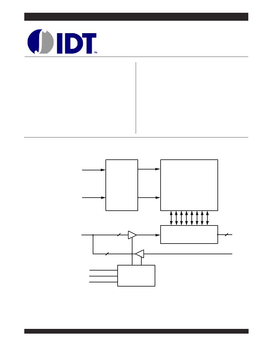
Functional Block Diagram
Description
The IDT71V424 is a 4,194,304-bit high-speed Static RAM organized
as 512K x 8. It is fabricated using IDT's high-perfomance, high-reliability
CMOS technology. This state-of-the-art technology, combined with inno-
vative circuit design techniques, provides a cost-effective solution for high-
speed memory needs.
The IDT71V424 has an output enable pin which operates as fast as
5ns, with address access times as fast as 10ns. All bidirectional inputs and
outputs of the IDT71V424 are TTL-compatible and operation is from a
single 3.3V supply. Fully static asynchronous circuitry is used, requiring
no clocks or refresh for operation.
The IDT71V424 is packaged in a 36-pin, 400 mil Plastic SOJ and 44-
pin, 400 mil TSOP.
ADDRESS
DECODER
4,194,304-BIT
MEMORY ARRAY
I/O CONTROL
∑
∑
∑
A
0
A
18
8
8
I/O
0
- I/O
7
8
CONTROL
LOGIC
WE
OE
CS
3622 drw 01
∑
∑
∑
3.3V CMOS Static RAM
4 Meg (512K x 8-Bit)
IDT71V424S
IDT71V424L
6.42
2
IDT71V424S, IDT71V424L, 3.3V CMOS Static RAM
4 Meg (512K x 8-bit) Commercial and Industrial Temperature Ranges
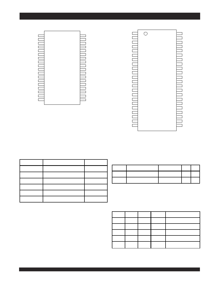
1
2
3
4
5
6
7
8
9
10
11
12
13
14
15
16
17
18
19
20
21
22
A5
NC
NC
A9
A8
A7
WE
I/03
I/02
V
SS
V
DD
I/01
I/00
CS
A2
A1
A0
44
43
42
41
40
39
38
37
36
35
34
33
32
31
30
29
28
27
26
25
24
23
NC
NC
A15
OE
I/07
I/06
V
SS
V
DD
I/05
I/04
A14
A13
A11
A10
NC
NC
NC
NC
A12
SO44-2
3622 drw 11
NC
NC
A3
A4
A6
A16
A17
A18
A0
A1
A2
A3
CS
I/O 0
V
DD
V
SS
I/O 2
WE
A4
A5
A6
A7
1
2
3
4
5
6
7
8
9
10
11
12
13
14
15
16
NC
A18
A17
A16
OE
I/O 7
I/O 6
V
SS
V
DD
I/O 5
A14
A13
A12
A11
36
35
34
33
32
31
30
29
28
27
26
25
24
23
22
21
SO36-1
17
18
19
20
I/O 1
I/O 3
I/O 4
NC
A8
A9
A10
A15
3622 drw 02
SOJ
Top View
Pin Configuration
Truth Table
(1,2)
Capacitance
(T
A
= +25∞C, f = 1.0MHz, SOJ package)
Pin Configuration
TSOP
Top View
A
0
≠ A
18
Address Inputs
Input
CS
Chip Select
Input
WE
Write Enable
Input
OE
Output Enable
Input
I/O
0
- I/O
7
Data Input/Output
I/O
V
DD
3.3V Power
Power
V
SS
Ground
Gnd
3622 tbl 02
Pin Description
Symbol
Parameter
(1)
Conditions
Max.
Unit
C
IN
Input Capacitance
V
IN
= 3dV
7
pF
C
I/O
I/O Capacitance
V
OUT
= 3dV
8
pF
3622 tbl 03
NOTE:
1. This parameter is guaranteed by device characterization, but not production
tested.
CS
OE
WE
I/O
Function
L
L
H
DATA
OUT
Read Data
L
X
L
DATA
IN
Write Data
L
H
H
High-Z
Output Disabled
H
X
X
High-Z
Deselected - Standby (I
SB
)
V
HC
(3)
X
X
High-Z
Deselected - Standby (I
SB1
)
3622 tbl 01
NOTES:
1. H = V
IH
, L = V
IL
, x = Don't care.
2. V
LC
= 0.2V, V
HC
= V
DD
-0.2V.
3. Other inputs
V
HC
or
V
LC
.
6.42
3
IDT71V424S, IDT71V424L, 3.3V CMOS Static RAM
4 Meg (512K x 8-bit) Commercial and Industrial Temperature Ranges
Absolute Maximum Ratings
(1)
Recommended Operating
Temperature and Supply Voltage
Recommended DC Operating
Conditions
DC Electrical Characteristics
(V
DD
= Min. to Max., Commercial and Industrial Temperature Ranges)
DC Electrical Characteristics
(1, 2, 3)
(V
DD
= Min. to Max., V
LC
= 0.2V, V
HC
= V
DD
≠ 0.2V)
NOTE:
1. Stresses greater than those listed under ABSOLUTE MAXIMUM RATINGS may
cause permanent damage to the device. This is a stress rating only and
functional operation of the device at these or any other conditions above those
indicated in the operational sections of this specification is not implied. Exposure
to absolute maximum rating conditions for extended periods may affect
reliability.
NOTES:
1. V
IH
(max.) = V
DD
+2V for pulse width less than 5ns, once per cycle.
2. V
IL
(min.) = ≠2V for pulse width less than 5ns, once per cycle.
NOTES:
1. All values are maximum guaranteed values.
2. All inputs switch between 0.2V (Low) and V
DD
- 0.2V (High).
3. Power specifications are preliminary.
4. f
MAX
= 1/t
RC
(all address inputs are cycling at f
MAX
); f = 0 means no address input lines are changing.
5. Standard power 10ns (S10) speed grade only.
Symbol
Rating
Value
Unit
V
DD
Supply Voltage Relative to
V
SS
-0.5 to +4.6
V
V
IN
, V
OUT
Terminal Voltage Relative
to V
SS
-0.5 to V
DD
+0.5
V
T
BIAS
Temperature Under Bias
-55 to +125
o
C
T
STG
Storage Temperature
-55 to +125
o
C
P
T
Power Dissipation
1
W
I
OUT
DC Output Current
50
mA
3622 tbl 04
Symbol
Parameter
Min.
Typ.
Max.
Unit
V
DD
Supply Voltage
3.0
3.3
3.6
V
V
SS
Ground
0
0
0
V
V
IH
Input High Voltage
2.0
____
V
DD
+0.3
(1)
V
V
IL
Input Low Voltage
-0.3
(2)
____
0.8
V
3622 tbl 06
Grade
Temperature
V
SS
V
DD
Commercial
0∞ C to +70∞ C
0V
See Below
Industrial
≠40∞ C to +85∞ C
0V
See Below
3622 tbl 05
Symbol
Parameter
Test Condition
IDT71V424
Min.
Max. Unit
|I
LI
|
Input Leakage Current
V
DD
= Max., V
IN
= V
SS
to V
DD
___
5
µ A
|I
LO
|
Output Leakage Current
V
DD
= Max.,
CS = V
IH
, V
OUT
= V
SS
to V
DD
___
5
µ A
V
OL
Output Low Voltage
I
OL
= 8mA, V
DD
= Min.
___
0.4
V
V
OH
Output High Voltage
I
OH
= -4mA, V
DD
= Min.
2.4
___
V
3622 tbl 07
Symbol
Parameter
71V424S/L 10
71V424S/L 12
71V424S/L 15
Unit
Com'l.
Ind.
(5)
Com'l.
Ind.
(5)
Com'l.
Ind.
(5)
I
CC
Dynamic Operating Current
CS < V
LC
, Outputs Open, V
DD
= Max., f = f
MAX
(4)
S
180
180
170
170
160
160
mA
L
165
___
155
155
145
145
mA
I
SB
Dynamic Standby Power Supply Current
CS > V
HC
, Outputs Open, V
DD
= Max., f = f
MAX
(4)
S
60
60
55
55
50
50
mA
L
55
___
50
50
45
45
mA
I
SB1
Full Standby Power Supply Current (static)
CS > V
HC
, Outputs Open, V
DD
= Max., f = 0
(4)
S
20
20
20
20
20
20
mA
L
10
___
10
10
10
10
mA
3622 tbl 08
6.42
4
IDT71V424S, IDT71V424L, 3.3V CMOS Static RAM
4 Meg (512K x 8-bit) Commercial and Industrial Temperature Ranges
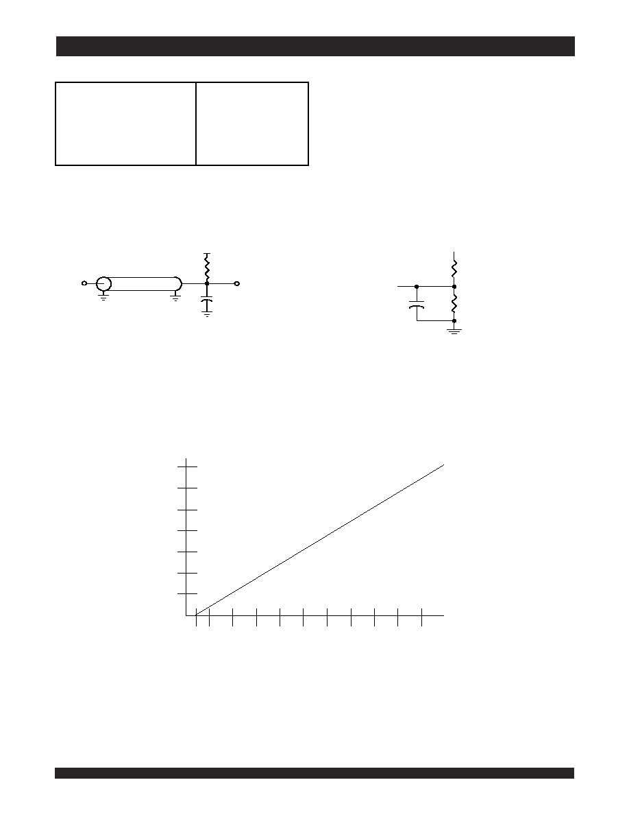
AC Test Loads
AC Test Conditions
Figure 1. AC Test Load
Figure 2. AC Test Load
(for t
CLZ
, t
OLZ
, t
CHZ
, t
OHZ
, t
OW,
and t
WHZ
)
Figure 3. Output Capacitive Derating
*Including jig and scope capacitance.
3622 drw 04
320
350
5pF*
DATA
OUT
3.3V
1
2
3
4
5
6
7
20
40
60 80 100 120 140 160 180 200
t
AA,
t
ACS
(Typical, ns)
CAPACITANCE (pF)
8
3622 drw 05
∑
∑
∑
∑
∑
∑
∑
+1.5V
50
I/O
Z
0
= 50
3622 drw 03
30pF
Input Pulse Levels
Input Rise/Fall Times
Input Timing Reference Levels
Output Reference Levels
AC Test Load
GND to 3.0V
1.5ns
1.5V
1.5V
See Figure 1, 2 and 3
3622 tbl 09
6.42
5
IDT71V424S, IDT71V424L, 3.3V CMOS Static RAM
4 Meg (512K x 8-bit) Commercial and Industrial Temperature Ranges
71V424S/L10
(2)
71V424S/L12
71V424S/L15
Symbol
Parameter
Min.
Max.
Min.
Max.
Min.
Max.
Unit
READ CYCLE
t
RC
Read Cycle Time
10
____
12
____
15
____
ns
t
AA
Address Access Time
____
10
____
12
____
15
ns
t
ACS
Chip Select Access Time
____
10
____
12
____
15
ns
t
CLZ
(1)
Chip Select to Output in Low-Z
4
____
4
____
4
____
ns
t
CHZ
(1)
Chip Deselect to Output in High-Z
____
5
____
6
____
7
ns
t
OE
Output Enable to Output Valid
____
5
____
6
____
7
ns
t
OLZ
(1)
Output Enable to Output in Low-Z
0
____
0
____
0
____
ns
t
OHZ
(1)
Output Disable to Output in High-Z
____
5
____
6
____
7
ns
t
OH
Output Hold from Address Change
4
____
4
____
4
____
ns
t
PU
(1)
Chip Select to Power Up Time
0
____
0
____
0
____
ns
t
PD
(1)
Chip Deselect to Power Down Time
____
10
____
12
____
15
ns
WRITE CYCLE
t
WC
Write Cycle Time
10
____
12
____
15
____
ns
t
AW
Address Valid to End of Write
8
____
8
____
10
____
ns
t
CW
Chip Select to End of Write
8
____
8
____
10
____
ns
t
AS
Address Set-up Time
0
____
0
____
0
____
ns
t
WP
Write Pulse Width
8
____
8
____
10
____
ns
t
WR
Write Recovery Time
0
____
0
____
0
____
ns
t
DW
Data Valid to End of Write
6
____
6
____
7
____
ns
t
DH
Data Hold Time
0
____
0
____
0
____
ns
t
OW
(1)
Output Active from End of Write
3
____
3
____
3
____
ns
t
WHZ
(1)
Write Enable to Output in High-Z
____
6
____
7
____
7
ns
3622 tbl 10
NOTES:
1. This parameter guaranteed with the AC load (Figure 2) by device characterization, but is not production tested.
2. 0∫C to +70∫C temperature range only for low power 10ns (L10) speed grade.
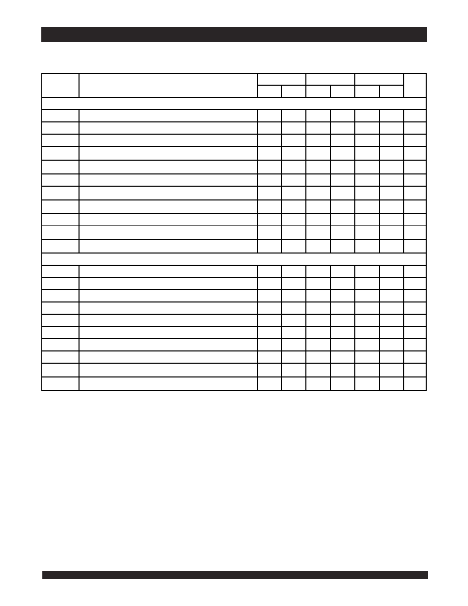
AC Electrical Characteristics
(V
CC
= 3.3V ± 10%, Commercial and Industrial Temperature Ranges)
6.42
6
IDT71V424S, IDT71V424L, 3.3V CMOS Static RAM
4 Meg (512K x 8-bit) Commercial and Industrial Temperature Ranges
Timing Waveform of Read Cycle No. 2
(1, 2, 4)
NOTES:
1.
WE is HIGH for Read Cycle.
2. Device is continuously selected,
CS is LOW.
3. Address must be valid prior to or coincident with the later of
CS transition LOW; otherwise t
AA
is the limiting parameter.
4.
OE is LOW.
5. Transition is measured ±200mV from steady state.
Timing Waveform of Read Cycle No. 1
(1)
ADDRESS
3622 drw 06
OE
CS
DATA
OUT
(5)
(5)
(5)
(5)
DATA
OUT
VALID
HIGH IMPEDANCE
t
AA
t
RC
t
OE
t
ACS
t
OLZ
t
CHZ
t
CLZ
(3)
t
OHZ
V
CC
SUPPLY
CURRENT
t
PU
t
PD
I
CC
I
SB
DATA
OUT
ADDRESS
3622 drw 07
t
RC
t
AA
t
OH
t
OH
DATA
OUT
VALID
PREVIOUS DATA
OUT
VALID
6.42
7
IDT71V424S, IDT71V424L, 3.3V CMOS Static RAM
4 Meg (512K x 8-bit) Commercial and Industrial Temperature Ranges
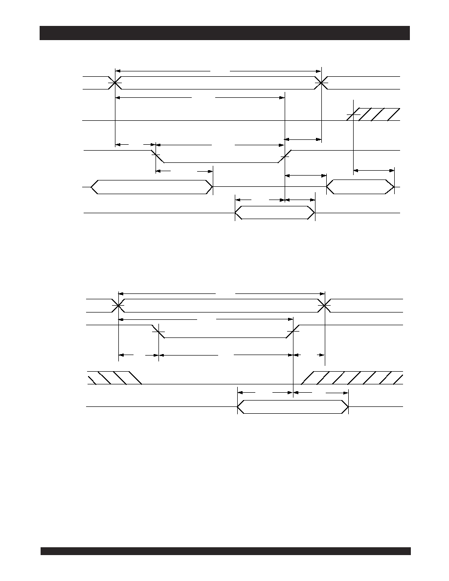
Timing Waveform of Write Cycle No. 1 (WE Controlled Timing)
(1, 2, 4)
Timing Waveform of Write Cycle No. 2 (CS Controlled Timing)
(1, 4)
NOTES:
1. A write occurs during the overlap of a LOW
CS and a LOW WE.
2.
OE is continuously HIGH. During a WE controlled write cycle with OE LOW, t
WP
must be greater than or equal to t
WHZ
+ t
DW
to allow the I/O drivers to turn off and
data to be placed on the bus for the required t
DW
. If
OE is HIGH during a WE controlled write cycle, this requirement does not apply and the minimum write pulse
is the specified t
WP
.
3. During this period, I/O pins are in the output state, and input signals must not be applied.
4. If the
CS LOW transition occurs simultaneously with or after the WE LOW transition, the outputs remain in a high impedance state. CS must be active during the t
CW
write period.
5. Transition is measured ±200mV from steady state.
ADDRESS
CS
WE
DATA
OUT
DATA
IN
3622 drw 08
(5)
(2)
(5)
(5)
DATA
IN
VALID
HIGH IMPEDANCE
t
WC
t
AW
t
AS
t
WHZ
t
WP
t
CHZ
t
OW
t
DW
t
DH
t
WR
(3)
(3)
CS
ADDRESS
DATA
IN
3622 drw 09
t
AW
t
WC
t
CW
t
AS
t
WR
t
DW
t
DH
DATA
IN
VALID
WE
6.42
8
IDT71V424S, IDT71V424L, 3.3V CMOS Static RAM
4 Meg (512K x 8-bit) Commercial and Industrial Temperature Ranges
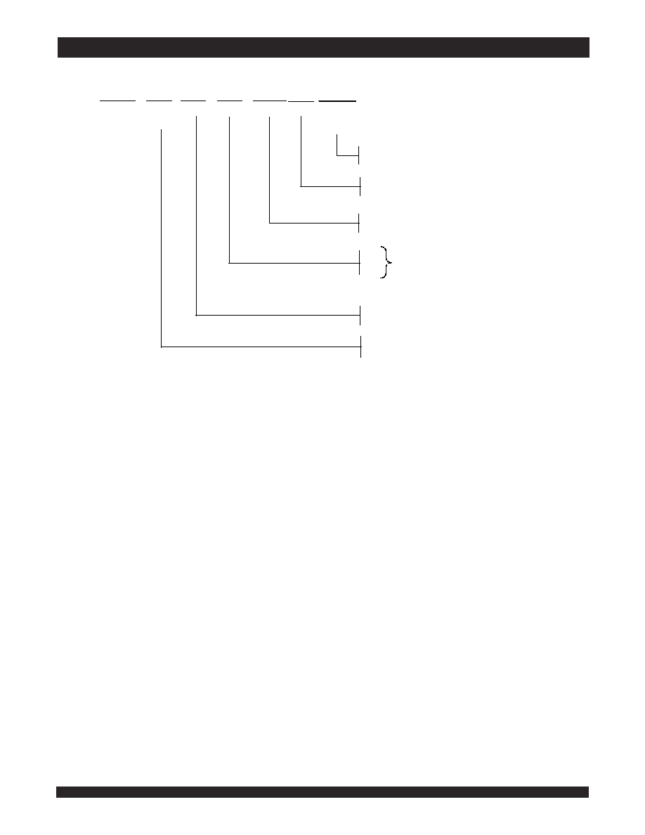
Ordering Information
X
Power
XX
Speed
XXX
Package
X
Process/
Temperature
Range
Blank
I
Commercial (0∞C to +70∞C)
Industrial (≠40∞C to +85∞C)
Y
PH
36-pin 400 mil SOJ (SO36-1)
44-pin TSOP Type II (SO44-2)
10*
12
15
71V424
Device
Type
IDT
Speed in nanoseconds
3622 drw 10
S
L
Standard Power
Low Power
* Commercial only for low power 10ns (L10) speed grade.
X
Die
Revision
Blank
First Generation or current stepping being shipped
X
G
Restricted hazardous substance device

6.42
9
IDT71V424S, IDT71V424L, 3.3V CMOS Static RAM
4 Meg (512K x 8-bit) Commercial and Industrial Temperature Ranges
Datasheet Document History
8/13/99
Updated to new format
Pg. 2
Removed SO44-1 from TSOP pinout
Pg. 7
Revised footnotes on Write Cycle No. 1 diagram
Removed footnote for t
WR
on Write Cycle No. 2 diagram
Pg. 9
Added Datasheet Document History
8/31/99
Pg. 1≠9
Added Industrial temperature range offerings
11/22/02
Pg. 8
Added die revision option to ordering information
07/31/03
Pg. 8
Updated note, L10 speed grade commercial temperature only and updated die stepping from YF to Y.
07/28/04
Pg. 3
Increased ISB for all "L" and S15 speeds by 10mA and increased for S12 speed by 5mA (refer to
PCN# SR-0402-02).
Pg. 8
Added "Restricted hazardous substance device" to the ordering information.
CORPORATE HEADQUARTERS
for SALES:
for Tech Support:
2975 Stender Way
800-345-7015 or 408-727-6116
sramhelp@idt.com
Santa Clara, CA 95054
fax: 408-492-8674
800-544-7726
www.idt.com
The IDT logo is a registered trademark of Integrated Device Technology, Inc.