Integrated Device Technology, Inc.
INDUSTRIAL AND COMMERCIAL TEMPERATURE RANGES
MAY 1997
©
1997 Integrated Device Technology, Inc.
DSC-3101/04
LOW POWER
3.3V CMOS FAST SRAM
256K (32K x 8-BIT)
IDT71V256SA
The IDT logo is a registered trademark of Integrated Device Technology, Inc.
FEATURES
∑ Ideal for high-performance processor secondary cache
∑ Commercial (0
∞
to 70
∞
C) and Industrial (-40
∞
to 85
∞
C)
temperature options
∑ Fast access times:
-- Commercial: 10/12/15/20ns
-- Industrial: 15ns
∑ Low standby current (maximum):
-- 2mA full standby
∑ Small packages for space-efficient layouts:
-- 28-pin 300 mil SOJ
-- 28-pin 300 mil plastic DIP (Commercial only)
-- 28-pin TSOP Type I
∑ Produced with advanced high-performance CMOS
technology
∑ Inputs and outputs are LVTTL-compatible
∑ Single 3.3V(
±
0.3V) power supply
DESCRIPTION
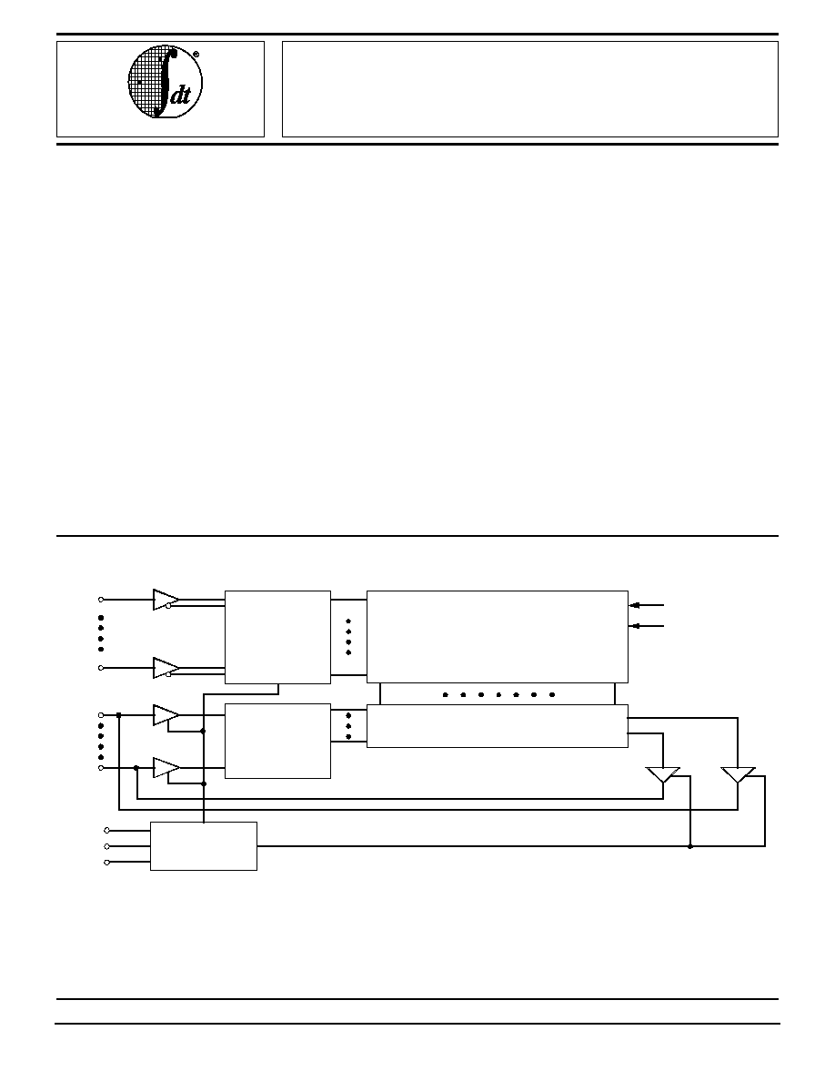
The IDT71V256SA is a 262,144-bit high-speed static RAM
organized as 32K x 8. It is fabricated using IDT's high-
performance, high-reliability CMOS technology.
The IDT71V256SA has outstanding low power character-
istics while at the same time maintaining very high perfor-
mance. Address access times of as fast as10 ns are ideal for
3.3V secondary cache in 3.3V desktop designs.
When power management logic puts the IDT71V256SA in
standby mode, its very low power characteristics contribute to
extended battery life. By taking
CS
HIGH, the SRAM will
automatically go to a low power standby mode and will remain
in standby as long as
CS
remains HIGH. Furthermore, under
full standby mode (
CS
at CMOS level, f=0), power consump-
tion is guaranteed to always be less than 6.6mW and typically
will be much smaller.
The IDT71V256SA is packaged in 28-pin 300 mil SOJ, 28-
pin 300 mil plastic DIP, and 28-pin 300 mil TSOP Type I
packaging.
A
0
ADDRESS
DECODER
262,144 BIT
MEMORY ARRAY
I/O CONTROL
3101 drw 01
INPUT
DATA
CIRCUIT
WE
CS
V
CC
GND
A
14
I/O
0
I/O
7
CONTROL
CIRCUIT
OE
FUNCTIONAL BLOCK DIAGRAM
1
2
IDT71V256SA
3.3V CMOS STATIC RAM 256K (32K x 8-BIT)
INDUSTRIAL AND COMMERCIAL TEMPERATURE RANGES
RECOMMENDED OPERATING
TEMPERATURE AND SUPPLY VOLTAGE
Grade
Temperature
GND
V
CC
Commercial
0
∞
C to +70
∞
C
0V
3.3V
±
0.3V
Industrial
-40
∞
C to +85
∞
C
0V
3.3V
±
0.3V
3101 tbl 05
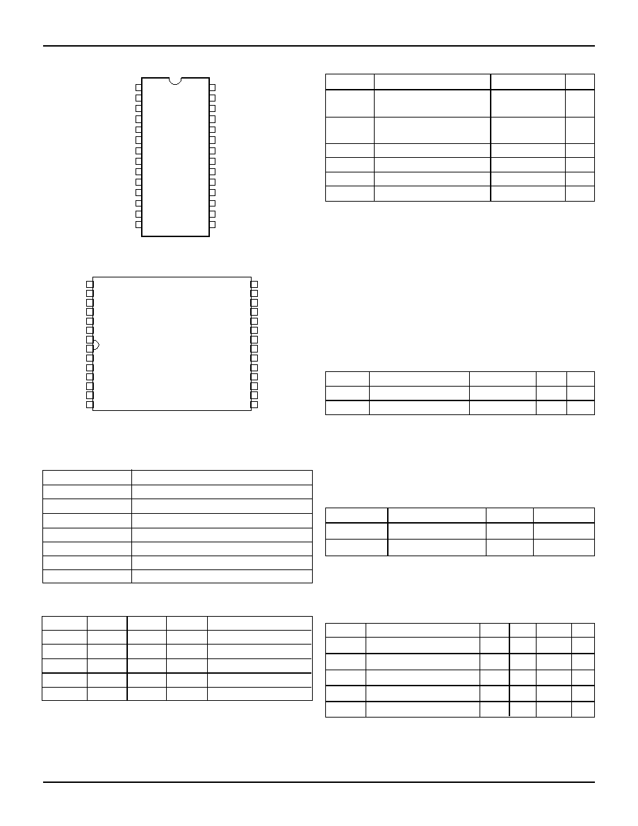
PIN CONFIGURATIONS
ABSOLUTE MAXIMUM RATINGS
(1)
Symbol
Rating
Value
Unit
V
CC
Supply Voltage
≠0.5 to +4.6
V
Relative to GND
V
TERM
(2)
Terminal Voltage
≠0.5 to V
CC
+0.5
V
Relative to GND
T
BIAS
Temperature Under Bias
≠55 to +125
∞
C
T
STG
Storage Temperature
≠55 to +125
∞
C
P
T
Power Dissipation
1.0
W
I
OUT
DC Output Current
50
mA
NOTES:
3101 tbl 03
1. Stresses greater than those listed under ABSOLUTE MAXIMUM
RATINGS may cause permanent damage to the device. This is a stress
rating only and functional operation of the device at these or any other
conditions above those indicated in the operational sections of this
specification is not implied. Exposure to absolute maximum rating
conditions for extended periods may affect reliability.
2. Input, Output, and I/O terminals; 4.6V maximum.
CAPACITANCE
(T
A
= +25
∞
C, f = 1.0MHz, SOJ package)
Symbol
Parameter
(1)
Conditions
Max.
Unit
C
IN
Input Capacitance
V
IN
= 3dV
6
pF
C
OUT
Output Capacitance
V
OUT
= 3dV
7
pF
NOTE:
3101 tbl 04
1. This parameter is determined by device characterization, but is not
production tested.
RECOMMENDED DC OPERATING
CONDITIONS
Symbol
Parameter
Min.
Typ.
Max. Unit
V
CC
Supply Voltage
3.0
3.3
3.6
V
GND
Supply Voltage
0
0
0
V
V
IH
Input High Voltage - Inputs
2.0
--
5.0
V
V
IH
Input High Voltage - I/O
2.0
--
Vcc+0.3
V
V
IL
Input Low Voltage
≠0.3
(1)
--
0.8
V
NOTE:
3101 tbl 06
1. V
IL
(min.) = ≠2.0V for pulse width less than 5ns, once per cycle.
TRUTH TABLE
(1)
WE
WE
CS
CS
OE
OE
I/O
Function
X
H
X
High-Z
Standby (ISB)
X
V
HC
X
High-Z
Standby (ISB1)
H
L
H
High-Z
Output Disable
H
L
L
D
OUT
Read
L
L
X
D
IN
Write
NOTE:
3101 tbl 02
1. H = V
IH
, L = V
IL
, X = Don't Care
3101 drw 02
5
6
7
8
9
10
11
12
A
12
1
2
3
4
24
23
22
21
20
19
18
17
SO28-5
P28-2
13
14
28
27
26
25
A
7
A
6
A
5
A
4
A
3
A
2
A
1
A
0
I/O
0
I/O
1
V
CC
WE
A
8
A
9
A
11
OE
A
10
CS
I/O
7
16
15
I/O
2
GND
I/O
6
I/O
5
I/O
4
I/O
3
A
14
A
13
DIP/SOJ
TOP VIEW
PIN DESCRIPTIONS
Name
Description
A
0
≠A
14
Addresses
I/O
0
≠I/O
7
Data Input/Output
CS
Chip Select
WE
Write Enable
OE
Output Enable
GND
Ground
V
CC
Power
3101 tbl 01
TSOP
TOP VIEW
3101 drw 11
22
23
24
25
26
27
28
1
2
3
4
5
7
6
21
20
19
18
17
16
15
14
13
12
11
10
9
8
A
10
CS
I/O
7
I/O
6
I/O
5
I/O
4
I/O
3
GND
I/O
2
I/O
1
I/O
0
A
0
A
1
A
2
SO28-8
OE
A
11
A
9
A
8
A
13
A
14
A
7
A
6
A
5
A
4
A
3
A
12
WE
V
CC

3
IDT71V256SA
3.3V CMOS STATIC RAM 256K (32K x 8-BIT)
INDUSTRIAL AND COMMERCIAL TEMPERATURE RANGES
DC ELECTRICAL CHARACTERISTICS
V
CC
= 3.3V
±
0.3V
IDT71V256SA
Symbol
Parameter
Test Condition
Min.
Typ.
Max.
Unit
|I
LI
|
Input Leakage Current
V
CC
= Max., V
IN
= GND to V
CC
--
--
2
µ
A
|I
LO
|
Output Leakage Current
V
CC
= Max.,
CS
= V
IH,
V
OUT
= GND to V
CC
--
--
2
µ
A
V
OL
Output Low Voltage
I
OL
= 8mA, V
CC
= Min.
--
--
0.4
V
V
OH
Output High Voltage
I
OH
= ≠4mA, V
CC
= Min.
2.4
--
--
V
3101 tbl 08
DC ELECTRICAL CHARACTERISTICS
(1, 2)
(V
CC
= 3.3V
±
0.3V, V
LC
= 0.2V, V
HC
= V
CC
- 0.2V)
Symbol
Parameter
71V256SA10
(3)
71V256SA12
(3)
71V256SA15 71V256SA20
(3)
Unit
I
CC
Dynamic Operating Current
CS
V
IL
, Outputs
100
90
85
85
mA
Open, V
CC
= Max., f = f
MAX
(2)
I
SB
Standby Power Supply Current (TTL Level)
20
20
20
20
mA
CS
= V
IH
, V
CC
= Max., Outputs Open, f = f
MAX
(2)
I
SB1
Full Standby Power Supply Current (CMOS Level)
2
2
2
2
mA
CS
V
HC
, V
CC
= Max., Outputs Open, f = 0
(2)
,
V
IN
V
LC
or V
IN
V
HC
NOTES:
3101 tbl 07
1. All values are maximum guaranteed values.
2. f
MAX
= 1/t
RC
, only address inputs cycling at fmax; f = 0 means that no inputs are cycling.
3. Commercial temperature range only.
Figure 1. AC Test Load
Figure 2. AC Test Load
(for t
CLZ
, t
OLZ
, t
CHZ
, t
OHZ
, t
OW
, t
WHZ
)
*Includes scope and jig capacitances
AC TEST CONDITIONS
Input Pulse Levels
GND to 3.0V
Input Rise/Fall Times
3ns
Input Timing Reference Levels
1.5V
Output Reference Levels
1.5V
AC Test Load
See Figures 1 and 2
3101 tbl 09
3101 drw 04
320
30pF*
350
DATA
OUT
3.3V
3101 drw 05
320
5pF*
350
DATA
OUT
3.3V
4
IDT71V256SA
3.3V CMOS STATIC RAM 256K (32K x 8-BIT)
INDUSTRIAL AND COMMERCIAL TEMPERATURE RANGES
AC ELECTRICAL CHARACTERISTICS
(V
CC
= 3.3V
±
0.3V)
71V256SA10
(2)
71V256SA12
(2)
71V256SA15
71V256SA20
(2)
Symbol
Parameter
Max.
Min.
Min.
Max.
Min.
Max.
Min.
Max.
Unit
Read Cycle
t
RC
Read Cycle Time
10
--
12
--
15
--
20
--
ns
t
AA
Address Access Time
--
10
--
12
--
15
--
20
ns
t
ACS
Chip Select Access Time
--
10
--
12
--
15
--
20
ns
t
CLZ
(1)
Chip Select to Output in Low-Z
5
--
5
--
5
--
5
--
ns
t
CHZ
(1)
Chip Select to Output in High-Z
0
8
0
8
0
9
0
10
ns
t
OE
Output Enable to Output Valid
--
6
--
6
--
7
--
8
ns
t
OLZ
(1)
Output Enable to Output in Low-Z
3
--
3
--
0
--
0
--
ns
t
OHZ
(1)
Output Disable to Output in High-Z
2
6
2
6
0
7
0
8
ns
t
OH
Output Hold from Address Change
3
--
3
--
3
--
3
--
ns
Write Cycle
t
WC
Write Cycle Time
10
--
12
--
15
--
20
--
ns
t
AW
Address Valid to End-of-Write
9
--
9
--
10
--
15
--
ns
t
CW
Chip Select to End-of-Write
9
--
9
--
10
--
15
--
ns
t
AS
Address Set-up Time
0
--
0
--
0
--
0
--
ns
t
WP
Write Pulse Width
9
--
9
--
10
--
15
--
ns
t
WR
Write Recovery Time
0
--
0
--
0
--
0
--
ns
t
DW
Data to Write Time Overlap
6
--
6
--
7
--
8
--
ns
t
DH
Data Hold from Write Time
0
--
0
--
0
--
0
--
ns
t
OW
(1)
Output Active from End-of-Write
4
--
4
--
4
--
4
--
ns
t
WHZ
(1)
Write Enable to Output in High-Z
1
8
1
8
1
9
1
10
ns
NOTE:
3101 tbl 10
1. This parameter guaranteed with the AC test load (Figure 2) by device characterization, but is not production tested.
2. Commercial temperature range only.
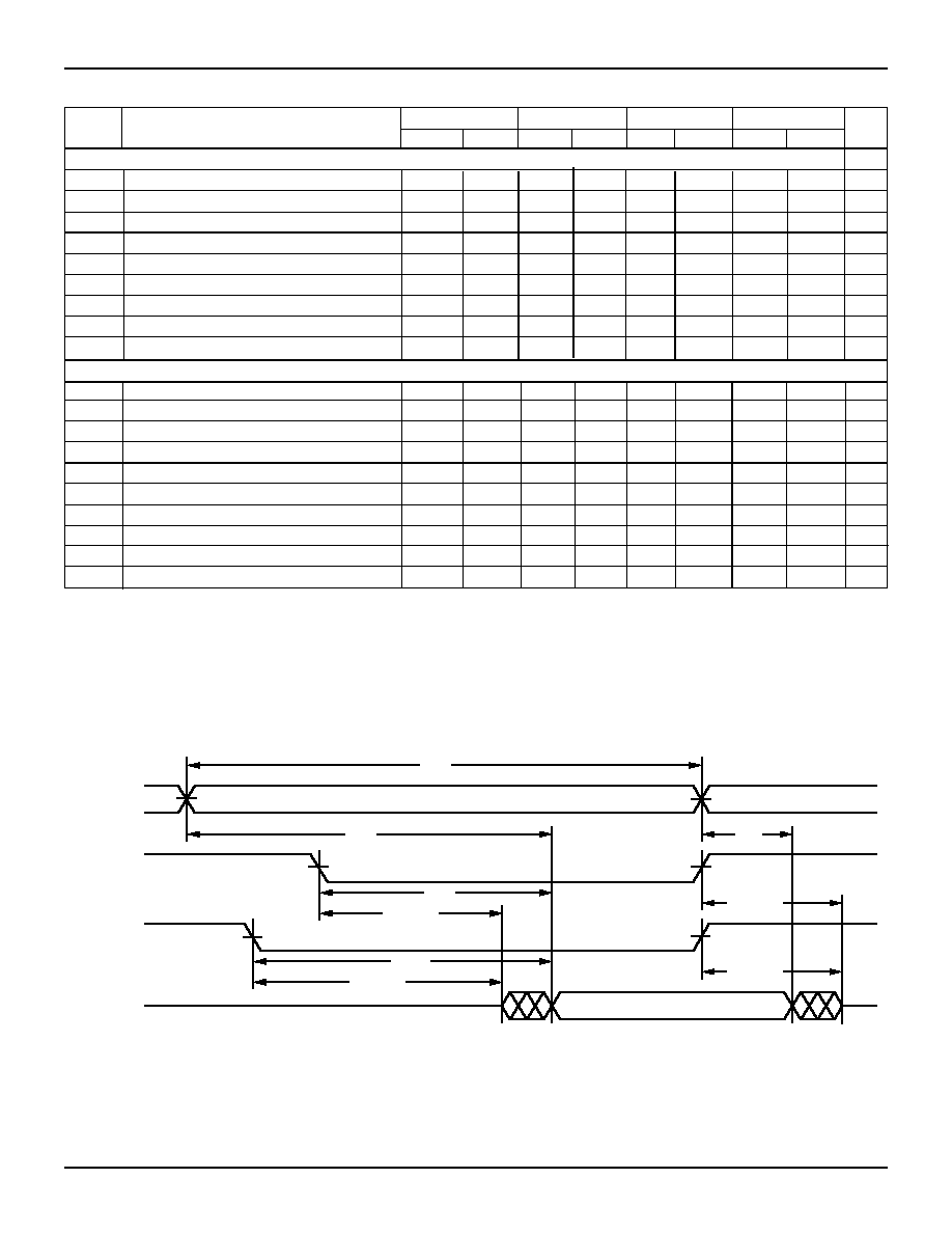
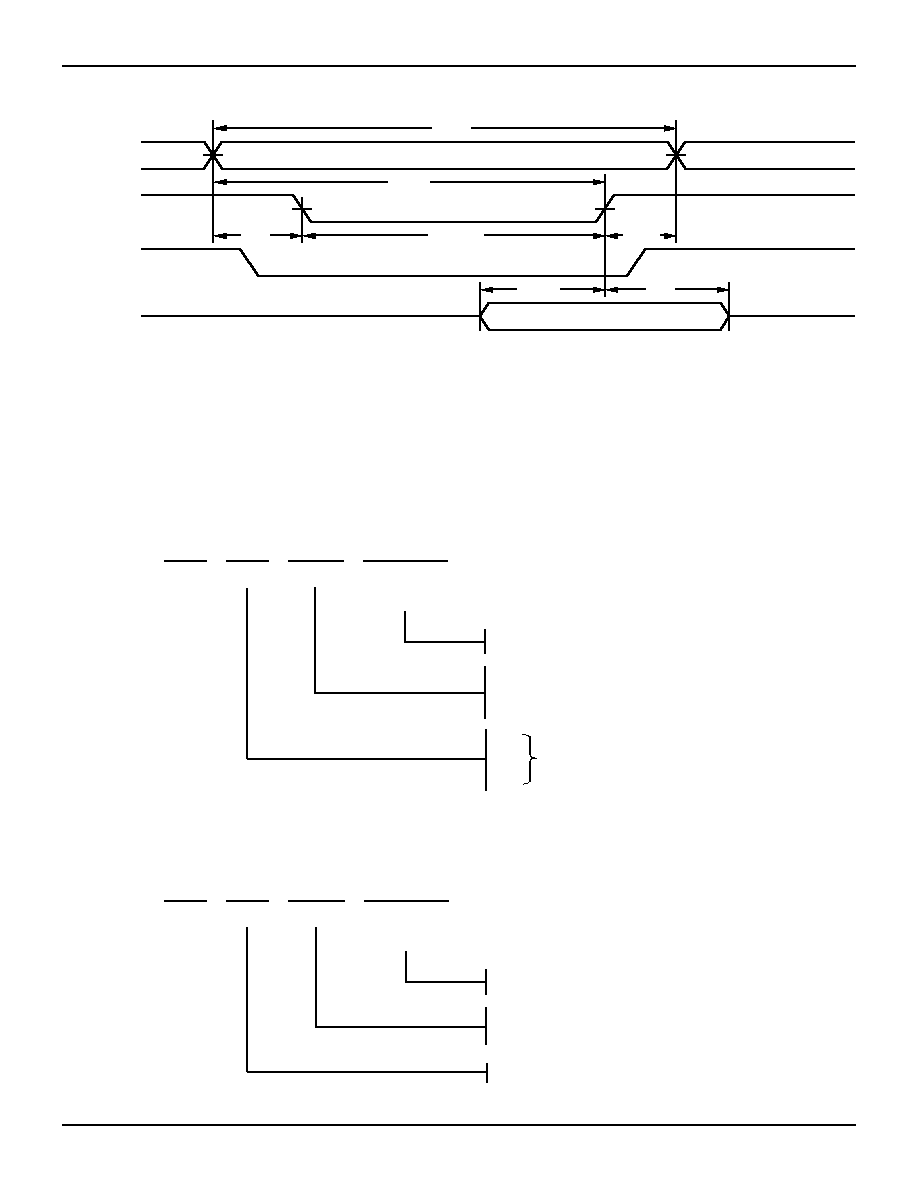
TIMING WAVEFORM OF READ CYCLE NO. 1
(1)
NOTES:
1.
WE
is HIGH for Read cycle.
2. Transition is measured
±
200mV from steady state.
ADDRESS
CS
DATA
OUT
OE
3101 drw 06
t
RC
t
AA
t
OH
t
ACS
t
CLZ
t
CHZ
(2)
t
OE
t
OLZ
(2)
(2)
t
OHZ
(2)
DATA VALID
5
IDT71V256SA
3.3V CMOS STATIC RAM 256K (32K x 8-BIT)
INDUSTRIAL AND COMMERCIAL TEMPERATURE RANGES
TIMING WAVEFORM OF READ CYCLE NO. 2
(1, 2, 4)
TIMING WAVEFORM OF READ CYCLE NO. 3
(1, 3, 4)
NOTES:
1.
WE
is HIGH for Read cycle.
2. Device is continuously selected,
CS
is LOW.
3. Address valid prior to or coincident with
CS
transition LOW.
4.
OE
is LOW.
5. Transition is measured
±
200mV from steady state.
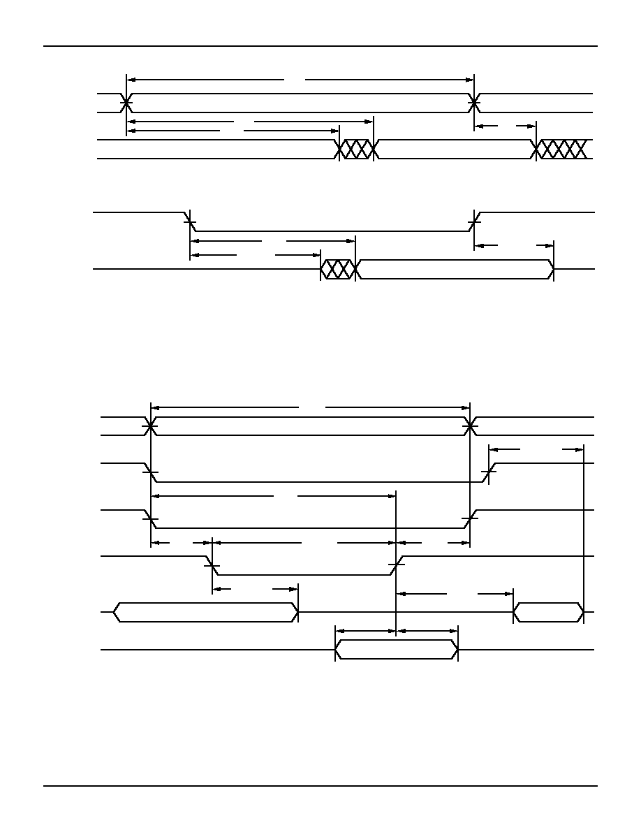
NOTES:
1.
WE
or
CS
must be HIGH during all address transitions.
2. A write occurs during the overlap of a LOW
CS
and a LOW
WE
.
3. t
WR
is measured from the earlier of
CS
or
WE
going HIGH to the end of the write cycle.
4. During this period, I/O pins are in the output state so that the input signals must not be applied.
5. If the
CS
LOW transition occurs simultaneously with or after the
WE
LOW transition, the outputs remain in a high-impedance state.
6. Transition is measured
±
200mV from steady state.
7. If
OE
is LOW during a
WE
controlled write cycle, the write pulse width must be the larger of t
WP
or (t
WHZ
+ t
DW
) to allow the I/O drivers to turn off and data
to be placed on the bus for the required t
DW
. If
OE
is HIGH during a
WE
controlled write cycle, this requirement does not apply and the write pulse can
be as short as the spectified t
WP.
TIMING WAVEFORM OF WRITE CYCLE NO. 1 (
WE
WE
CONTROLLED TIMING)
(1, 2, 3, 5, 7)
ADDRESS
DATA
OUT
3101 drw 07
t
RC
t
AA
t
OH
t
OH
DATA VALID
PREVIOUS DATA VALID
DATA
OUT
CS
3101 drw 08
t
ACS
(5)
t
CLZ
(5)
CHZ
t
DATA VALID
CS
DATA
IN
ADDRESS
WE
DATA
OUT
OE
3101 drw 09
t
AW
t
WR
t
DW
t
WC
t
WP
t
DH
t
WHZ
t
OW
(4)
(7)
t
AS
(6)
(4)
t
OHZ
(6)
DATA VALID
(6)
6
IDT71V256SA
3.3V CMOS STATIC RAM 256K (32K x 8-BIT)
INDUSTRIAL AND COMMERCIAL TEMPERATURE RANGES
TIMING WAVEFORM OF WRITE CYCLE NO. 2 (
CS
CS
CONTROLLED TIMING)
(1, 2, 3, 4)
NOTES:
1.
WE
or
CS
must be HIGH during all address transitions.
2. A write occurs during the overlap of a LOW
CS
and a LOW
WE
.
3. t
WR
is measured from the earlier of
CS
or
WE
going HIGH to the end of the write cycle.
4. If the
CS
LOW transition occurs simultaneously with or after the
WE
LOW transition, the outputs remain in a high-impedance state.
5. If
OE
is LOW during a
WE
controlled write cycle, the write pulse width must be the larger of t
WP
or (t
WHZ
+ t
DW
) to allow the I/O drivers to turn off and data
to be placed on the bus for the required t
DW
. If
OE
is HIGH during a
WE
controlled write cycle, this requirement does not apply and the write pulse can
be as short as the spectified t
WP.
ORDERING INFORMATION - COMMERCIAL
CS
DATA
IN
ADDRESS
WE
t
WR
3101 drw 10
t
AW
t
DW
t
WC
t
CW
t
DH
AS
t
t
(5)
DATA VALID
300 mil SOJ (SO28-5)
300 mil Plastic DIP (P28-2)
TSOP Type I (SO28-8)
SA
Power
XX
Speed
X
Package
X
Process/
Temperature
Range
Blank
Commercial (0
∞
C to +70
∞
C)
Y
TP
PZ
IDT71V256
10
12
15
20
Speed in nanoseconds
3101 drw 11
300 mil SOJ (SO28-5)
TSOP Type I (SO28-8)
SA
Power
XX
Speed
X
Package
X
Process/
Temperature
Range
I
Industrial (-40
∞
C to +85
∞
C)
Y
PZ
IDT71V256
15
Speed in nanoseconds
3101 drw 12
ORDERING INFORMATION - INDUSTRIAL