 | –≠–ª–µ–∫—Ç—Ä–æ–Ω–Ω—ã–π –∫–æ–º–ø–æ–Ω–µ–Ω—Ç: MK3732-07 | –°–∫–∞—á–∞—Ç—å:  PDF PDF  ZIP ZIP |

MDS 3732-07 F
1
Revision 100102
Integrated Circuit Systems, Inc.
q
525 Race Street, San Jose, CA 95126
q
tel (408) 295-9800
q
www.icst.com
ADSL VCXO C
LOCK
S
OURCE
MK3732-07
Description
The MK3732-07 is a low cost, low jitter, high
performance VCXO and PLL clock synthesizer
designed to replace expensive VCXO modules and
oscillators. The on-chip Voltage Controlled Crystal
Oscillator (VCXO) accepts a 0 to 3.3 V input voltage to
cause the output clocks to vary by +100 ppm. Using
ICS' patented VCXO and analog Phase-Locked Loop
(PLL) techniques, the device uses an inexpensive
13.248 MHz pullable crystal input to produce one or
two output clocks.
The MK3732-07 is a pin-to-pin replacement for the
MK2732-07 when using +3.3V supply voltage.
ICS manufactures the largest variety of xDSL clock
synthesizers for all applications. Consult ICS to
eliminate VCXOs, crystals, and oscillators from your
board.
Features
∑
Packaged in 16 pin (150 mil) SOIC
∑
Replaces a VCXO and oscillator
∑
Ideal for Asymmetrical Digital Subscriber Line
(ADSL) chipsets
∑
Uses an inexpensive pullable crystal
∑
On-chip patented VCXO with pull range of 200 ppm
(+ 100 ppm) minimum
∑
VCXO tuning voltage of 0 to 3.3 V
∑
12 mA output drive capability at TTL levels
∑
Advanced, low power, sub-micron CMOS process
∑
Operating voltage of 3.3V
∑
Industrial temperature range available
Block Diagram
V o lta g e
C o n tro lle d
C ry s ta l
O s c illa to r
X 1
X 2
V I N
1 3 . 2 4 8 M H z
P u l l a b l e
C r y s t a l
P L L /
C lo c k
S y n th e s is
C irc u itry
C L K 1
C L K 2
S 2 : S 0
V D D
G N D
O E
3
3
3
ADSL VCXO C
LOCK
S
OURCE
MDS 3732-07 F
2
Revision 100102
Integrated Circuit Systems, Inc.
q
525 Race Street, San Jose, CA 95126
q
tel (408) 295-9800
q
www.icst.com
MK3732-07
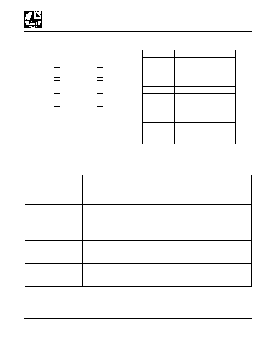
Pin Assignment
Clock Select Table
0=connect directly to GND
M=leave unconnected (floating)
1=connect directly to VDD
Pin Descriptions
12
1
11
2
10
3
9
X2
4
X1
5
VD D
6
N C
7
VIN
8
VD D
G N D
V D D
G N D
G N D
S 0
S 2
C LK1
O E
16
15
14
13
C LK2
S 1
16 P in (150 m il) S O IC
S2
S1
S0
Input
CLK1
CLK2
0
0
0
13.248
35.328
29.4
0
0
M
13.248
35.328
47.1
0
0
1
13.248
35.328
40.4
0
1
0
13.248
42.4
35.328
0
1
M
Test
Test
Test
0
1
1
Test
Test
Test
1
0
0
Test
Test
Test
1
0
M
Test
Test
Test
1
0
1
13.248
35.328
Off
1
1
0
13.248
2.208
Off
1
1
M
13.248
24.73
35.328
1
1
1
13.248
49.46
35.328
Pin
Number
Pin
Name
Pin
Type
Pin Description
1
X2
Input
Crystal connection. Connect to a pullable crystal of 13.248 MHz.
2
X1
Input
Crystal connection. Connect to a pullable crystal of 13.248 MHz.
3,5,13
VDD
Power
Connect to +3.3V.
4
VIN
Input
Voltage input to VCXO. Zero to 3.3V signal which controls the VCXO
frequency.
6,12,14
GND
Power
Connect to ground.
7
CLK1
Output
Clock output #1 per table above.
8
CLK2
Output
Clock output #2 per table above.
9
S2
Input
Select input #2. Selects outputs per table above. Internal pull-up resistor.
10
OE
Input
Output enable. Tri-states outputs when low. Internal pull-up resistor.
11
S0
Input
Select input #0. Selects outputs per table above.
15
NC
-
No connect. Do not connect anything to this pin.
16
S1
Input
Select input #1. Selects outputs per table above.

ADSL VCXO C
LOCK
S
OURCE
MDS 3732-07 F
3
Revision 100102
Integrated Circuit Systems, Inc.
q
525 Race Street, San Jose, CA 95126
q
tel (408) 295-9800
q
www.icst.com
MK3732-07
External Component Selection
The MK3732-07 requires a minimum number of
external components for proper operation.
Decoupling Capacitors
Decoupling capacitors of 0.01
µ
F should be connected
between VDD and GND on pins 3 and 6, on pins 5 and
6, and on pins 13 and 14, as close to the MK3732-07
as possible. For optimum device performance, the
decoupling capacitors should be mounted on the
component side of the PCB. Avoid the use of vias in the
decoupling circuit.
Series Termination Resistor
When the PCB traces between the clock outputs and
the loads are over 1 inch, series termination should be
used. To series terminate a 50
trace (a commonly
used trace impedance) place a 33
resistor in series
with the clock line, as close to the clock output pin as
possible. The nominal impedance of the clock output is
20
.
Quartz Crystal
The MK3732-07 VCXO function consists of the
external crystal and the integrated VCXO oscillator
circuit. To assure the best system performance
(frequency pull range) and reliability, a crystal device
with the recommended parameters must be used, and
the layout guidelines discussed in the following section
must be followed.
The frequency of oscillation of a quartz crystal is
determined by its "cut" and by the load capacitors
connected to it. The MK3732-07 incorporates on-chip
variable load capacitors that "pull" (change) the
frequency of the crystal. The crystal specified for use
with the MK3732-07 is designed to have zero
frequency error when the total of on-chip + stray
capacitance is 14pF.
The external crystal must be connected as close to the
chip as possible and should be on the same side of the
PCB as the MK3732-07. There should be no via's
between the crystal pins and the X1 and X2 device
pins. There should be no signal traces underneath or
close to the crystal.
Please see application note MAN05 for recommended
crystal parameters and suppliers.
Crystal Tuning Load Capacitors
The crystal traces should include pads for small fixed
capacitors, one between X1 and ground, and another
between X2 and ground. Stuffing of these capacitors
on the PCB is optional. The need for these capacitors
is determined at system prototype evaluation, and is
influenced by the particular crystal used (manufacture
and frequency) and by PCB layout. The typical required
capacitor value is 1 to 4 pF.
To determine the need for and value of the crystal
adjustment capacitors, you will need a PC board of
your final layout, a frequency counter capable of about
1 ppm resolution and accuracy, two power supplies,
and some samples of the crystals which you plan to
use in production, along with measured initial accuracy
for each crystal at the specified crystal load
capacitance, CL.
To determine the value of the crystal capacitors:
1. Connect VDD of the MK3732-07 to 3.3V. Connect
pin 4 of the MK3732-07 to the second power supply.
Adjust the voltage on pin 4 to 0V. Measure and record
the frequency of the CLK output.
2. Adjust the voltage on pin 4 to 3.3V. Measure and
record the frequency of the same output.
To calculate the centering error:
Where:
f
target
= nominal crystal frequency
error
xtal
=actual initial accuracy (in ppm) of the crystal
being measured
If the centering error is less than ±25 ppm, no
adjustment is needed. If the centering error is more
than 25ppm negative, the PC board has excessive
stray capacitance and a new PCB layout should be
considered to reduce stray capacitance. (Alternately,
the crystal may be re-specified to a higher load
capacitance. Contact ICS for details.) If the centering
error is more than 25ppm positive, add identical fixed
centering capacitors from each crystal pin to ground.
The value for each of these caps (in pF) is given by:
Error
10
6
x
f
3.3
V
f
t
et
arg
≠
(
)
f
0V
f
t
et
arg
≠
(
)
+
f
t
et
arg
------------------------------------------------------------------------------
error
xtal
≠
=
ADSL VCXO C
LOCK
S
OURCE
MDS 3732-07 F
4
Revision 100102
Integrated Circuit Systems, Inc.
q
525 Race Street, San Jose, CA 95126
q
tel (408) 295-9800
q
www.icst.com
MK3732-07
External Capacitor =
2 x (centering error)/(trim sensitivity)
Trim sensitivity is a parameter which can be supplied
by your crystal vendor. If you do not know the value,
assume it is 30 ppm/pF. After any changes, repeat the
measurement to verify that the remaining error is
acceptably low (typically less than ±25ppm).
Absolute Maximum Ratings
Stresses above the ratings listed below can cause permanent damage to the MK3732-07. These ratings,
which are standard values for ICS commercially rated parts, are stress ratings only. Functional operation of
the device at these or any other conditions above those indicated in the operational sections of the
specifications is not implied. Exposure to absolute maximum rating conditions for extended periods can
affect product reliability. Electrical parameters are guaranteed only over the recommended operating
temperature range.
Recommended Operation Conditions
DC Electrical Characteristics
VDD=3.3V ±5%
, Ambient temperature 0 to +70
∞
C, unless stated otherwise
Item
Rating
Supply Voltage, VDD
7V
All Inputs and Outputs
-0.5V to VDD+0.5V
Ambient Operating Temperature
-40 to +85
∞
C
Storage Temperature
-65 to +150
∞
C
Soldering Temperature
260
∞
C
Parameter
Min.
Typ.
Max.
Units
Ambient Operating Temperature
-40
≠
+85
∞
C
Power Supply Voltage (measured in respect to GND)
+3.15
+3.45
V
Reference crystal parameters
Refer to page 3
Parameter
Symbol
Conditions
Min.
Typ.
Max.
Units
Operating Voltage
VDD
3.15
3.3
3.45
V
Output High Voltage
V
OH
I
OH
= -12 mA
2.4
V
Output Low Voltage
V
OL
I
OL
= 12 mA
0.4
V
Output High Voltage (CMOS
Level)
V
OH
I
OH
= -8 mA
VDD-0.4
V
Input High Voltage, binary
inputs
V
IH
S2, S1, OE
2.0
V
Input High Voltage, trinary input
V
IH
S0
VDD-0.5
V
Input Low Voltage, binary
inputs
V
IL
S2, S1, OE
0.8
V
ADSL VCXO C
LOCK
S
OURCE
MDS 3732-07 F
5
Revision 100102
Integrated Circuit Systems, Inc.
q
525 Race Street, San Jose, CA 95126
q
tel (408) 295-9800
q
www.icst.com
MK3732-07
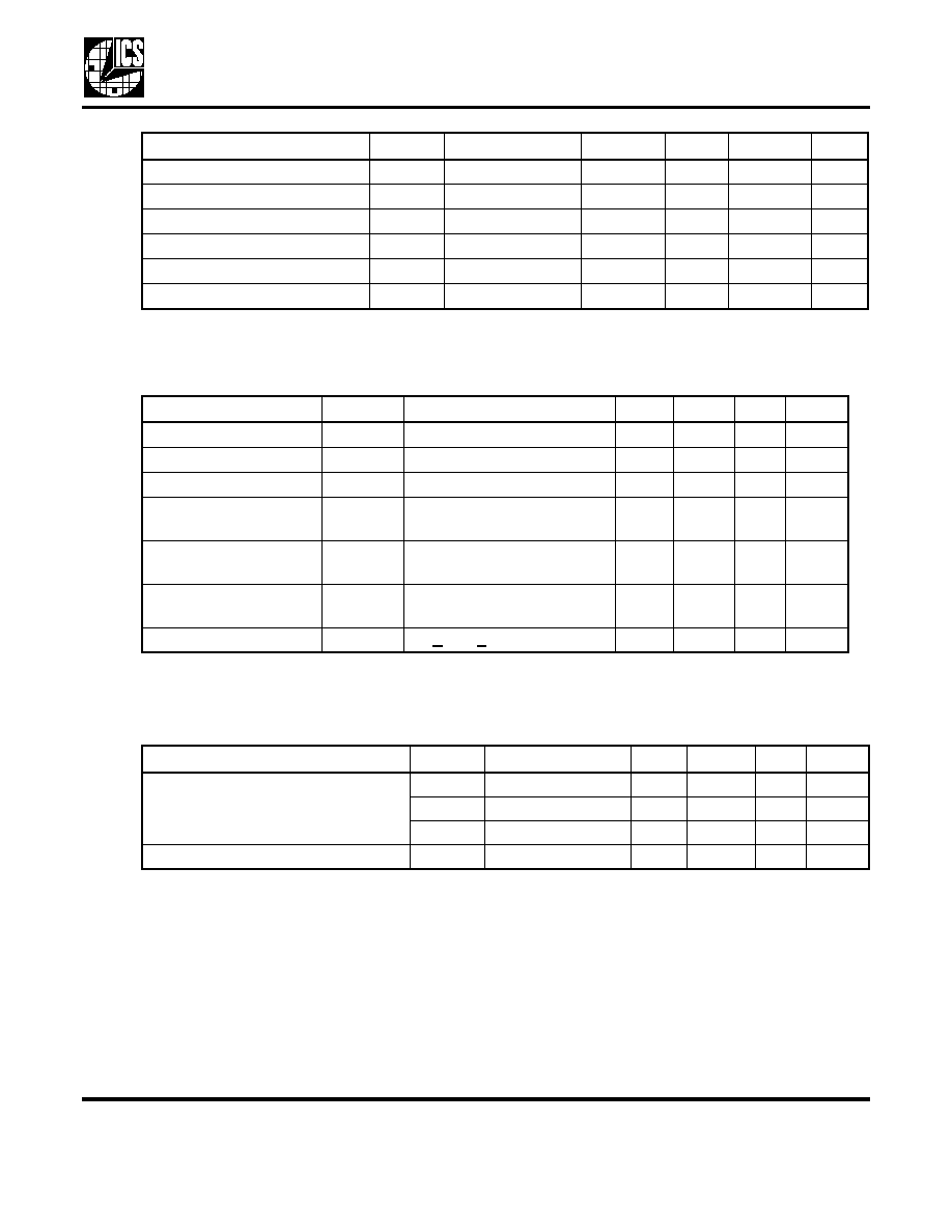
AC Electrical Characteristics
VDD = 3.3V ±5%
, Ambient Temperature 0 to +70
∞
C, unless stated otherwise
Note 1: External pullable crystal must conform with those listed in application note MAN05
Thermal Characteristics
Input Low Voltage, trinary input
V
IL
S0
0.5
V
Operating Supply Current
IDD
No load
12
mA
Short Circuit Current
I
OS
±50
mA
Input Capacitance
S2:S0, OE
5
pF
Frequency synthesis error
Both clocks
0
ppm
VIN, VCXO Control Voltage
V
IA
0
3.3
V
Parameter
Symbol
Conditions
Min.
Typ.
Max.
Units
Input Crystal Frequency
f
in
13.248
MHz
Output Clock Rise Time
t
OR
0.8 to 2.0V
1.5
ns
Output Clock Fall Time
t
OF
2.0 to 0.8V
1.5
ns
Output Clock Duty
Cycle
t
D
At VDD/2
40
60
%
Maximum Absolute
Jitter
t
j
±150
ps
Phase Noise, relative to
carrier
10 kHz offset
-115
dBc/Hz
Output pullability, note 1
f
P
0V < VIN < 3.3V
±100
ppm
Parameter
Symbol
Conditions
Min.
Typ.
Max.
Units
Thermal Resistance Junction to
Ambient
JA
Still air
120
∞
C/W
JA
1 m/s air flow
115
∞
C/W
JA
3 m/s air flow
105
∞
C/W
Thermal Resistance Junction to Case
JC
58
∞
C/W
Parameter
Symbol
Conditions
Min.
Typ.
Max.
Units

ADSL VCXO C
LOCK
S
OURCE
MDS 3732-07 F
6
Revision 100102
Integrated Circuit Systems, Inc.
q
525 Race Street, San Jose, CA 95126
q
tel (408) 295-9800
q
www.icst.com
MK3732-07
Package Outline and Package Dimensions (16 pin SOIC)
Package dimensions are kept current with JEDEC Publication No. 95
Ordering Information
While the information presented herein has been checked for both accuracy and reliability, Integrated Circuit Systems (ICS)
assumes no responsibility for either its use or for the infringement of any patents or other rights of third parties, which would
result from its use. No other circuits, patents, or licenses are implied. This product is intended for use in normal commercial
applications. Any other applications such as those requiring extended temperature range, high reliability, or other extraordinary
environmental requirements are not recommended without additional processing by ICS. ICS reserves the right to change any
circuitry or specifications without notice. ICS does not authorize or warrant any ICS product for use in life support devices or
critical medical instruments.
Part / Order Number
(Note 1)
Marking
Shipping
packaging
Package
Temperature
MK3732-07S
MK3732-07S
Tubes
16 pin SOIC
0 to +70
∞
C
MK3732-07STR
MK3732-07S
Tape and Reel
16 pin SOIC
0 to +70
∞
C
MK3732-07SI
MK3732-07SI
Tubes
16 pin SOIC
-40 to +85
∞
C
MK3732-07SITR
MK3732-07SI
Tape and Reel
16 pin SOIC
-40 to +85
∞
C
INDEX
AREA
1 2
16
D
E
SEATING
PLANE
A1
A
e
- C -
B
.10 (.004)
C
C
L
H
h x 45
Millimeters
Inches
Symbol
Min
Max
Min
Max
A
1.35
1.75
.0532
.0688
A1
0.10
0.25
.0040
.0098
B
0.33
0.51
.013
.020
C
0.19
0.25
.0075
.0098
D
9.80
10.00
.3859
.3937
E
3.80
4.00
.1497
.1574
e
1.27 BASIC
0.050 BASIC
H
5.80
6.20
.2284
.2440
h
0.25
0.50
.010
.020
L
0.40
1.27
.016
.050
0
∞
8
∞
0
∞
8
∞