 | –≠–ª–µ–∫—Ç—Ä–æ–Ω–Ω—ã–π –∫–æ–º–ø–æ–Ω–µ–Ω—Ç: MK2069-03 | –°–∫–∞—á–∞—Ç—å:  PDF PDF  ZIP ZIP |

MK2069-03
MDS 2069-03 I
1
Revision 050203
Integrated Circuit Systems, Inc.
l
525 Race Street, San Jose, CA 95126
l
tel (408) 295-9800
l
www.icst.com
VCXO-Based Clock Translator with High Multiplication
Description
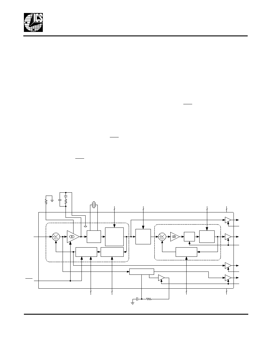
The MK2069-03 is a VCXO (Voltage Controlled Crystal
Oscillator) based clock generator that offers system
synchronization, jitter attenuation and frequency
translation. It can accept an input clock over a wide
range of frequencies and produces a de-jittered, low
phase noise clock output. The device is optimized for
user configuration by providing access to all major PLL
divider functions. No power-up programming is needed
as configuration is pin selected. External VCXO loop
filter components provide an additional level of
performance tailoring.
The MK2069-03 features a very wide range VCXO PLL
feedback divider, allowing high frequency multiplication
ratios and therefore the input of very low input
reference frequencies. The lock detector (LD) output
serves as a clock status monitor. The clear (CLR) input
enables rapid synchronization to the phase of a newly
selected input clock, while eliminating the generation of
extra clock cycles and wander caused by memory in
the PLL feedback divider. CLR also serves as a
temporary holdover function when kept low.
Features
∑
Wide range VCXO PLL feedback divider allows high
frequency multiplication ratios and the input of very
low input reference frequencies
∑
Input clock frequency of <1kHz to 13.5MHz
∑
Output clock frequency of 500kHz to 160MHz
∑
PLL lock status output
∑
VCXO-based clock generation offers very low jitter
and phase noise generation, even with low frequency
or jittery input clock.
∑
PLL Clear function (CLR input) allows the VCXO to
free-run, offering a short term holdover function.
∑
2nd PLL provides frequency translation of VCXO
PLL to higher or alternate output frequencies.
∑
Device will free-run in the absence of an input clock
(or stopped input clock) based on the VCXO
frequency pulled to minimum frequency limit.
∑
Low power CMOS technology
∑
56 pin TSSOP package
∑
Single 3.3V power supply
Block Diagram
C harge
P um p
V C X O
P u lla b le
x ta l
V C L K
X 2
X 1
IS E T
4
V D D
4
C L R
L F
F V D iv id e r
1 to 4 0 9 6
S V
D iv id e r
1 ,2 ,4 ,6 ,8 ,
1 0 ,1 2 ,1 6
IC L K
R T
D iv id e r
1 to 4
P hase
D etector
V C X O
P L L
F T D iv id e r
1 to 6 4
S T
D iv id e r
2 ,4 ,8 ,1 6
V C O
T ra n s la to r
P L L
S V 2 :0
3
F V 1 1 :0
F T 5 :0
6
S T 1 :0
2
T C L K
O E V
O E T
L D
O E L
G N D
R C L K
O E R
L o c k D e te c to r
12
L D C
L D R
L F R
R T 1 :0
2
F P V D iv id e r
2 to 6 5
F P V 5 :0
6

VCXO-Based Clock Translator with High Multiplication
MDS 2069-03 I
2
Revision 050203
Integrated Circuit Systems, Inc.
l
525 Race Street, San Jose, CA 95126
l
tel (408) 295-9800
l
www.icst.com
MK2069-03
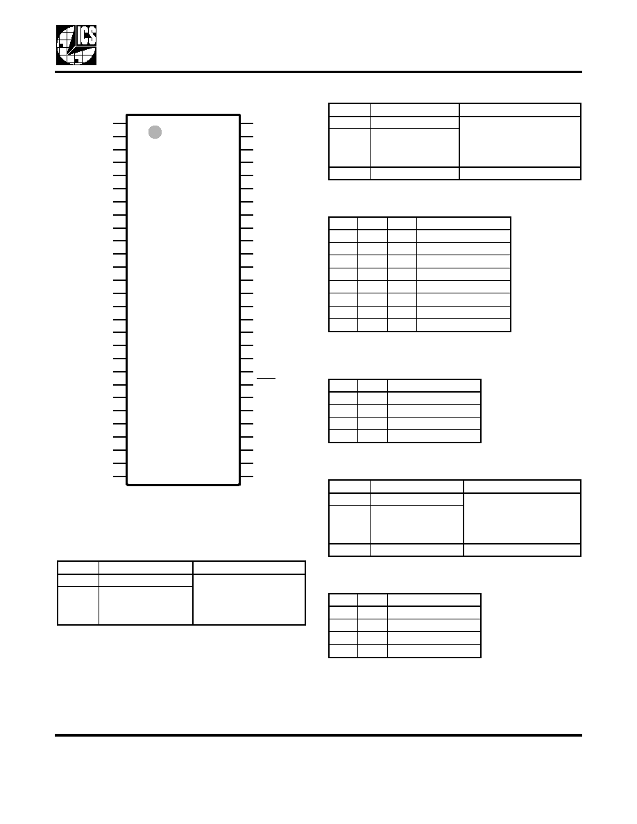
Pin Assignment
VCXO PLL Feedback Pre-Divider Selection
VCXO PLL Feedback Divider Selection
VCXO PLL Scaling Divider Selection Table
Translator PLL Reference Divider Selection
Table
Translator PLL Feedback Divider Selection
Translator PLL Scaling Divider Selection Table
FPV5:0 FPV Divider Ratio
Notes
000000
2
FPV Divide = Address + 2
000001
3
:
:
111111
65
2 1
F V 0
2 2
F V 1
2 3
F V 2
2 4
F V 3
1
S T 0
2
S T 1
3
R T 0
4
R T 1
5
F T 0
6
F T 1
7
F T 2
8
F T 3
9
F T 4
1 0
F T 5
1 1
F P V 0
1 2
V D D T
1 3
G N D T
1 4
X 1
1 5
V D D V
1 6
X 2
1 7
G N D V
1 8
L F R
1 9
L F
2 0
IS E T
2 5
F V 4
2 6
F V 5
2 7
F V 6
2 8
F V 7
3 6
3 5
3 4
3 3
5 6
5 5
5 4
5 3
5 2
5 1
5 0
4 9
4 8
4 7
4 6
4 5
4 4
4 3
4 2
4 1
4 0
3 9
3 8
3 7
3 2
3 1
3 0
2 9
C L R
IC L K
F P V 2
F P V 1
S V 2
S V 1
S V 0
F P V 5
F P V 4
F P V 3
O E L
O E T
O E V
O E R
V D D
L D
T C L K
V D D P
V C L K
G N D P
R C L K
L D R
G N D
L D C
F V 1 1
F V 1 0
F V 9
F V 8
M
K
2069-
0
3
FV11:0 FV Divider Ratio
Notes
0...00
2
For FV addresses 0 to 4094,
FV Divide = Address + 2
0...01
3
:
:
1...10
4096
1...11
1
SV2
SV1
SV0
SV Divider Ratio
0
0
0
4
0
0
1
6
0
1
0
8
0
1
1
10
1
0
0
12
1
0
1
2
1
1
0
16
1
1
1
1
RT1
RT0
RT Divider Ratio
0
0
2
0
1
3
1
0
4
1
1
1
FT5:0
FT Divider Ratio
Notes
000000
2
For FT addresses 0 to 62,
FT Divide = Address + 2
000001
3
:
:
111110
64
111111
1
ST1
ST0
ST Divider Ratio
0
0
2
0
1
4
1
0
8
1
1
16

VCXO-Based Clock Translator with High Multiplication
MDS 2069-03 I
3
Revision 050203
Integrated Circuit Systems, Inc.
l
525 Race Street, San Jose, CA 95126
l
tel (408) 295-9800
l
www.icst.com
MK2069-03
Pin Descriptions
Pin
Number
Pin
Name
Pin
Type
Pin Description
1
ST0
Input
Scaling Divider bit 0 input, Translator PLL (internal pull-up).
2
ST1
Input
Scaling Divider bit 1 input, Translator PLL (internal pull-up).
3
RT0
Input
Reference Divider bit 0 input, Translator PLL (internal pull-up).
4
RT1
Input
Reference Divider bit 1 input, Translator PLL (internal pull-up).
5
FT0
Input
Feedback Divider bit 0 input, Translator PLL (internal pull-up).
6
FT1
Input
Feedback Divider bit 1 input, Translator PLL (internal pull-up).
7
FT2
Input
Feedback Divider bit 2 input, Translator PLL (internal pull-up).
8
FT3
Input
Feedback Divider bit 3 input, Translator PLL (internal pull-up).
9
FT4
Input
Feedback Divider bit 4 input, Translator PLL (internal pull-up).
10
FT5
Input
Feedback Divider bit 5 input, Translator PLL (internal pull-up).
11
FPV0
Input
Feedback Pre-Divider bit 0 input, VCXO PLL (internal pull-up).
12
VDDT
Power
Power Supply connection for Translator PLL.
13
GNDT
Ground
Ground connection for Translator PLL.
14
X1
-
Crystal oscillator input. Connect this pin to the external quartz crystal.
15
VDDV
Power
Power Supply connection for VCXO PLL.
16
X2
-
Crystal oscillator output. Connect this pin to the external quartz crystal.
17
GNDV
Ground
Ground connection for VCXO PLL.
18
LFR
-
Loop filter connection, reference node. Refer to loop filter circuit on page 6.
19
LF
-
Loop filter connection, active node. Refer to loop filter circuit on page 6.
20
ISET
-
Charge pump current setting pin. Refer to loop filter circuit on page 6.
21
FV0
Input
Feedback Divider bit 0 input, VCXO PLL (internal pull-up).
22
FV1
Input
Feedback Divider bit 1input, VCXO PLL (internal pull-up).
23
FV2
Input
Feedback Divider bit 2 input, VCXO PLL (internal pull-up).
24
FV3
Input
Feedback Divider bit 3 input, VCXO PLL (internal pull-up).
25
FV4
Input
Feedback Divider bit 4 input, VCXO PLL (internal pull-up).
26
FV5
Input
Feedback Divider bit 5 input, VCXO PLL (internal pull-up).
27
FV6
Input
Feedback Divider bit 6 input, VCXO PLL (internal pull-up).
28
FV7
Input
Feedback Divider bit 7 input, VCXO PLL (internal pull-up).
29
FV8
Input
Feedback Divider bit 8 input, VCXO PLL (internal pull-up).
30
FV9
Input
Feedback Divider bit 9 input, VCXO PLL (internal pull-up).
31
FV10
Input
Feedback Divider bit 10 input, VCXO PLL (internal pull-up).
32
FV11
Input
Feedback Divider bit 11 input, VCXO PLL (internal pull-up).
33
FPV1
Input
Feedback Pre-Divider bit 1 input, VCXO PLL (internal pull-up).
34
FPV2
Input
Feedback Pre-Divider bit 2 input, VCXO PLL (internal pull-up).
35
ICLK
Input
Reference clock input, 5V tolerant input
36
CLR
Input
Clear input, allows VCXO to free-run when low (internal pull-up).
37
LDC
-
Lock detector threshold setting circuit connection. Refer to circuit on page 10.
38
GND
Ground
Ground connection for internal digital circuitry.
39
LDR
Power
Lock detector threshold setting circuit connection. Refer to circuit on page 10.
40
RCLK
Output
VCXO PLL Reference Clock output.
41
GNDP
Ground
Ground connection for output drivers (VCLK, TCLK, RCLK, LD, LDR).

VCXO-Based Clock Translator with High Multiplication
MDS 2069-03 I
4
Revision 050203
Integrated Circuit Systems, Inc.
l
525 Race Street, San Jose, CA 95126
l
tel (408) 295-9800
l
www.icst.com
MK2069-03
Functional Description
The MK2069-03 is a PLL (Phase Locked Loop) based
clock generator that generates output clocks
synchronized to an input reference clock. It contains
two cascaded PLL's with user selectable divider ratios.
The first PLL is VCXO-based and uses an external
pullable crystal as part of the normal "VCO" (voltage
controlled oscillator) function of the PLL. The use of a
VCXO assures a low phase noise clock source even
when a low PLL loop bandwidth is implemented. A low
loop bandwidth is needed when the input reference
frequency at the phase detector is low, or when jitter
attenuation of the input reference is desired.
The second PLL is used to translate or multiply the
frequency of the VCXO PLL which has a maximum
output frequency of 27 MHz. This second PLL, or
Translator PLL, uses an on-chip VCO circuit that can
provide an output clock up to 160 MHz. The Translator
PLL uses a high loop bandwidth (typically greater than
1 MHz) to assure stability of the clock output generated
by the VCO. It requires a stable, high frequency input
reference which is provided by the VCXO.
The divide values of the divider blocks within both PLLs
are set by device pin configuration. This enables the
system designer to define the following:
∑
Input clock frequency
∑
VCXO crystal frequency
∑
VCLK output frequency
∑
TCLK output frequency
Any unused clock or logic outputs can be tri-stated to
reduce interference (jitter, phase noise) on other clock
outputs. Outputs can also be tri-stated for system
testing purposes.
External components are used to configure the VCXO
PLL loop response. This serves to maximize loop
stability and to achieve the desired input clock jitter
attenuation characteristics.
42
VCLK
Output
Clock output from VCXO PLL
43
VDDP
Power
Power Supply for output drivers (VCLK, TCLK, RCLK, LD, LDR).
44
TCLK
Output
Clock output from Translator PLL
45
LD
Output
Lock detector output.
46
VDD
Power
Power Supply connection for internal digital circuitry.
47
OER
Input
Output enable for RCLK. RCLK is tri-stated when low (internal pull-up).
48
OEV
Input
Output enable for VCLK. VCLK is tri-stated when low (internal pull-up).
49
OET
Input
Output enable for TCLK. TCLK is tri-stated when low (internal pull-up).
50
OEL
Input
Output enable for LD. LD is tri-stated when low (internal pull-up).
51
FPV3
Input
Feedback Pre-Divider bit 3 input, VCXO PLL (internal pull-up).
52
FPV4
Input
Feedback Pre-Divider bit 4 input, VCXO PLL (internal pull-up).
53
FPV5
Input
Feedback Pre-Divider bit 5 input, VCXO PLL (internal pull-up).
54
SV0
Input
Scaler Divider bit 0 input, VCXO PLL (internal pull-up).
55
SV1
Input
Scaler Divider bit 1 input, VCXO PLL (internal pull-up).
56
SV2
Input
Scaler Divider bit 2 input, VCXO PLL (internal pull-up).
Pin
Number
Pin
Name
Pin
Type
Pin Description

VCXO-Based Clock Translator with High Multiplication
MDS 2069-03 I
5
Revision 050203
Integrated Circuit Systems, Inc.
l
525 Race Street, San Jose, CA 95126
l
tel (408) 295-9800
l
www.icst.com
MK2069-03
Application Information
The MK2069-03 is a mixed analog / digital integrated
circuit that is sensitive to PCB (printed circuit board)
layout and external component selection. Used
properly, the device will provide the same high
performance expected from a canned VCXO-based
hybrid timing device, but at a lower cost. To help avoid
unexpected problems, the guidance provided in the
sections below should be followed.
Setting VCLK Output Frequency
The frequency of the VCLK output is determined by the
following relationship:
Where:
FPV Divider = 2 to 65
FV Divider = 1 to 4096
VCLK output frequency range is set by the allowable
frequency range of the external VCXO crystal and by
the internal VCXO divider selections:
Where:
f(VCXO) = F(External Crystal) = 8 to 27 MHz
SV Divider = 1,2,4,6,8,10,12 or 16
FPV Divider = 2 to 65
A higher crystal frequency will generally produce lower
phase noise and therefore is preferred. A crystal
frequency between 13.5 MHz and 27 MHz is
recommended.
Because VCLK is generated by the external crystal, the
tracking range of VCLK in a given configuration is
limited by the pullable range of the crystal. This is
guaranteed to be +/-115 ppm minimum. This tracking
range in ppm also applies to the input clock and all
clock outputs if the device is to remain frequency
locked to the input, which is required for normal
operation.
Setting TCLK Output Frequency
The clock frequency of TCLK is determined by:
Where:
FT Divider = 1 to 64
The frequency range of TCLK is set by the operational
range of the internal VCO circuit and the output divider
selections:
Where:
f(VCO) = 40 to 320 MHz
ST Divider = 2,4,8 or 16
A higher VCO frequency will generally produce lower
phase noise and therefore is preferred.
MK2069-03 Loop Response and JItter
Attenuation Characteristics
The MK2069-03 will reduce the transfer of phase jitter
existing on the input reference clock to the output clock.
This operation is known as jitter attenuation. The
low-pass frequency response of the VCXO PLL loop is
the mechanism that provides input jitter attenuation.
Clock jitter, more accurately called phase jitter, is the
overall instability of the clock period which can be
measured in the time domain using an oscilloscope, for
instance. Jitter is comprised of phase noise which can
be represented in the frequency domain. The phase
noise of the input reference clock is attenuated
according to the VCXO PLL low-pass frequency
response curve. The response curve, and thus the jitter
attenuation characteristics, can be established through
the selection of external MK2069-03 passive
components and other device setting as explained in
the following section.
f(VCLK)
FPV Divider
FV Divider
◊
f(ICLK)
◊
=
f(VCLK)
f VCXO
(
)
SV Divider
-----------------------
=
f(TCLK)
FT Divider
f(VCLK)
◊
=
f(TCLK)
f(VC0)
ST Divider
-----------------------
=

VCXO-Based Clock Translator with High Multiplication
MDS 2069-03 I
6
Revision 050203
Integrated Circuit Systems, Inc.
l
525 Race Street, San Jose, CA 95126
l
tel (408) 295-9800
l
www.icst.com
MK2069-03
Setting the VCXO PLL Loop Response.
The VCXO PLL loop response is determined both by
fixed device characteristics and by variables set by the
user. This includes the values of R
S
, C
S
, C
P
and R
SET
as shown in the External VCXO PLL Components
figure on this page.
The VCXO PLL loop bandwidth is approximated by:
Where:
R
S
= Value of resistor R
S
in loop filter in Ohms
I
CP
= Charge pump current in amps
(see table on page 7)
K
O
= VCXO Gain in Hz/V
(see table on page 8)
SV Divider = 1,2,4,6,8,10,12 or 16
FV Divider = 1 to 4096
The above equation calculates the "normalized" loop
bandwidth (denoted as "NBW") which is approximately
equal to the - 3dB bandwidth. NBW does not take into
account the effects of damping factor or the second
pole imposed by C
P
. It does, however, provide a useful
approximation of filter performance.
To prevent jitter on VCLK due to modulation of the
VCXO PLL by the phase detector frequency, the
following general rule should be observed:
The PLL loop damping factor is determined by:
Where:
C
S
= Value of capacitor C
S
in loop filter in
Farads
External VCXO PLL Components
In general, the loop damping factor should be 0.7 or
greater to ensure output stability. A higher damping
factor will create less peaking in the passband and will
further assure output stability with the presence of
system and power supply noise. A damping factor of 4
will ensure a passband peak less then 0.2dB which
may be required for network clock wander transfer
compliance. A higher damping factor may also increase
output clock jitter when there is excess digital noise in
the system application, due to the reduced ability of the
PLL to respond to and therefore compensate for phase
noise ingress.
Notes on setting the value of
C
P
As another general rule, the following relationship
should be maintained between components C
S
and C
P
in the loop filter:
NBW
R
S
I
CP
◊
K
O
◊
2
SV Divider
◊
FV Divider
FPV Divider
◊
◊
-----------------------------------------------------------------------------------------------------------------
=
NBW(VCXO PLL)
f(Phase Detector)
20
---------------------------------------
DF
R
S
2
------
I
CP
C
S
◊
K
O
◊
SV Divider
FV Divider
FPV Divider
◊
◊
----------------------------------------------------------------------------------------------------
◊
=
R
SET
C
P
21
22
23
24
1
2
3
4
5
6
7
8
9
10
11
12
13
14
X1
15
16
X2
17
18
LFR
19
LF
20
ISET
25
26
27
28
36
35
34
33
56
55
54
53
52
51
50
49
48
47
46
45
44
43
42
41
40
39
38
37
32
31
30
29
M
K
2069
XTAL
C
L
C
L
R
S
C
S
Optional
Crystal Tuning
Capacitors
DON'T STUFF
Refer to "Crystal Tuning Load
Capacitors" Section
C
P
C
S
20
------
=

VCXO-Based Clock Translator with High Multiplication
MDS 2069-03 I
7
Revision 050203
Integrated Circuit Systems, Inc.
l
525 Race Street, San Jose, CA 95126
l
tel (408) 295-9800
l
www.icst.com
MK2069-03
C
P
establishes a second pole in the VCXO PLL loop
filter. For higher damping factors (> 1), calculate the
value of C
P
based on a C
S
value that would be used for
a damping factor of 1. This will minimize baseband
peaking and loop instability that can lead to output jitter.
C
P
also dampens VCXO input voltage modulation by
the charge pump correction pulses. A C
P
value that is
too low will result in increased output phase noise at
the phase detector frequency due to this. In extreme
cases where input jitter is high, charge pump current is
high, and C
P
is too small, the VCXO input voltage can
hit the supply or ground rail resulting in non-linear loop
response.
The best way to set the value of C
P
is to use the filter
response software available from ICS (please refer to
the following section). C
P
should be increased in value
until it just starts affecting the passband peak.
Loop Filter Response Software
Online tools to calculate loop filter response can be
found at www.icst.com.
Graph of Charge Pump Current vs. Value of R
SET
(external resistor)
Charge Pump Current, Example Settings
from Above Graph
Notes on Setting Charge Pump Current
The recommended range for the charge pump current
is 25
µA to 300 µA. Below 25 µA, loop filter charge
leakage, due to PCB or capacitor leakage, can become
a problem. This loop filter leakage can cause locking
problems, output clock cycle slips, or low frequency
phase noise.
As can be seen in the loop bandwidth and damping
factor equations or by using the filter response software
available from ICS, increasing charge pump current
(I
CP
) increases both bandwidth and damping factor.
10E-6
100E-6
1E-3
100E+3
1E+6
10E+6
R
SET
, ohms
I
CP
, A
m
ps
Recommended Range
of Operation
R
SET
Charge Pump Current
(I
CP
)
5 M
25
µA
3 M
42
µA
2 M
65
µA
1 M
125
µA
480 k
255
µA
400 k
300
µA

VCXO-Based Clock Translator with High Multiplication
MDS 2069-03 I
8
Revision 050203
Integrated Circuit Systems, Inc.
l
525 Race Street, San Jose, CA 95126
l
tel (408) 295-9800
l
www.icst.com
MK2069-03
VCXO Gain (K
O
) vs. XTAL Frequency
Example Loop Filter Component Value
Notes:
1) This filter configuration assures a passband ripple compliant with Bellcore GR-1244-CORE to satisfy
wander transfer requirements (<0.2 dB ripple is required) of a network node. It can be used following a
system synchronizer such as the MT9045 to provide clock jitter attenuation while maintaining Stratum 3
compliance. A 155.52 MHz TCLK output generated with the VCXO PLL configuration will be OC-3 and OC-12
timing jitter compliant.
2) This is a reduced cost and size variant of the above filter, due to the decreased size of C
S
. It is useful when
GR-1244-CORE compliance is not needed.
3) This configuration is used to generate a DS3 clock of 44.736 MHz at the TCLK output. This configuration
is GR-1244-CORE compliant when used following a system synchronizer.
Loop Filter Capacitor Type
Loop filters must use specific types of capacitors.
Recommendations for these capacitors can be found at
www.icst.com.
1 0
2 0
1 5
2 5
3 0
2 0 0 0
3 0 0 0
4 0 0 0
5 0 0 0
6 0 0 0
1 0 0 0
C ry s ta l F re q u e n c y , M H z
VC
XO
G
a
i
n
(
K
O
)
,
H
z
p
e
r
V
o
lt
Phase
Detector
Frequency
Xtal
Freq
(MHz)
SV
Div
VCLK
(MHz)
FV Div x
FPV Div
R
SET
R
S
C
S
C
P
Loop
BW
(-3dB)
Loop
Damp.
Passband
Peaking
Note
8 kHz
19.44
1
19.44
2430
1 M
560 k 1 µF
4.7 nF
22 Hz
4.0
0.15dB at 1Hz
1
8 kHz
19.44
1
19.44
2430
1 M
560 k 0.1 µF 4.7 nF 27 Hz
1.4
1.2dB at 6Hz
2
8 kHz
22.368
1
22.368
2796
1 M
680 k 1 µF
4.7 nF
20 Hz
4.5
0.12dB at 1Hz
3

VCXO-Based Clock Translator with High Multiplication
MDS 2069-03 I
9
Revision 050203
Integrated Circuit Systems, Inc.
l
525 Race Street, San Jose, CA 95126
l
tel (408) 295-9800
l
www.icst.com
MK2069-03
Input Phase Compensation Circuit
The VCXO PLL includes a special input clock phase
compensation circuit. It is used when changing the
phase of the input clock, which might occur when
selecting a new reference input through the use of an
external clock multiplexer.
The phase compensation circuit allows the VCXO PLL
to quickly lock to the new input clock phase without
producing extra clock cycles or clock wander, assuming
the new clock is at the same frequency.
Input pin CLR controls the phase compensation circuit.
CLR must remain high for normal operation. When
used in conjunction with an external multiplexer (MUX),
CLR should be brought low prior to MUX reselection,
then returned high after MUX reselection. This
prevents the VCXO PLL from attempting to lock to the
new input clock phase associated with the input clock.
When CLR is high, the VCXO PLL operates normally.
When CLR is low, the VCXO PLL charge pump output
is inactivated which means that no charge pump
correction pulses are provided to the loop filter. During
this time, the VCXO frequency is held constant by the
residual charge or voltage on the PLL loop filter,
regardless of the input clock condition. However, the
VCXO frequency will drift over time, eventually to the
minimum pull range of the crystal, due to leak-off of the
loop filter charge. This means that CLR can provide a
holdover function, but only for a very short duration,
typically in milliseconds.
Upon bringing CLR high, the FV divider is reset and
begins counting with the first positive edge of the new
input clock, and the charge pump is re-activated (FPV
is not reset). By resetting the FV Divider, the memory of
the previous input clock phase is removed from this
feedback divider, eliminating the generation of extra
VCLK clock cycles that would occur if the loop was to
re-lock under normal means. Lock time is also reduced,
as is the generation of clock wander.
By using CLR in this fashion VCLK will align to the input
clock phase with only one or two VCLK cycle slips
resulting. When CLR is not used, the number of VCLK
cycle slips can be as high the FV Divider value.
TCLK is always locked to VCLK regardless of the state
of the CLR input.
Lock Detection
The MK2069-03 includes a lock detection feature that
indicates lock status of VCLK relative to the selected
input reference clock. When phase lock is achieved
(such as following power-up), the LD output goes high.
When phase lock is lost (such as when the input clock
stops, drifts beyond the pullable range of the crystal, or
suddenly shifts in phase), the LD output goes low.
The definition of a "locked" condition is determined by
the user. LD is high when the VCXO PLL phase
detector error is below the user-defined threshold. This
threshold is set by external components RLD and CLD
shown in the Lock Detection Circuit Diagram, below.
To help guard against false lock indications, the LD pin
will go high only when the phase error is below the set
threshold for 8 consecutive phase detector cycles. The
LD pin will go low when the phase error is above the set
threshold for only 1 phase detector cycle.
The lock detector threshold (phase error) is determined
by the following relationship:
(LD Threshold) = 0.6 x R x C
Where:
1 k
< R < 1 M (to avoid excessive noise or
leakage)
C > 50 pF (to avoid excessive error due to stray
capacitance, which can be as much as 10 pF
including Cin of LDC)
Lock Detector Application example:
The desired maximum allowable loop phase error
for a generated 19.44MHz clock is 100UI which is
5.1
µs.
Solution: 5.1
µs = (0.001 µf) x (8.5 k)
Under ideal conditions, where the VCXO is phase-
locked to a low-jitter reference input, loop phase error is
typically maintained to within a few nanoseconds.

VCXO-Based Clock Translator with High Multiplication
MDS 2069-03 I
10
Revision 050203
Integrated Circuit Systems, Inc.
l
525 Race Street, San Jose, CA 95126
l
tel (408) 295-9800
l
www.icst.com
MK2069-03
Lock Detection Circuit Diagram
If the lock detection circuit is not used, the LDR output
may remain unconnected, however the LDC input
should be tied high or low. If the PCB was designed to
accommodate the RLD and CLD components but the
LD output will not be used, RLD can remain unstuffed
and CLD can be replaced with a resistor (< 10 kohm).
Power Supply Considerations
As with any integrated clock device, the MK2069-03
has a special set of power supply requirements:
∑
The feed from the system power supply must be
filtered for noise that can cause output clock jitter.
Power supply noise sources include the system
switching power supply or other system components.
The noise can interfere with device PLL components
such as the VCO or phase detector.
∑
Each VDD pin must be decoupled individually to
prevent power supply noise generated by one device
circuit block from interfering with another circuit
block.
∑
Clock noise from device VDD pins must not get onto
the PCB power plane or system EMI problems may
result.
This above set of requirements is served by the circuit
illustrated in the Recommended Power Supply
Connection (next page). The main features of this
circuit are as follows:
∑
Only one connection is made to the PCB power
plane.
∑
The capacitors and ferrite chip (or ferrite bead) on
the common device supply form a lowpass `pi' filter
that remove noise from the power supply as well as
clock noise back toward the supply. The bulk
capacitor should be a tantalum type, 1
µF minimum.
The other capacitors should be ceramic type.
∑
The power supply traces to the individual VDD pins
should fan out at the common supply filter to reduce
interaction between the device circuit blocks.
∑
The decoupling capacitors at the VDD pins should be
ceramic type and should be as close to the VDD pin
as possible. There should be no via's between the
decoupling capacitor and the supply pin.
Recommended Power Supply Connection
Series Termination Resistor
Output clock PCB traces over 1 inch should use series
termination to maintain clock signal integrity and to
reduce EMI. To series terminate a 50
trace, which is a
commonly used PCB trace impedance, place a 33
resistor in series with the clock line as close to the clock
L o c k D e te c tio n C irc u it
L o c k
Q u a lific a tio n
C o u n te r
(8 u p , 1 d o w n )
V C X O
P h a s e
D e te c to r
E rro r
O u tp u t
L D
L D C
L D R
R L D
C L D
R E S E T
F V
D iv id e r
O u tp u t
O E L
In p u t T h re s h o ld
s e t to V D D /2
Connection Via to 3.3V
Power Plane
Ferrite
Chip
0.
1
µ
F
BUL
K
1 nF
VDD
Pin
0.
0
1
µ
F
VDD
Pin
0.
0
1
µ
F
VDD
Pin
0.
0
1
µ
F
VDD
Pin
0.
01
µF

VCXO-Based Clock Translator with High Multiplication
MDS 2069-03 I
11
Revision 050203
Integrated Circuit Systems, Inc.
l
525 Race Street, San Jose, CA 95126
l
tel (408) 295-9800
l
www.icst.com
MK2069-03
output pin as possible. The nominal impedance of the
clock output is 20
.
Quartz Crystal
The MK2069-03 operates by phase-locking the VCXO
circuit to the input signal at the selected ICLK input.
The VCXO consists of the external crystal and the
integrated VCXO oscillator circuit. To achieve the best
performance and reliability, a crystal device with the
recommended parameters must be used, and the
layout guidelines discussed in the following section
must be followed.
The frequency of oscillation of a quartz crystal is
determined by its cut and by the load capacitors
connected to it. The MK2069-03 incorporates variable
load capacitors on-chip which "pull" or change the
frequency of the crystal. The crystals specified for use
with the MK2069-03 are designed to have zero
frequency error when the total of on-chip + stray
capacitance is 14pF. To achieve this, the layout should
use short traces between the MK2069-03 and the
crystal.
Recommended Crystal Parameters:
Crystal parameters can be found in application note
MAN05 on www.icst.com. Approved crystals can be
found at www.icst.com (search "crystal").
Crystal Tuning Load Capacitors
The crystal traces should include pads for small
capacitors from X1 and X2 to ground, shown as C
L
in
the External VCXO PLL Components diagram on page
6. These capacitors are used to center the total load
capacitor adjustment range imposed on the crystal.
The load adjustment range includes stray PCB
capacitance that varies with board layout. Because the
typical telecom reference frequency is accurate to less
than 32 ppm, the MK2069-03 may operate properly
without these adjustment capacitors. However, ICS
recommends that these capacitors be included to
minimize the effects of variation in individual crystals,
including those induced by temperature and aging. The
value of these capacitors (typically 0-4 pF) is
determined once for a given board layout, using the
procedure described in MAN05.
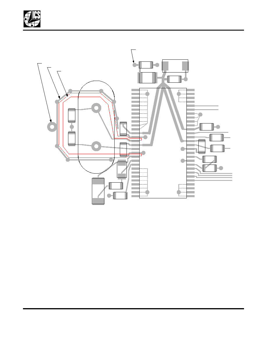
PCB Layout Recommendations
For optimum device performance and lowest output
phase noise, the following guidelines should be
observed. Please refer to the Recommended PCB
Layout drawing on the following page.
1) Each 0.01µF decoupling capacitor (CD) should be
mounted on the component side of the board as close
to the VDD pin as possible. No via's should be used
between the decoupling capacitor and VDD pin. The
PCB trace to VDD pin should be kept as short as
possible, as should the PCB trace to the ground via.
Distance of the ferrite chip and bulk decoupling from
the device is less critical.
2) The loop filter components must also be placed
close to the LF and LFR pins. C
P
should be closest to
the device. Coupling of noise from other system signal
traces should be minimized by keeping traces short
and away from active signal traces. Use of vias should
be avoided.
3) The external crystal should be mounted as close to
the device as possible, on the component side of the
board. This will help keep the crystal PCB traces short
to minimize parasitic load capacitance on the crystal
leads as well as noise pickup. The crystal traces should
be spaced away from each other and should use
minimum trace width. There should be no signal traces
near the crystal or the traces. Also refer to the Optional
Crystal Shielding section that follows.
4) To minimize EMI the 33
series termination resistor,
if needed, should be placed close to the clock output.
5) All components should be on the same side of the
board, minimizing vias through other signal layers (the
ferrite bead and bulk decoupling capacitor may be
mounted on the back). Other signal traces should be
routed away from the MK2069-03. This includes signal
traces on PCB traces just underneath the device, or on
layers adjacent to the ground plane layer used by the
device.
6) Because each input selection pin includes an
internal pull-up device, those inputs requiring a logic
high state ("1") can be left unconnected. The pins
requiring a logic low state ("0") can be grounded.
Optional Crystal Shielding
The crystal and connection traces to pins X1 and X2
are sensitive to noise pickup. In applications that are

VCXO-Based Clock Translator with High Multiplication
MDS 2069-03 I
12
Revision 050203
Integrated Circuit Systems, Inc.
l
525 Race Street, San Jose, CA 95126
l
tel (408) 295-9800
l
www.icst.com
MK2069-03
especially sensitive to noise, such as SONET or G-Bit
ethernet transceivers, some or all of the following
crystal shielding techniques should be considered. This
is especially important when the MK2069-03 is placed
near high speed logic or signal traces.
The following techniques are illustrated on the
Recommended PCB Layout drawing.
1) The metal layer underneath the crystal section
should be the ground layer. Remove all other layers
that are above. This ground layer will help shield the
crystal circuit from other system noise sources. As an
alternative, all layers underneath the crystal can be
removed, however this is not recommended if there are
adjacent PCBs that can induce noise into the
unshielded crystal circuit.
2) Cut a channel in the PCB ground plane around the
crystal area as shown. This will eliminate high
frequency ground currents that can couple into the
crystal circuit.
3) Add a through-hole for the optional third lead offered
by the crystal manufacturer (case ground). The
requirement for this third lead can be made at prototype
evaluation. The crystal is less sensitive to system noise
interference when the case is grounded.
4) Add a ground trace around the crystal circuit to
shield from other active traces on the component layer.
The external crystal is particularly sensitive to other
system clock sources that are at or near the crystal
frequency since it will try to lock to the interfering clock
source. The crystal should be keep away from these
clock sources.
The ICS Applications Note MAN05 may also be
referenced for additional suggestions on layout of the
crystal section.

VCXO-Based Clock Translator with High Multiplication
MDS 2069-03 I
13
Revision 050203
Integrated Circuit Systems, Inc.
l
525 Race Street, San Jose, CA 95126
l
tel (408) 295-9800
l
www.icst.com
MK2069-03
Recommended PCB Layout Diagram
Components are identified by function (top line) and by typical package type (bottom line) which may vary.
Legend:
G = Via to PCB Ground plane
V = Via to PCB Power Plane
CE = EMI suppression cap, typical value 0.1
µF
(ceramic)
FC = Ferrite chip
CBD = Bulk decoupling capacitor for chip power
supply, 1
µF minimum (tantalum)
CBB = Bulk bypass cap for chip power supply, typical
value 1000 pF (ceramic)
CD = Decoupling capacitor for VDD pin (ceramic)
CL = Optional load capacitor for crystal tuning (do not
stuff)
CS = External loop capacitor C
S
(film type)
CP = External loop capacitor C
P
(film type)
RS = External loop resistor R
S
RSET = Resistor RSET used to determine charge
pump current
RT = Series termination resistor for clock output,
typical value 33
RLD* = External resistor for lock detector circuit
CLD* = External capacitor for lock detector circuit
*Note: If output LD is not used, RLD and CLD may be
omitted. See text on page 10.
RSET
603
G
G
G
G
1
2
3
4
5
6
7
8
9
10
11
12
13
14
15
16
17
18
19
20
21
22
23
24
25
26
27
28
56
55
54
53
52
51
50
49
48
47
46
45
44
43
42
41
40
39
38
37
36
35
34
33
32
31
30
29
G
G
G
G
RS
603
RLD
603
RT
603
RT
603
CD
603
G
G
G
G
CD 603
CD 603
G
V
G
CS 1206
XTAL
CD 603
FC
A
CL 60
3
CL 603
SUPPLY SOURCE TO DEVICE
(SUCH AS VIA TO SUPPLY PLANE)
CE
603
CBB
603
CBD
A
G
G
G
G
G
G
G
G
OPTIONAL CRYSTAL SHIELDING
THRU HOLE FOR 3RD LEAD (XTAL CASE GROUND)
SHIELD TRACE (TOP LAYER)
CUT CHANNEL IN GROUND PLANE
MK2069
CP 805
CLD
603
G

VCXO-Based Clock Translator with High Multiplication
MDS 2069-03 I
14
Revision 050203
Integrated Circuit Systems, Inc.
l
525 Race Street, San Jose, CA 95126
l
tel (408) 295-9800
l
www.icst.com
MK2069-03
Circuit Troubleshooting
1) IF TCLK or VCLK does not lock to ICLK
First check VCLK to ICLK. It is best to display and
trigger the scope with RCLK, especially if a non-integer
VCXO PLL multiplication ratio is used.
If VCLK is not locked to ICLK:
1.1) Ensure the proper ICLK input is selected.
1.2) Check Divider settings.
1.3) Ensure ICLK is within lock range (within about 100
ppm of the nominal input frequency, limited by pull
range of the external crystal). If in doubt, tweak the
ICLK frequency up and down to see if VCLK locks.
1.4) Ensure ICLK jitter is not excessive. If ICLK jitter is
excessive device may not lock. Also see item 2.1
below.
1.5) Clean the PCB. The VCXO PLL loop filter is very
sensitive to board leakage, especially when the VCXO
PLL phase detector frequency is in the low kHz. If
organic solder flux is used (most common today) scrub
the PCB board with detergent and water and then blow
and bake dry. Inorganic solder flux (Rosen core)
requires solvent. See also section 3 below.
2) If There is Excessive Jitter on VCLK or
TCLK
2.1) The problem may be an unstable input reference
clock. An unstable ICLK will not appear to jitter when
ICLK is used as the oscilloscope trigger source. In this
condition, VCLK and TCLK may appear to be unstable
since the jitter from ICLK (the trigger source) has been
removed by the trigger circuit of the scope.
2.2) The instability may be caused by VCXO PLL loop
filter leakage. Refer to item 1.5 above.
2.3) VCLK and TCLK jitter can also be caused by poor
power supply decoupling. Ensure a bulk decoupling
capacitor is in place.
2.4) Ensure that the VCXO PLL loop bandwidth is
sufficiently low. It should be at least 1/20th of the phase
detector frequency.
2.5) Ensure that the VCXO PLL loop damping is
sufficient. If should be at least 0.7, preferably 1.0 or
higher.
2.6) Ensure that the 2nd pole in the VCXO PLL loop
filter is set sufficiently. In general, C
P
should be equal to
C
S
/20. If C
P
is too high, passband peaking will occur
and loop instability may occur. If C
P
is set too low,
excessive VCXO modulation by the charge correction
pulses may occur.
3) If There is Excessive Input to Output Skew
3.1) TCLK should track VCLK. The rising edge of TCLK
should be within a few nanoseconds of VCLK.
3.2) VCLK should track RCLK. The rising edge of
VCLK should be within 5-10 nsec of RCLK (VCLK
leads).
3.3) The biggest cause of input to output skew is VCXO
PLL loop filter leakage. Skew is best observed by
comparing ICLK to RCLK. When no leakage is present
the rising edge of RCLK should lag the rising edge of
ICLK by about 10
µsec. Loop filter leakage can greatly
increase this lag time or cause the loop to not lock.
Refer to item 1.5, above.
3.4) Another way to view the loop filter leakage is to
observe LDR pin. Use RCLK as the scope trigger. LDR
will produce a negative pulse equal in length to the
charge pump pulse.
3.5) Filter leakage can also be caused by the use of
improper loop capacitors. Refer to the section titled
`Loop Filter Capacitor Type' on page 8.

VCXO-Based Clock Translator with High Multiplication
MDS 2069-03 I
15
Revision 050203
Integrated Circuit Systems, Inc.
l
525 Race Street, San Jose, CA 95126
l
tel (408) 295-9800
l
www.icst.com
MK2069-03
Absolute Maximum Ratings
Stresses above the ratings listed below can cause permanent damage to the MK2069-03. These ratings,
which are standard values for ICS industrial rated parts, are stress ratings only. Functional operation of the
device at these or any other conditions above those indicated in the operational sections of the
specifications is not implied. Exposure to absolute maximum rating conditions for extended periods can
affect product reliability. Electrical parameters are guaranteed only over the recommended operating
temperature range.
Recommended Operation Conditions
Item
Rating
Supply Voltage, VDD
7V
All Inputs and Outputs
-0.5V to VDD+0.5V
Ambient Operating Temperature
-40 to +85
∞C
Storage Temperature
-65 to +150
∞C
Junction Temperature
175
∞C
Soldering Temperature
260
∞C
Parameter
Min.
Typ.
Max.
Units
Ambient Operating Temperature
-40
+85
∞C
Power Supply Voltage (measured in respect to GND)
+3.15
+3.3
+3.45
V

VCXO-Based Clock Translator with High Multiplication
MDS 2069-03 I
16
Revision 050203
Integrated Circuit Systems, Inc.
l
525 Race Street, San Jose, CA 95126
l
tel (408) 295-9800
l
www.icst.com
MK2069-03
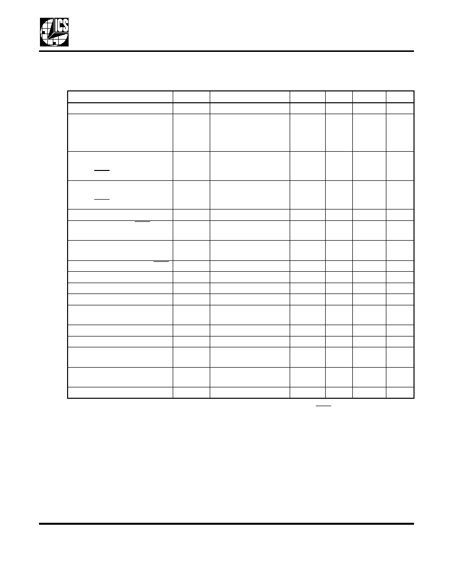
DC Electrical Characteristics
Unless stated otherwise, VDD = 3.3V ±5%, Ambient Temperature -40 to +85
∞C
Note 1: All logic select inputs (FV11:0, FPV5:0, SV2:0, FT5:0, RT1:0, ST1:0, CLR) have an internal pull-up
resistor.
Note 2: ICLK can safely be brought to V
IH
max prior to the application of VDD, providing utility in hot-plug
line card applications.
Parameter
Symbol
Conditions
Min.
Typ.
Max.
Units
Operating Voltage
VDD
3.15
3.3
3.45
V
Supply Current
IDD
All clock outputs
loaded with 15 pF,
VCLK = 19.44 MHz,
TCLK = 155.52 MHz
20
30
mA
Input High Voltage, FV11:0,
FPV5:0, SV2:0, FT5:0, RT1:0,
ST1:0, CLR
V
IH
2
VDD +
0.4
V
Input Low Voltage, FV11:0,
FPV5:0, SV2:0, FT5:0, RT1:0,
ST1:0, CLR
V
IL
-0.4
0.8
V
Input Pull-Up Resistor (Note 1)
R
PU
200
k
Input High Voltage, CLR
V
IH
VDD/2+1
VDD +
0.4
V
Input High Voltage, ICLK
(Note 2)
V
IH
VDD/2+1
5.5
V
Input Low Voltage, ICLK, CLR
V
IL
-0.4
VDD/2-1
V
Input High Current (Note 1)
I
IH
V
IH
= VDD
-10
+10
µA
Input Low Current (Note 1)
I
IL
V
IL
= 0
-10
+10
µA
Input Capacitance, except X1
C
IN
7
pF
Output High Voltage
(CMOS Level)
V
OH
I
OH
= -4 mA
VDD-0.4
V
Output High Voltage
V
OH
I
OH
= -8 mA
2.4
V
Output Low Voltage
V
OL
I
OL
= 4 mA
0.4
V
Output Short Circuit Current,
TCLK
I
OS
±50
mA
Output Short Circuit Current,
VCLK, RCLK and LD
I
OS
±20
mA
VIN, VCXO Control Voltage
V
XC
0
VDD
V

VCXO-Based Clock Translator with High Multiplication
MDS 2069-03 I
17
Revision 050203
Integrated Circuit Systems, Inc.
l
525 Race Street, San Jose, CA 95126
l
tel (408) 295-9800
l
www.icst.com
MK2069-03
AC Electrical Characteristics
Unless stated otherwise, VDD = 3.3V ±5%, Ambient Temperature -40 to +85
∞ C
Parameter
Symbol
Conditions
Min.
Typ.
Max. Units
Crystal Frequency Range
(Note 1)
f
XTAL
Using recommended
crystal
13.5
27
MHz
VCXO Crystal Pull Range
f
XP
Using recommended
crystal
±115
±150
ppm
VCXO Crystal Free-Run
Frequency (Note 2)
f
XF
Input reference = 0 Hz
-300
-150
ppm
Input Clock Frequency (Note 3)
f
I
0.001
27
MHz
Input Clock Pulse Width
t
ID
Positive or Negative
Pulse
10
nsec
VCXO PLL Phase Detector Jitter
Tolerance
t
JT
1 UI = phase detector
period
0.4
UI
Translator PLL VCO Frequency
f
V
40
320
MHz
Timing Jitter, Filtered
500Hz-1.3MHz (OC-3)
t
OJf
Derived from phase
noise characteristics,
peak-to-peak 6 sigma
95
ps
Timing Jitter, Filtered
65kHz-5MHz (OC-3)
t
OJf
Derived from phase
noise characteristics,
peak-to-peak 6 sigma
85
ps
Timing Jitter, Filtered
1kHz-5MHz (OC-12)
t
OJf
Derived from phase
noise characteristics,
peak-to-peak 6 sigma
105
ps
Timing Jitter, Filtered
250kHz-5MHz (OC-12)
t
OJf
Derived from phase
noise characteristics,
peak-to-peak 6 sigma
80
ps
Output Frequency
VCO frequency = 40 to
320 MHz
2.5
160
MHz
Output Duty Cycle (% high time),
VCLK when SV Divider = 1
t
OD
Measured at VDD/2,
C
L
=15pF
40
50
60
%
Output Duty Cycle (% high time),
VCLK when SV Divider > 1,
TCLK
t
OD
Measured at VDD/2,
C
L
=15pF
44
50
65
%
Output High Time, RCLK
(Note 4)
t
OH
Measured at VDD/2,
C
L
=15pF
0.5
VCLK
Period
Output Rise Time, VCLK and
RCLK
t
OR
0.8 to 2.0V, C
L
=15pF
1.5
2
ns
Output Fall Time, VCLK and
RCLK
t
OF
2.0 to 0.8V, C
L
=15pF
1.5
2
ns

VCXO-Based Clock Translator with High Multiplication
MDS 2069-03 I
18
Revision 050203
Integrated Circuit Systems, Inc.
l
525 Race Street, San Jose, CA 95126
l
tel (408) 295-9800
l
www.icst.com
MK2069-03
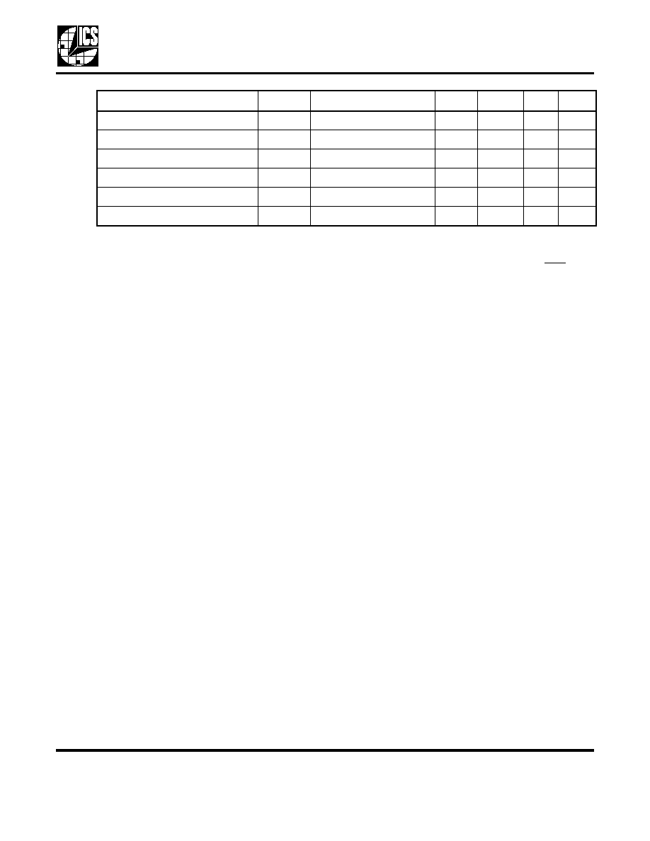
Note 1: This is the recommended crystal operating range. A crystal as low as 8 MHz can be used, although
this may result in increased output phase noise.
Note 2: The VCXO crystal will be pulled to its minimum frequency when there is no input clock (CLR = 1)
due to the attempt of the PLL to lock to 0 Hz.
Note 3: The minimum practical phase detector frequency is is assumed to be 1 kHz. Through proper loop
filter design lower input frequencies may be possible. Input frequencies as low as 400Hz have been
implemented.
Note 4: The output of RCLK is a positive pulse with a duration equal to VCLK high time, or half the VCLK
period.
Note 5: Referenced to ICLK, the skews of VCLK, RCLK and TCLK increase together when leakage is
present in the external VCXO PLL loop filter.
Output Rise Time, TCLK
t
OR
0.8 to 2.0V, C
L
=15pF
0.75
1
ns
Output Fall Time, TCLK
t
OF
2.0 to 0.8V, C
L
=15pF
0.75
1
ns
Skew, ICLK to VCLK (Note 5)
t
IV
Rising edges, C
L
=15pF
-5
2.5
+10
ns
Skew, ICLK to RCLK (Note 5)
t
IV
Rising edges, C
L
=15pF
+5
10
+20
ns
Skew, ICLK to TCLK (Note 5)
t
VT
Rising edges, C
L
=15pF
-5
1.5
+10
ns
Nominal Output Impedance
Z
OUT
20
Parameter
Symbol
Conditions
Min.
Typ.
Max. Units

VCXO-Based Clock Translator with High Multiplication
MDS 2069-03 I
19
Revision 050203
Integrated Circuit Systems, Inc.
l
525 Race Street, San Jose, CA 95126
l
tel (408) 295-9800
l
www.icst.com
MK2069-03
Package Outline and Package Dimensions
56 pin TSSOP
6.10 mm (240 mil) body, 0.50 mm. (20 mil) pitch
Package dimensions are kept current with JEDEC Publication No. 95
Ordering Information
While the information presented herein has been checked for both accuracy and reliability, Integrated Circuit Systems (ICS)
assumes no responsibility for either its use or for the infringement of any patents or other rights of third parties, which would
result from its use. No other circuits, patents, or licenses are implied. This product is intended for use in normal commercial
applications. Any other applications such as those requiring extended temperature range, high reliability, or other extraordinary
environmental requirements are not recommended without additional processing by ICS. ICS reserves the right to change any
circuitry or specifications without notice. ICS does not authorize or warrant any ICS product for use in life support devices or
critical medical instruments.
Part / Order Number
Marking
Shipping
packaging
Package
Temperature
MK2069-03GI
MK2069-03GI
Tubes
56 pin TSSOP
-40 to +85
∞ C
MK2069-03GITR
MK2069-03GI
Tape and Reel
56 pin TSSOP
-40 to +85
∞ C
IN D E X
A R E A
1 2
56
D
E 1
E
S E A T IN G
P LA N E
A
1
A
A
2
e
- C -
b
aaa
C
c
L
Millimeters
Inches
Symbol
Min
Max
Min
Max
A
--
1.20
--
0.047
A1
0.05
0.15
0.002
0.006
A2
0.80
1.05
0.032
0.041
b
0.17
0.27
0.007
0.011
C
0.09
0.20
0.0035
0.008
D
13.90
14.10
0.547
0.555
E
8.10 BASIC
0.319 BASIC
E1
6.00
6.20
0.236
0.244
e
0.50 Basic
0.020 Basic
L
0.45
0.75
0.018
0.030
0
∞
8
∞
0
∞
8
∞
aaa
--
0.10
--
0.004
