Äîêóìåíòàöèÿ è îïèñàíèÿ www.docs.chipfind.ru
Integrated
Circuit
Systems, Inc.
ICS9248-99
Third party brands and names are the property of their respective owners.
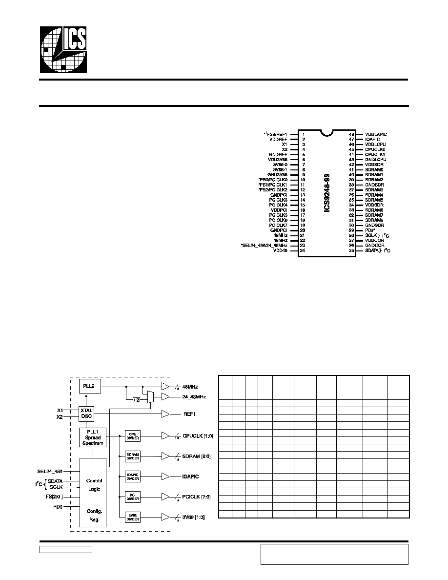
Block Diagram
9248- 99 Rev A 8/27/99
Recommended Application:
810/810E style chipset
Output Features:
·
2- CPUs @2.5V @ 150MHz (up to 200MHz. achievable
through I
2
C)
·
9 - SDRAM @ 3.3V @ 150MHz (up to 200MHz.
achievable through I
2
C)
·
8 - PCICLK @ 3.3V
·
1 - IOAPIC @ 2.5V,
·
2 - 3V66MHz @ 3.3V
·
2- 48MHz, @ 3.3V fixed.
·
1- 24/48MHz, @ 3.3V
·
1- REF @3.3V, 14.318MHz.
Features:
·
Up to 200.4MHz frequency support
·
Support FS0-FS3 trapping status bit for I
2
C read back.
·
Support power management: Power down Mode form I
2
C
programming.
·
Spread spectrum for EMI control ( ± 0.25% center).
·
FS0, FS1, FS2, FS3 must have a internal 120K pull-Down
to GND.
·
Uses external 14.318MHz crystal
Skew Specifications:
·
CPU CPU: <175ps
·
SDRAM - SDRAM: < 250ps
·
3V66 3V66: <175ps
·
PCI PCI: <500ps
·
For group skew specifications, please refer to group
timing relationship table.
Functionality
3
S
F
2
S
F
1
S
F
0
S
F
U
P
C
)
z
H
M
(
M
A
R
D
S
)
z
H
M
(
6
6
V
3
)
z
H
M
(
K
L
C
I
C
P
*
6
6
V
3
(
)
2
/
1
)
z
H
M
(
C
I
P
A
O
I
*
I
C
P
(
)
2
/
1
)
z
H
M
(
C
I
P
A
O
I
)
I
C
P
(
)
z
H
M
(
0
0
0
0
3
3
.
5
7
0
0
.
3
1
1
3
3
.
5
7
7
6
.
7
3
3
8
.
8
1
7
6
.
7
3
0
0
0
1
0
0
.
5
2
1
0
0
.
5
2
1
3
3
.
3
8
7
6
.
1
4
3
8
.
0
2
7
6
.
1
4
0
0
1
0
0
0
.
9
2
1
0
0
.
9
2
1
0
0
.
6
8
0
0
.
3
4
0
5
.
1
2
0
0
.
3
4
0
0
1
1
9
2
.
0
5
1
0
0
.
3
1
1
3
3
.
5
7
7
6
.
7
3
3
8
.
8
1
7
6
.
7
3
0
1
0
0
0
0
.
0
5
1
0
0
.
0
5
1
0
0
.
0
0
1
0
0
.
0
5
0
0
.
5
2
0
0
.
0
5
0
1
0
1
0
0
.
2
1
1
0
0
.
2
1
1
7
6
.
4
7
3
3
.
7
3
7
6
.
8
1
3
3
.
7
3
0
1
1
0
0
0
.
5
4
1
0
0
.
5
4
1
7
6
.
6
9
3
3
.
8
4
7
1
.
4
2
3
3
.
8
4
0
1
1
1
4
6
.
3
4
1
0
0
.
8
0
1
0
0
.
2
7
0
0
.
6
3
0
0
.
8
1
0
0
.
6
3
1
0
0
0
0
3
.
8
6
0
5
.
2
0
1
3
3
.
8
6
7
1
.
4
3
8
0
.
7
1
7
1
.
4
3
1
0
0
1
0
0
.
5
0
1
0
0
.
5
0
1
0
0
.
0
7
0
0
.
5
3
0
5
.
7
1
0
0
.
5
3
1
0
1
0
0
0
.
8
3
1
0
0
.
8
3
1
0
0
.
2
9
0
0
.
6
4
0
0
.
3
2
0
0
.
6
4
1
0
1
1
0
0
.
0
4
1
0
0
.
5
0
1
0
0
.
0
7
0
0
.
5
3
0
5
.
7
1
0
0
.
5
3
1
1
0
0
7
6
.
6
6
0
0
.
0
0
1
7
6
.
6
6
3
3
.
3
3
7
6
.
6
1
3
3
.
3
3
1
1
0
1
0
0
.
0
0
1
0
0
.
0
0
1
7
6
.
6
6
3
3
.
3
3
7
6
.
6
1
3
3
.
3
3
1
1
1
0
0
6
.
3
3
1
0
6
.
3
3
1
7
0
.
9
8
3
5
.
4
4
7
2
.
2
2
3
5
.
4
4
1
1
1
1
3
3
.
3
3
1
0
0
.
0
0
1
7
6
.
6
6
3
3
.
3
3
7
6
.
6
1
3
3
.
3
3
Pin Configuration
48-Pin 300mil SSOP
* These inputs have a 120K pull down to GND.
1 These are double strength.
Frequency Generator & Integrated Buffers for Celeron & P
II
/
III
TM
Preliminary Product Preview
PRODUCT PREVIEW documents contain information on new
products in the sampling or preproduction phase of development.
Characteristic data and other specifications are subject to change
without notice.
2
ICS9248-99
Preliminary Product Preview
Third party brands and names are the property of their respective owners.
General Description
Pin Configuration
The ICS9248-99 is the single chip clock solution for Desktop
designs using 810/810/E style chipset. It provides all necessary
clock signals for such a system.
Spread spectrum may be enabled through I
2
C programming.
Spread spectrum typically reduces system EMI by 8dB to
10dB. This simplifies EMI qualification without resorting to
board design iterations or costly shielding. The ICS9248-99
employs a proprietary closed loop design, which tightly
controls the percentage of spreading over process and
temperature variations.
Serial programming I
2
C interface allows changing functions,
stop clock programming and frequency selection.
Power Groups
GNDREF, VDDREF = REF1, X1, X2
GNDPCI , VDDPCI = PCICLK [7:0]
GNDSDR, VDDSDR = SDRAM [8:0]
GNDCOR, VDDCOR = supply for PLL core
GND3V66 , VDD3V66 = 3V66
VDD48 = 48MHz, 24_48MHz,
VDDLAPIC = IOAPIC
GNDLCPU , VDDLCPU = CPUCLK [1:0]
PIN NUMBER
PIN NAME
TYPE
DESCRIPTION
REF1
OUT
14.318 MHz reference clock.
FS3
IN
Frequency select pin.
2, 6, 16, 24, 27, 34,
42
VDD
PWR
3.3V Power supply for SDRAM output buffers, PCI output buffers,
reference output buffers and 48MHz output
3
X1
IN
Crystal input,nominally 14.318MHz.
4
X2
OUT
Crystal output, nominally 14.318MHz.
5, 9, 13, 20, 26, 30,
38
GND
PWR
Ground pin for 3V outputs.
8, 7
3V66 [1:0]
OUT
3.3V clock outputs
FS0
IN
Frequency select pin.
PCICLK0
OUT
PCI clock output.
FS1
IN
Frequency select pin.
PCICLK1
OUT
PCI clock output.
FS2
IN
Frequency select pin.
PCICLK2
OUT
PCI clock output.
19, 18, 17, 15, 14
PCICLK [7:3]
OUT
PCI clock outputs.
21, 22
48MHz
OUT
48MHz output clocks
SEL24_48#
IN
Select pin for enabling 24MHz or 48MHz
H=24MHz L=48MHz
24_48MHz
OUT
Clock output for super I/O/USB
25
SDATA
IN
Data input for I2C serial input, 5V tolerant input
28
SCLK
IN
Clock input of I2C input, 5V tolerant input
29
PD#
IN
Asynchronous active low input pin used to power down the device into a low
power state. The internal clocks are disabled and the VCO and the crystal are
stopped. The latency of the power down will not be greater than 3ms.
31, 32, 33, 35, 36,
37, 39, 40, 41
SDRAM [8:0]
OUT
SDRAM clock outputs
43
GNDLCPU
PWR
Ground pin for the CPU clocks.
44, 45
CPUCLK [1:0]
OUT
CPU clock outputs.
46
VDDLCPU
PWR
Power pin for the CPUCLKs. 2.5V
47
IOAPIC
OUT
2.5V clock output.
48
VDDLAPIC
PWR
Power pin for the IOAPIC. 2.5V
23
1
11
12
10
3
ICS9248-99
Preliminary Product Preview
Third party brands and names are the property of their respective owners.
1.
The ICS clock generator is a slave/receiver, I
2
C component. It can read back the data stored in the latches for
verification. Read-Back will support Intel PIIX4 "Block-Read" protocol.
2.
The data transfer rate supported by this clock generator is 100K bits/sec or less (standard mode)
3.
The input is operating at 3.3V logic levels.
4.
The data byte format is 8 bit bytes.
5.
To simplify the clock generator I
2
C interface, the protocol is set to use only "Block-Writes" from the controller. The
bytes must be accessed in sequential order from lowest to highest byte with the ability to stop after any complete byte
has been transferred. The Command code and Byte count shown above must be sent, but the data is ignored for those
two bytes. The data is loaded until a Stop sequence is issued.
6.
At power-on, all registers are set to a default condition, as shown.
General I
2
C serial interface information
The information in this section assumes familiarity with I
2
C programming.
For more information, contact ICS for an I
2
C programming application note.
How to Write:
Controller (host) sends a start bit.
Controller (host) sends the write address D2
(H)
ICS clock will acknowledge
Controller (host) sends a dummy command code
ICS clock will acknowledge
Controller (host) sends a dummy byte count
ICS clock will acknowledge
Controller (host) starts sending first byte (Byte 0)
through byte 5
ICS clock will acknowledge each byte one at a time.
Controller (host) sends a Stop bit
How to Read:
Controller (host) will send start bit.
Controller (host) sends the read address D3
(H)
ICS clock will acknowledge
ICS clock will send the byte count
Controller (host) acknowledges
ICS clock sends first byte (Byte 0) through byte 5
Controller (host) will need to acknowledge each byte
Controller (host) will send a stop bit
Notes:
Controller (Host)
ICS (Slave/Receiver)
Start Bit
Address
D3
(H)
ACK
Byte Count
ACK
Byte 0
ACK
Byte 1
ACK
Byte 2
ACK
Byte 3
ACK
Byte 4
ACK
Byte 5
ACK
Stop Bit
How to Read:
Controller (Host)
ICS (Slave/Receiver)
Start Bit
Address
D2
(H)
ACK
Dummy Command Code
ACK
Dummy Byte Count
ACK
Byte 0
ACK
Byte 1
ACK
Byte 2
ACK
Byte 3
ACK
Byte 4
ACK
Byte 5
ACK
Stop Bit
How to Write:
4
ICS9248-99
Preliminary Product Preview
Third party brands and names are the property of their respective owners.
Byte4: Functionality and Frequency Select Register (default = 0)
Serial Configuration Command Bitmap
Note 1: Default at power-up will be for latched logic inputs to define frequency, as displayed by Bit 3.
1) The IOAPIC Frequency change from IOAPIC=PCICLK/2 to IOAPIC=PCICLK is controlled by
IOAPC_Freq control in
I
2
C
Byte 3 Bit 1
2) The I
2
C readback of the power up default indicate the revision ID in bits 2, 7:4
I
2
C is a trademark of Philips Corporation
t
i
B
n
o
i
t
p
i
r
c
s
e
D
D
W
P
,
2
t
i
B
4
:
7
t
i
B
)
4
:
7
,
2
(
t
i
B
K
L
C
U
P
C
)
z
H
M
(
M
A
R
D
S
)
z
H
M
(
6
6
V
3
)
z
H
M
(
K
L
C
I
C
P
z
H
M
(
C
I
P
A
O
I
)
z
H
M
(
1
1
0
0
0
1
e
t
o
N
2
/
I
C
P
=
I
C
P
=
0
0
0
0
0
3
3
.
5
7
0
0
.
3
1
1
3
3
.
5
7
7
6
.
7
3
3
8
.
8
1
7
6
.
7
3
0
0
0
0
1
0
0
.
5
2
1
0
0
.
5
2
1
3
3
.
3
8
7
6
.
1
4
3
8
.
0
2
7
6
.
1
4
0
0
0
1
0
0
0
.
9
2
1
0
0
.
9
2
1
0
0
.
6
8
0
0
.
3
4
0
5
.
1
2
0
0
.
3
4
0
0
0
1
1
9
2
.
0
5
1
0
0
.
3
1
1
3
3
.
5
7
7
6
.
7
3
3
8
.
8
1
7
6
.
7
3
0
0
1
0
0
0
0
.
0
5
1
0
0
.
0
5
1
0
0
.
0
0
1
0
0
.
0
5
0
0
.
5
2
0
0
.
0
5
0
0
1
0
1
0
0
.
2
1
1
0
0
.
2
1
1
7
6
.
4
7
3
3
.
7
3
7
6
.
8
1
3
3
.
7
3
0
0
1
1
0
0
0
.
5
4
1
0
0
.
5
4
1
7
6
.
6
9
3
3
.
8
4
7
1
.
4
2
3
3
.
8
4
0
0
1
1
1
4
6
.
3
4
1
0
0
.
8
0
1
0
0
.
2
7
0
0
.
6
3
0
0
.
8
1
0
0
.
6
3
0
1
0
0
0
0
3
.
8
6
0
5
.
2
0
1
3
3
.
8
6
7
1
.
4
3
8
0
.
7
1
7
1
.
4
3
0
1
0
0
1
0
0
.
5
0
1
0
0
.
5
0
1
0
0
.
0
7
0
0
.
5
3
0
5
.
7
1
0
0
.
5
3
0
1
0
1
0
0
0
.
8
3
1
0
0
.
8
3
1
0
0
.
2
9
0
0
.
6
4
0
0
.
3
2
0
0
.
6
4
0
1
0
1
1
0
0
.
0
4
1
0
0
.
5
0
1
0
0
.
0
7
0
0
.
5
3
0
5
.
7
1
0
0
.
5
3
0
1
1
0
0
7
6
.
6
6
0
0
.
0
0
1
7
6
.
6
6
3
3
.
3
3
7
6
.
6
1
3
3
.
3
3
0
1
1
0
1
0
0
.
0
0
1
0
0
.
0
0
1
7
6
.
6
6
3
3
.
3
3
7
6
.
6
1
3
3
.
3
3
0
1
1
1
0
0
6
.
3
3
1
0
6
.
3
3
1
7
0
.
9
8
3
5
.
4
4
7
2
.
2
2
3
5
.
4
4
0
1
1
1
1
3
3
.
3
3
1
0
0
.
0
0
1
7
6
.
6
6
3
3
.
3
3
7
6
.
6
1
3
3
.
3
3
1
0
0
0
0
4
9
.
6
5
1
0
0
.
8
1
1
7
6
.
8
7
3
3
.
9
3
7
6
.
9
1
3
3
.
9
3
1
0
0
0
1
0
0
.
0
6
1
0
0
.
0
2
1
0
0
.
0
8
0
0
.
0
4
0
0
.
0
2
0
0
.
0
4
1
0
0
1
0
0
3
.
6
4
1
0
0
.
0
1
1
3
3
.
3
7
7
6
.
6
3
3
3
.
8
1
7
6
.
6
3
1
0
0
1
1
0
0
.
7
2
1
5
2
.
5
9
0
5
.
3
6
5
7
.
1
3
8
8
.
5
1
5
7
.
1
3
1
0
1
0
0
0
0
.
7
2
1
0
0
.
7
2
1
7
6
.
4
8
3
3
.
2
4
7
1
.
1
2
3
3
.
2
4
1
0
1
0
1
0
0
.
1
2
1
0
0
.
1
2
1
7
6
.
0
8
3
3
.
0
4
7
1
.
0
2
3
3
.
0
4
1
0
1
1
0
0
0
.
7
1
1
0
0
.
7
1
1
0
0
.
8
7
0
0
.
9
3
0
5
.
9
1
0
0
.
9
3
1
0
1
1
1
0
0
.
4
1
1
0
0
.
4
1
1
0
0
.
6
7
0
0
.
8
3
0
0
.
9
1
0
0
.
8
3
1
1
0
0
0
0
0
.
0
8
0
0
.
0
2
1
0
0
.
0
8
0
0
.
0
4
0
0
.
0
2
0
0
.
0
4
1
1
0
0
1
0
0
.
8
7
0
0
.
7
1
1
0
0
.
8
7
0
0
.
9
3
0
5
.
9
1
0
0
.
9
3
1
1
0
1
0
0
0
.
0
0
2
0
0
.
0
0
2
3
3
.
3
3
1
7
6
.
6
6
3
3
.
3
3
7
6
.
6
6
1
1
0
1
1
0
0
.
0
8
1
0
0
.
0
8
1
0
0
.
0
2
1
0
0
.
0
6
0
0
.
0
3
0
0
.
0
6
1
1
1
0
0
0
0
.
6
6
1
0
0
.
6
6
1
7
6
.
0
1
1
3
3
.
5
5
7
6
.
7
2
3
3
.
5
5
1
1
1
0
1
0
0
.
0
1
1
0
0
.
0
1
1
3
3
.
3
7
7
6
.
6
3
3
3
.
8
1
7
6
.
6
3
1
1
1
1
0
0
0
.
7
0
1
0
0
.
7
0
1
3
3
.
1
7
7
6
.
5
3
3
8
.
7
1
7
6
.
5
3
1
1
1
1
1
0
0
.
0
9
0
0
.
0
9
0
0
.
0
6
0
0
.
0
3
0
0
.
5
1
0
0
.
0
3
3
t
i
B
s
t
u
p
n
I
d
e
h
c
t
a
L
,
t
c
e
l
e
s
e
r
a
w
d
r
a
h
y
b
d
e
t
c
e
l
e
s
s
i
y
c
n
e
u
q
e
r
F
-
0
4
:
7
,
2
t
i
B
y
b
d
e
t
c
e
l
e
s
s
i
y
c
n
e
u
q
e
r
F
-
1
0
1
t
i
B
l
a
m
r
o
N
-
0
d
a
e
r
p
S
r
e
t
n
e
C
%
5
2
.
0
±
d
e
l
b
a
n
E
m
u
r
t
c
e
p
S
d
a
e
r
p
S
-
1
1
0
t
i
B
g
n
i
n
n
u
R
-
0
s
t
u
p
t
u
o
l
l
a
e
t
a
t
s
i
r
T
-
1
0
5
ICS9248-99
Preliminary Product Preview
Third party brands and names are the property of their respective owners.
Byte 0: CPU, Active/Inactive Register
(1= enable, 0 = disable)
T
I
B
#
N
I
P
D
W
P
N
O
I
T
P
I
R
C
S
E
D
7
t
i
B
-
0
d
e
v
r
e
s
e
R
6
t
i
B
-
0
d
e
v
r
e
s
e
R
5
t
i
B
-
0
d
e
v
r
e
s
e
R
4
t
i
B
-
0
d
e
v
r
e
s
e
R
3
t
i
B
-
0
d
e
v
r
e
s
e
R
2
t
i
B
3
2
1
z
H
M
8
4
/
4
2
1
t
i
B
2
2
,
1
2
1
z
H
M
8
4
0
t
i
B
-
0
d
e
v
r
e
s
e
R
Notes:
1. Inactive means outputs are held LOW and are disabled
from switching.
2. Latched Frequency Selects (FS#) will be inferted logic
load of the input frequency select pin conditions.
Byte 3: Reserved , Active/Inactive Register
(1= enable, 0 = disable)
Byte 5: Peripheral , Active/Inactive Register
(1= enable, 0 = disable)
T
I
B
#
N
I
P
D
W
P
N
O
I
T
P
I
R
C
S
E
D
7
t
i
B
-
0
d
e
v
r
e
s
e
R
6
t
i
B
-
0
d
e
v
r
e
s
e
R
5
t
i
B
-
0
d
e
v
r
e
s
e
R
4
t
i
B
-
0
d
e
v
r
e
s
e
R
3
t
i
B
-
0
d
e
v
r
e
s
e
R
2
t
i
B
-
0
d
e
v
r
e
s
e
R
1
t
i
B
-
0
d
e
v
r
e
s
e
R
0
t
i
B
-
0
d
e
v
r
e
s
e
R
T
I
B
#
N
I
P
D
W
P
N
O
I
T
P
I
R
C
S
E
D
7
t
i
B
-
0
)
e
t
o
N
(
d
e
v
r
e
s
e
R
6
t
i
B
-
0
)
e
t
o
N
(
d
e
v
r
e
s
e
R
5
t
i
B
-
0
)
e
t
o
N
(
d
e
v
r
e
s
e
R
4
t
i
B
-
0
)
e
t
o
N
(
d
e
v
r
e
s
e
R
3
t
i
B
-
0
)
e
t
o
N
(
d
e
v
r
e
s
e
R
2
t
i
B
-
1
)
e
t
o
N
(
d
e
v
r
e
s
e
R
1
t
i
B
-
1
)
e
t
o
N
(
d
e
v
r
e
s
e
R
0
t
i
B
-
0
)
e
t
o
N
(
d
e
v
r
e
s
e
R
Byte 6: Peripheral , Active/Inactive Register
(1= enable, 0 = disable)
Note: Dont write into this register, writing into this
register can cause malfunction
Byte 2: PCI, Active/Inactive Register
(1= enable, 0 = disable)
T
I
B
#
N
I
P
D
W
P
N
O
I
T
P
I
R
C
S
E
D
7
t
i
B
9
1
1
7
K
L
C
I
C
P
6
t
i
B
8
1
1
6
K
L
C
I
C
P
5
t
i
B
7
1
1
5
K
L
C
I
C
P
4
t
i
B
5
1
1
4
K
L
C
I
C
P
3
t
i
B
4
1
1
3
K
L
C
I
C
P
2
t
i
B
2
1
1
2
K
L
C
I
C
P
1
t
i
B
1
1
1
1
K
L
C
I
C
P
0
t
i
B
0
1
1
0
K
L
C
I
C
P
Byte 1: SDRAM, Active/Inactive Register
(1= enable, 0 = disable)
T
I
B
#
N
I
P
D
W
P
N
O
I
T
P
I
R
C
S
E
D
7
t
i
B
2
3
1
7
M
A
R
D
S
6
t
i
B
3
3
1
6
M
A
R
D
S
5
t
i
B
5
3
1
5
M
A
R
D
S
4
t
i
B
6
3
1
4
M
A
R
D
S
3
t
i
B
7
3
1
3
M
A
R
D
S
2
t
i
B
9
3
1
2
M
A
R
D
S
1
t
i
B
0
4
1
1
M
A
R
D
S
0
t
i
B
1
4
1
0
M
A
R
D
S
T
I
B
#
N
I
P
D
W
P
N
O
I
T
P
I
R
C
S
E
D
7
t
i
B
-
0
d
e
v
r
e
s
e
R
6
t
i
B
-
X
#
2
S
F
5
t
i
B
-
X
#
1
S
F
4
t
i
B
-
X
#
0
S
F
3
t
i
B
7
4
1
C
I
P
A
O
I
2
t
i
B
-
X
#
)
#
8
4
_
4
2
L
E
S
(
1
t
i
B
-
1
C
I
P
A
O
I
_
Q
E
R
F
2
/
K
L
C
I
C
P
=
C
I
P
A
O
I
>
=
1
=
>
=
0
=
C
I
P
A
O
I
_
Q
E
R
F
K
L
C
I
C
P
=
C
I
P
A
O
I
0
t
i
B
-
X
#
3
S
F