Äîêóìåíòàöèÿ è îïèñàíèÿ www.docs.chipfind.ru
Integrated
Circuit
Systems, Inc.
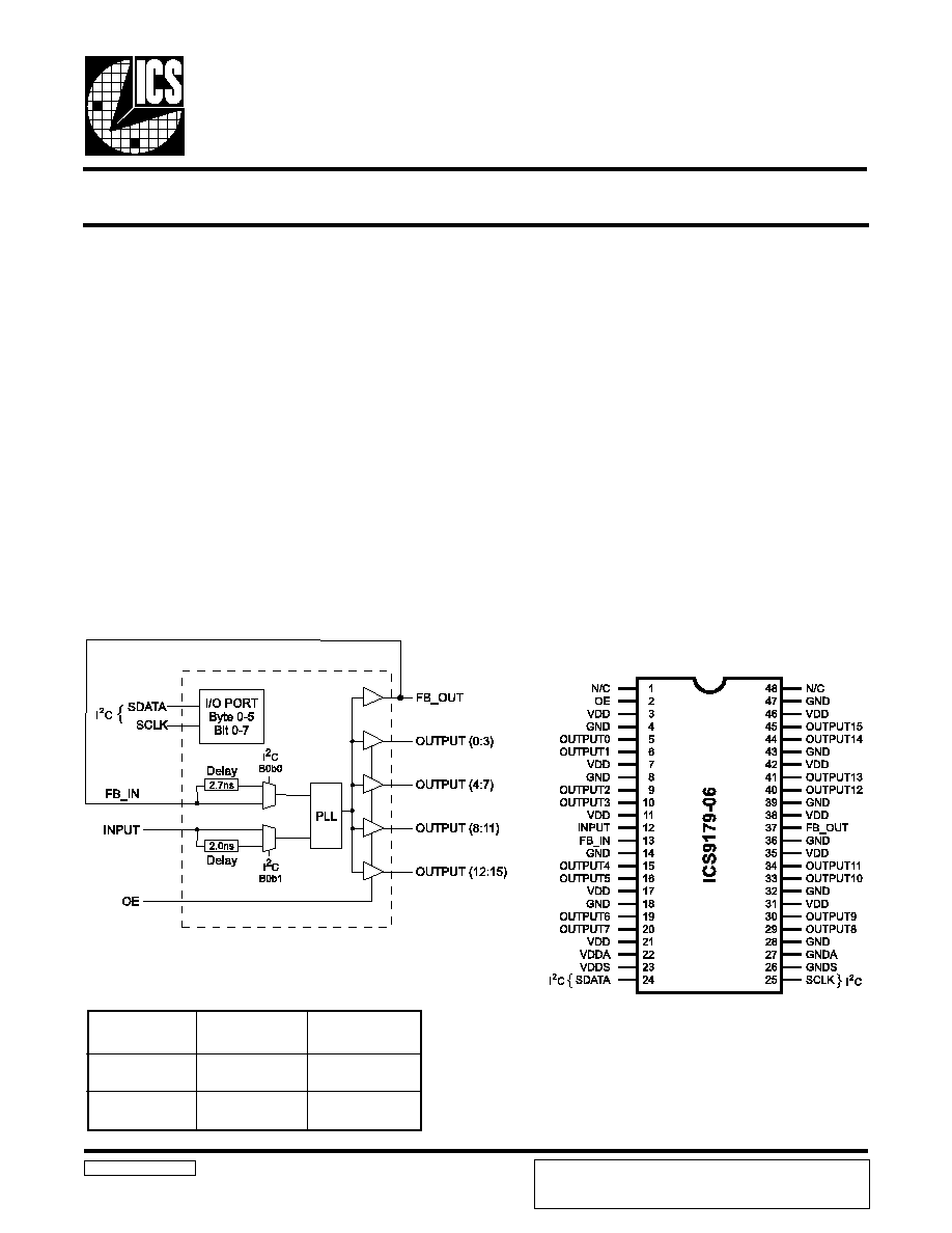
General Description
Features
ICS9179-06
Block Diagram
PentiumPro is a trademark of Intel Corporation
I
2
C is a trademark of Philips Corporation
Zero Delay Buffers
9179-06 Rev F 6/22/99
Pin Configuration
The ICS9179-06 generates low skew clock buffers required
for high speed RISC or CISC microprocessor systems such as
Intel PentiumPro. An output enable is provided for testability.
The device is a buffer with low output to output skew. This is
a zero delay buffer device, using an internal PLL. This buffer
can be used for phase synchronization to a master clock. With
the wide PLL loop BW, this buffer is compatible to Spread
Spectrum input clocks from clock generator products such as
the ICS9148-27.
The individual clock outputs are addressable through I
2
C to be
enabled, or stopped in a low state for reduced EMI when the
lines are not needed. The device defaults to zero-delay mode,
but can be programmed with I
2
C for selectable delays -2.7,
+2.0, -0.7 ns (nominal target values).
Zero delay buffer, 16 outputs
Supports up to four SDRAM DIMMS
Wide PLL loop bandwidth makes this part ideal in
Spread Spectrum applications.
Skew Input to FB_IN ±250ps default, with selectable
skew -2.7, +2.0, -0.7ns nominal.
Synchronous clocks skew matched to 250ps window on
output.
33 to 133MHz input or output frequency.
I
2
C Serial Configuration interface to allow individual
clocks to be stopped, or selectable delays.
Multiple VDD, VSS pins for noise reduction
Slew rate 1.5V/ns into 30pF.
VDD = 3.3 ±5%, 0 to 70°C
All outputs (0:15) tristate with OE low
(FB_OUT stays running).
48-Pin SSOP package
48-Pin SSOP
ICS reserves the right to make changes in the device data identified in
this publication without further notice. ICS advises its customers to
obtain the latest version of all device data to verify that any
information being relied upon by the customer is current and accurate.
Functionality
#
E
O
T
U
P
T
U
O
)
5
1
:
0
(
T
U
O
_
B
F
0
Z
-
i
H
T
U
P
N
I
X
1
1
T
U
P
N
I
X
1
T
U
P
N
I
X
1
2
ICS9179-06
Pin Descriptions
Power Groups
VDD = Power supply for OUTPUT buffers
VDDS = Power supply for I
2
C circuitry
VDDA = Power supply for Analog PLL circuitry
Notes:
1.
At power up all sixteen outputs are enabled and active.
2.
OE has a 100K Ohm internal pull-up resistor to keep all outputs active.
3.
The SDATA and SCLK inputs both also have internal pull-up resistors with values above 100K Ohms as well for
complete platform flexibility.
4.
I
2
C Byte0, bits 0 & 1 used to select delay. Default* values at power up is 0
5.
Subject to design engineering verification of target value.
R
E
B
M
U
N
N
I
P
E
M
A
N
N
I
P
E
P
Y
T
N
O
I
T
P
I
R
C
S
E
D
2
E
O
N
I
l
a
n
r
e
t
n
i
s
a
H
.
W
O
L
d
l
e
h
n
e
h
w
T
U
O
_
B
F
t
p
e
c
x
e
s
t
u
p
t
u
o
l
l
a
s
e
t
a
t
s
-
i
r
T
.
p
u
-
l
l
u
p
2
0
1
,
9
,
6
,
5
)
3
:
0
(
T
U
P
T
U
O
T
U
O
s
t
u
p
t
u
o
k
c
o
l
c
0
e
t
y
B
M
A
R
D
S
1
0
2
,
9
1
,
6
1
,
5
1
)
7
:
4
(
T
U
P
T
U
O
T
U
O
s
t
u
p
t
u
o
k
c
o
l
c
1
e
t
y
B
M
A
R
D
S
1
4
3
,
3
3
,
0
3
,
9
2
)
1
1
:
8
(
T
U
P
T
U
O
T
U
O
s
t
u
p
t
u
o
k
c
o
l
c
2
e
t
y
B
M
A
R
D
S
1
5
4
,
4
4
,
1
4
,
0
4
)
5
1
:
2
1
(
T
U
P
T
U
O
T
U
O
s
t
u
p
t
u
o
k
c
o
l
c
3
e
t
y
B
M
A
R
D
S
1
2
1
T
U
P
N
I
N
I
.
k
c
o
l
c
e
c
n
e
r
e
f
e
r
r
o
f
t
u
p
n
I
3
1
N
I
_
B
F
N
I
.
t
u
p
n
i
k
c
a
b
d
e
e
F
4
2
A
T
A
D
S
O
/
I
I
r
o
f
n
i
p
a
t
a
D
2
y
r
t
i
u
c
r
i
c
C
3
5
2
K
L
C
S
O
/
I
I
r
o
f
n
i
p
k
c
o
l
C
2
y
r
t
i
u
c
r
i
c
C
3
7
3
T
U
O
_
B
F
T
U
O
.
N
I
_
B
F
t
u
p
n
i
o
t
t
u
p
t
u
o
k
c
a
b
d
e
e
F
,
1
3
,
1
2
,
7
1
,
1
1
,
7
,
3
6
4
,
2
4
,
8
3
,
5
3
D
D
V
R
W
P
s
r
e
f
f
u
b
t
u
p
t
u
o
r
o
f
y
l
p
p
u
s
r
e
w
o
P
V
3
.
3
,
2
3
,
8
2
,
8
1
,
4
1
,
8
,
4
7
4
,
3
4
,
9
3
,
6
3
D
N
G
R
W
P
s
r
e
f
f
u
b
t
u
p
t
u
o
r
o
f
d
n
u
o
r
G
2
2
A
D
D
V
R
W
P
s
e
g
a
t
s
L
L
P
g
o
l
a
n
A
r
o
f
y
l
p
p
u
s
r
e
w
o
P
V
3
.
3
3
2
S
D
D
V
R
W
P
I
r
o
f
y
l
p
p
u
s
r
e
w
o
P
V
3
.
3
2
y
r
t
i
u
c
r
i
c
C
6
2
S
D
N
G
R
W
P
I
r
o
f
d
n
u
o
r
G
2
y
r
t
i
u
c
r
i
c
C
7
2
A
D
N
G
R
W
P
s
e
g
a
t
s
L
L
P
g
o
l
a
n
A
r
o
f
d
n
u
o
r
G
8
4
,
1
C
/
N
-
d
e
t
c
e
n
n
o
c
y
l
l
a
n
r
e
t
n
i
t
o
n
e
r
a
s
n
i
P
Ground Groups
GND = Ground supply for OUTPUT buffer
GNDS = Ground supply for I
2
C circuitry
GNDA = Ground supply for Analog PLL circuitry
Delay Selection Table
4
T
U
P
N
I
l
o
r
t
n
o
C
1
t
i
b
0
e
t
y
B
N
I
_
B
F
l
o
r
t
n
o
C
0
t
i
b
0
e
t
y
B
t
e
g
r
a
T
l
a
n
i
m
o
N
5
o
t
T
U
P
N
I
,
y
a
l
e
D
.
s
n
i
p
N
I
_
B
F
*
0
*
0
s
n
0
0
1
s
n
7
.
2
-
1
0
s
n
0
.
2
+
1
1
s
n
7
.
0
-
3
ICS9179-06
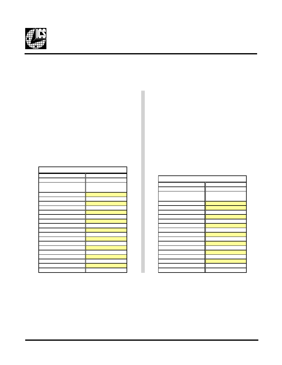
1.
The ICS clock generator is a slave/receiver, I
2
C component. It can read back the data stored in the latches for verification.
Read-Back will support Intel PIIX4 "Block-Read" protocol.
2.
The data transfer rate supported by this clock generator is 100K bits/sec or less (standard mode)
3.
The input is operating at 3.3V logic levels.
4.
The data byte format is 8 bit bytes.
5.
To simplify the clock generator I
2
C interface, the protocol is set to use only "Block-Writes" from the controller. The
bytes must be accessed in sequential order from lowest to highest byte with the ability to stop after any complete byte
has been transferred. The Command code and Byte count shown above must be sent, but the data is ignored for those
two bytes. The data is loaded until a Stop sequence is issued.
6.
At power-on, all registers are set to a default condition, as shown.
General I
2
C serial interface information
The information in this section assumes familiarity with I
2
C programming.
For more information, contact ICS for an I
2
C programming application note.
How to Write:
Controller (host) sends a start bit.
Controller (host) sends the write address D2
(H)
ICS clock will acknowledge
Controller (host) sends a dummy command code
ICS clock will acknowledge
Controller (host) sends a dummy byte count
ICS clock will acknowledge
Controller (host) starts sending first byte (Byte 0)
through byte 5
ICS clock will acknowledge each byte one at a time.
Controller (host) sends a Stop bit
How to Read:
Controller (host) will send start bit.
Controler (host) sends the read address D3
(H)
ICS clock will acknowledge
ICS clock will send the byte count
Controller (host) acknowledges
ICS clock sends first byte (Byte 0) through byte 5
Controller (host) will need to acknowledge each byte
Controller (host) will send a stop bit
Notes:
Controller (Host)
ICS (Slave/Receiver)
Start Bit
Address
D3
(H)
ACK
Byte Count
ACK
Byte 0
ACK
Byte 1
ACK
Byte 2
ACK
Byte 3
ACK
Byte 4
ACK
Byte 5
ACK
Stop Bit
How to Read:
Controller (Host)
ICS (Slave/Receiver)
Start Bit
Address
D2
(H)
ACK
Dummy Command Code
ACK
Dummy Byte Count
ACK
Byte 0
ACK
Byte 1
ACK
Byte 2
ACK
Byte 3
ACK
Byte 4
ACK
Byte 5
ACK
Stop Bit
How to Write:
4
ICS9179-06
Byte 2: OUTPUT Clock Register (Default = 1)
Notes: 1 = Enabled; 0 = Disabled, outputs held low
T
I
B
#
N
I
P
D
W
P
N
O
I
T
P
I
R
C
S
E
D
7
t
i
B
5
4
1
)
t
c
a
n
I
/
t
c
A
(
5
1
T
U
P
T
U
O
6
t
i
B
4
4
1
)
t
c
a
n
I
/
t
c
A
(
4
1
T
U
P
T
U
O
5
t
i
B
1
4
1
)
t
c
a
n
I
/
t
c
A
(
3
1
T
U
P
T
U
O
4
t
i
B
0
4
1
)
t
c
a
n
I
/
t
c
A
(
2
1
T
U
P
T
U
O
3
t
i
B
4
3
1
)
t
c
a
n
I
/
t
c
A
(
1
1
T
U
P
T
U
O
2
t
i
B
3
3
1
)
t
c
a
n
I
/
t
c
A
(
0
1
T
U
P
T
U
O
1
t
i
B
0
3
1
)
e
v
i
t
c
a
n
I
/
e
v
i
t
c
A
(
9
T
U
P
T
U
O
0
t
i
B
9
2
1
)
e
v
i
t
c
a
n
I
/
e
v
i
t
c
A
(
8
T
U
P
T
U
O
Byte 3: OUTPUT Clock Register
Notes: 1 = Enabled; 0 = Disabled, outputs held low
T
I
B
#
N
I
P
D
W
P
N
O
I
T
P
I
R
C
S
E
D
7
t
i
B
-
1
d
e
v
r
e
s
e
R
6
t
i
B
-
1
d
e
v
r
e
s
e
R
5
t
i
B
-
1
d
e
v
r
e
s
e
R
4
t
i
B
-
1
d
e
v
r
e
s
e
R
3
t
i
B
-
1
d
e
v
r
e
s
e
R
2
t
i
B
-
1
d
e
v
r
e
s
e
R
1
t
i
B
-
1
d
e
v
r
e
s
e
R
0
t
i
B
-
1
d
e
v
r
e
s
e
R
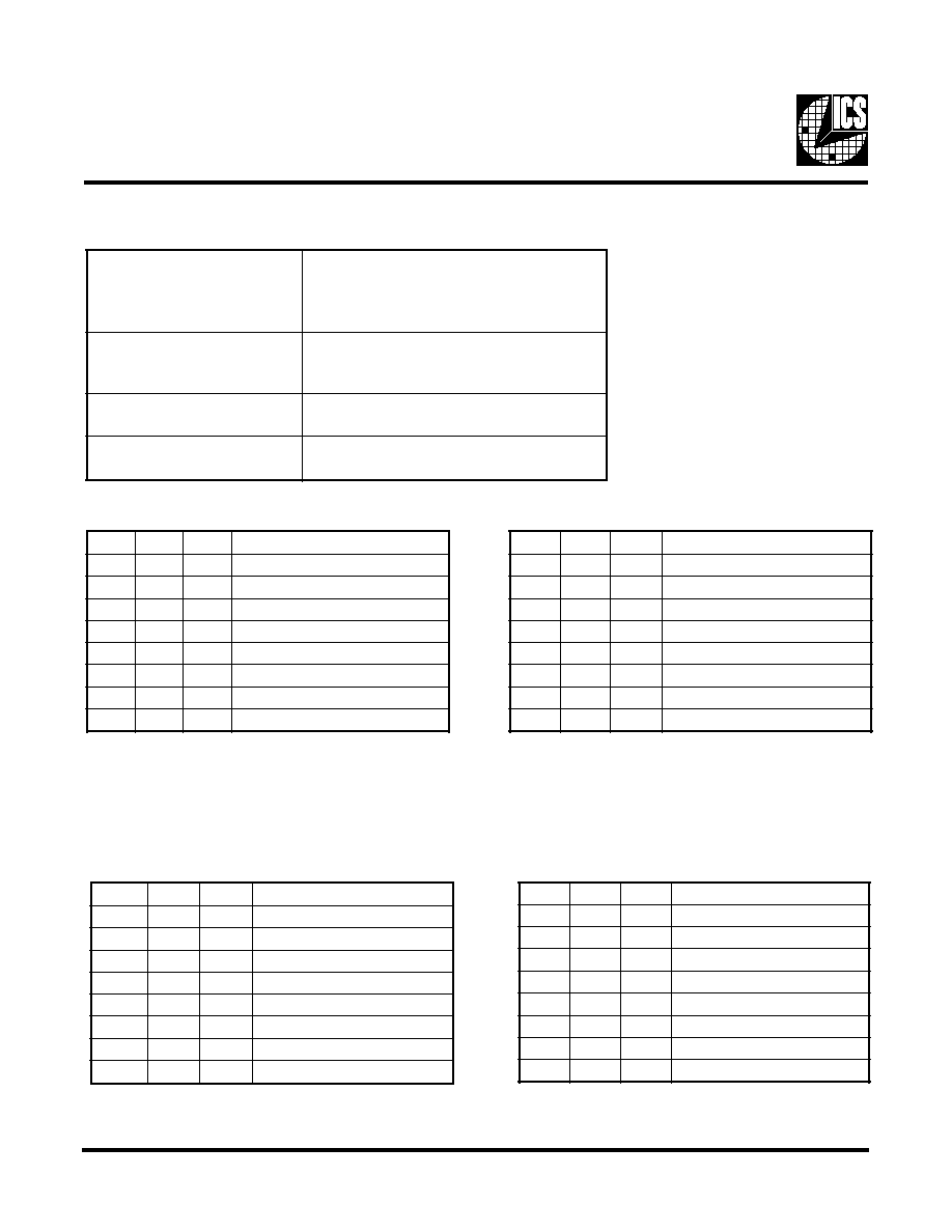
ICS9179-06 Power Management
The values below are estimates of target specifications.
n
o
i
t
i
d
n
o
C
n
o
i
t
p
m
u
s
n
o
c
y
l
p
p
u
s
V
3
.
3
x
a
M
s
d
a
o
l
p
a
c
e
t
e
r
c
s
i
d
x
a
M
V
5
6
4
.
3
=
D
D
V
D
N
G
r
o
D
D
V
=
s
t
u
p
n
i
c
i
t
a
t
s
l
l
A
e
d
o
M
k
c
o
l
C
o
N
)
D
N
G
r
o
1
D
D
V
-
N
I
_
F
U
B
(
I
2
e
v
i
t
c
A
y
r
t
i
u
c
r
i
C
C
A
m
0
3
z
H
M
6
6
e
v
i
t
c
A
)
z
H
M
6
6
.
6
6
=
N
I
_
F
U
B
(
A
m
0
5
1
z
H
M
0
0
1
e
v
i
t
c
A
)
z
H
M
0
0
.
0
0
1
=
N
I
_
F
U
B
(
A
m
0
8
1
Note: PWD = Power-Up Default
Byte 0: OUTPUT Clock Register (default = 0)
Notes: 2 = Default = 0; 1 = Delay element enabled,
0 = No delay path.
T
I
B
#
N
I
P
D
W
P
N
O
I
T
P
I
R
C
S
E
D
7
t
i
B
-
0
d
e
v
r
e
s
e
R
6
t
i
B
-
0
d
e
v
r
e
s
e
R
5
t
i
B
-
0
d
e
v
r
e
s
e
R
4
t
i
B
-
0
d
e
v
r
e
s
e
R
3
t
i
B
-
0
d
e
v
r
e
s
e
R
2
t
i
B
-
0
d
e
v
r
e
s
e
R
1
t
i
B
2
2
1
0
l
o
r
t
n
o
C
w
e
k
S
T
U
P
N
I
k
c
o
l
C
0
t
i
B
2
3
1
0
l
o
r
t
n
o
C
w
e
k
S
N
I
B
F
Serial Configuration Command Bitmaps
Notes: 1 = Enabled; 0 = Disabled, outputs held low
Byte 1: OUTPUT Clock Register
T
I
B
#
N
I
P
D
W
P
N
O
I
T
P
I
R
C
S
E
D
7
t
i
B
0
2
1
)
t
c
a
n
I
/
t
c
A
(
7
T
U
P
T
U
O
6
t
i
B
9
1
1
)
t
c
a
n
I
/
t
c
A
(
6
T
U
P
T
U
O
5
t
i
B
6
1
1
)
t
c
a
n
I
/
t
c
A
(
5
T
U
P
T
U
O
4
t
i
B
5
1
1
)
t
c
a
n
I
/
t
c
A
(
4
T
U
P
T
U
O
3
t
i
B
0
1
1
)
t
c
a
n
I
/
t
c
A
(
3
T
U
P
T
U
O
2
t
i
B
9
1
)
t
c
a
n
I
/
t
c
A
(
2
T
U
P
T
U
O
1
t
i
B
6
1
)
t
c
a
n
I
/
t
c
A
(
1
T
U
P
T
U
O
0
t
i
B
5
1
)
t
c
a
n
I
/
t
c
A
(
0
T
U
P
T
U
O
Note: PWD = Power-Up Default
5
ICS9179-06
Absolute Maximum Ratings
Supply Voltage . . . . . . . . . . . . . . . . . . . . . . . . . . 7.0 V
Logic Inputs . . . . . . . . . . . . . . . . . . . . . . . . . . . . GND 0.5 V to V
DD
+0.5 V
Ambient Operating Temperature . . . . . . . . . . . . 0°C to +70°C
Storage Temperature . . . . . . . . . . . . . . . . . . . . . 65°C to +150°C
Stresses above those listed under Absolute Maximum Ratings may cause permanent damage to the device. These ratings are
stress specifications only and functional operation of the device at these or any other conditions above those listed in the
operational sections of the specifications is not implied. Exposure to absolute maximum rating conditions for extended
periods may affect product reliability.
Electrical Characteristics - Input & Supply
T
A
= 0 - 70C; Supply Voltage V
DD
= 3.3 V +/-5% (unless otherwise stated)
PARAMETER
SYMBOL
CONDITIONS
MIN
TYP
MAX
UNITS
Input High Voltage
V
IH
2
V
DD
+0.3
V
Input Low Voltage
V
IL
V
SS
-0.3
0.8
V
Input High Current
I
IH
V
IN
= V
DD
5
uA
Input Low Current
I
IL1
V
IN
= 0 V; Inputs with no pull-up resistors
-5
uA
Input Low Current
I
IL2
V
IN
= 0 V; Inputs with pull-up resistors
-60
-33
uA
Operating
I
DD
C
L
= 0 pF; F
IN
@ 66M
115
150
mA
Supply Current
C
L
= 0 pF; F
IN
@ 100M
170
180
mA
Output Disabled
I
DD
C
L
= 0 pF; F
IN
@ 66M
30
mA
Supply Current
C
L
= 0 pF; F
IN
@ 100M
30
mA
Input frequency
F
i
V
DD
= 3.3 V; All Outputs Loaded
33
105
MHz
Input Capacitance
C
IN
Logic Inputs
5
pF
1
Guarenteed by design, not 100% tested in production.
Electrical Characteristics - Input & Supply
T
A
= 0 - 70C; Supply Voltage V
DD
= 3.3 V +/-5% (unless otherwise stated)
PARAMETER
SYMBOL
CONDITIONS
MIN
TYP
MAX
UNITS
Input High Voltage
V
IH
2
V
DD
+0.3
V
Input Low Voltage
V
IL
V
SS
-0.3
0.8
V
Input High Current
I
IH
V
IN
= V
DD
5
uA
I
IL
V
IN
= 0 V; Inputs with no pull-up resistors
-5
uA
I
IL
V
IN
= 0 V; Inputs with 100K pull-up resistors
-60
-33
uA
Operating
I
DD1
C
L
= 0 pF; F
IN
@ 66M
115
150
mA
Supply Current
I
DD2
C
L
= 0 pF; F
IN
@ 100M
170
180
mA
Input frequency
F
i
1
V
DD
= 3.3 V; All Outputs Loaded
10
150
MHz
Input Capacitance
C
IN
1
Logic Inputs
5
pF
1
Guarenteed by design, not 100% tested in production.
Input Low Current