87949AYI-147
www.icst.com/products/hiperclocks.html
REV. B NOVEMBER 21, 2002
1
Integrated
Circuit
Systems, Inc.
ICS87949I-147
L
OW
S
KEW
,
÷
1,
÷
2
C
LOCK
G
ENERATOR
G
ENERAL
D
ESCRIPTION
The ICS87949I-147 is a low skew, ÷1, ÷2 Clock
Generator and a member of the HiPerClockSTM
family of High Performance Clock Solutions from
ICS. The ICS87949I-147 has selectable single
ended clock or LVPECL clock inputs. The single
ended clock input accepts LVCMOS or LVTTL input levels.
The PCLK, nPCLK pair can accept LVPECL, CML, or SSTL
input levels. The low impedance LVCMOS outputs are de-
signed to drive 50
series or parallel terminated transmis-
sion lines. The effective fanout can be increased from 15 to
30 by utilizing the ability of the outputs to drive two series
terminated lines.
The divide select inputs, DIV_SELx, control the output fre-
quency of each bank. The outputs can be utilized in the ÷1,
÷2 or a combination of ÷1 and ÷2 modes. The master reset
input, MR/nOE, resets the internal frequency dividers and also
controls the active and high impedance states of all outputs.
The ICS87949I-147 is characterized at 3.3V and 2.5V. Guaran-
teed output and part-to-part skew characteristics make the
ICS87949I-147 ideal for those clock distribution applications
demanding well defined performance and repeatability.
F
EATURES
· 15 single ended LVCMOS outputs,
7
typical output impedance
· Selectable LVCMOS or LVPECL clock inputs
· CLK0 and CLK1 can accept the following input levels:
LVCMOS and LVTTL
· PCLK, nPCLK supports the following input types:
LVPECL, CML, SSTL
· Maximum input frequency: 250MHz
· Output skew: 250ps (maximum)
· Part-to-part skew: 1.0ns (maximum)
· 3.3V or 2.5V supply voltage
· -40°C to 85°C ambient operating temperature
· Pin compatible to the MPC949
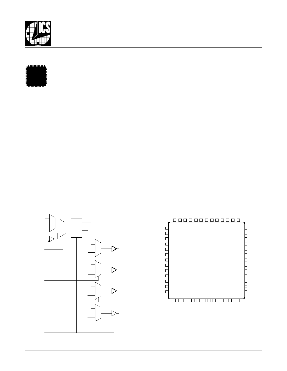
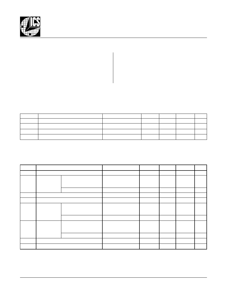
B
LOCK
D
IAGRAM
P
IN
A
SSIGNMENT
52-Lead LQFP
10mm x 10mm x 1.4mm package body
Y Package
Top View
HiPerClockSTM
,&6
nc
V
DDD
QD4
GND
QD3
V
DDD
QD2
GND
QD1
V
DDD
QD0
GND
nc
MR/nOE
CLK_SEL
V
DD
CLK0
CLK1
PCLK
nPCLK
PCLK_SEL
DIV_SELA
DIV_SELB
DIV_SELC
DIV_SELD
GND
1
2
3
4
5
6
7
8
9
10
11
12
13
14 15 16 17 18 19 20 21 22 23 24 25 26
39
38
37
36
35
34
33
32
31
30
29
28
27
52 51 50 49 48 47 46 45 44 43 42 41 40
nc
GND
QC0
V
DDC
QC1
GND
QC2
V
DDC
QC3
GND
GND
QD5
nc
nc
V
DDB
QB2
GND
QB1
V
DDB
QB0
GND
GND
QA1
V
DDA
QA0
GND
ICS87949I-147
DIV_SELA
DIV_SELB
DIV_SELC
DIV_SELD
MR/nOE
QA0:QA1
QB0:QB2
QC0:QC3
QD0:QD5
CLK_SEL
CLK0
CLK1
PCLK
nPCLK
PCLK_SEL
0
1
÷
1
÷
2
0
1
0
1
0
1
0
1
R
0
1
87949AYI-147
www.icst.com/products/hiperclocks.html
REV. B NOVEMBER 21, 2002
4
Integrated
Circuit
Systems, Inc.
ICS87949I-147
L
OW
S
KEW
,
÷
1,
÷
2
C
LOCK
G
ENERATOR
T
ABLE
4A. P
OWER
S
UPPLY
DC C
HARACTERISTICS
,
V
DD
= V
DD
X
= 3.3V ± 0.3V, T
A
= -40°C
TO
85°C
T
ABLE
4B. DC C
HARACTERISTICS
,
V
DD
= V
DD
X
= 3.3V ± 0.3V, T
A
= -40°C
TO
85°C
l
o
b
m
y
S
r
e
t
e
m
a
r
a
P
s
n
o
i
t
i
d
n
o
C
t
s
e
T
m
u
m
i
n
i
M
l
a
c
i
p
y
T
m
u
m
i
x
a
M
s
t
i
n
U
V
D
D
e
g
a
t
l
o
V
y
l
p
p
u
S
e
r
o
C
5
3
1
.
3
3
.
3
5
6
4
.
3
V
V
x
D
D
1
E
T
O
N
;
e
g
a
t
l
o
V
y
l
p
p
u
S
t
u
p
t
u
O
5
3
1
.
3
3
.
3
5
6
4
.
3
V
I
D
D
t
n
e
r
r
u
C
y
l
p
p
u
S
r
e
w
o
P
e
r
o
C
0
6
A
m
I
x
D
D
2
E
T
O
N
;
t
n
e
r
r
u
C
y
l
p
p
u
S
r
e
w
o
P
t
u
p
t
u
O
0
2
A
m
V
:
1
E
T
O
N
x
D
D
V
s
e
t
o
n
e
d
A
D
D
, V
B
D
D
, V
C
D
D
, V
D
D
D
.
I
:
2
E
T
O
N
x
D
D
I
f
o
m
u
s
e
h
t
s
e
t
o
n
e
d
A
D
D
, I
B
D
D
, I
C
D
D
, I
D
D
D
.
l
o
b
m
y
S
r
e
t
e
m
a
r
a
P
s
n
o
i
t
i
d
n
o
C
t
s
e
T
m
u
m
i
n
i
M
l
a
c
i
p
y
T
m
u
m
i
x
a
M
s
t
i
n
U
V
H
I
e
g
a
t
l
o
V
h
g
i
H
t
u
p
n
I
2
V
D
D
3
.
0
+
V
V
L
I
t
u
p
n
I
e
g
a
t
l
o
V
w
o
L
,
D
L
E
S
_
V
I
D
:
A
L
E
S
_
V
I
D
,
L
E
S
_
K
L
C
,
L
E
S
_
K
L
C
P
E
O
n
/
R
M
3
.
0
-
8
.
0
V
1
K
L
C
,
0
K
L
C
3
.
0
-
3
.
1
V
V
P
P
e
g
a
t
l
o
V
t
u
p
n
I
k
a
e
P
-
o
t
-
k
a
e
P
3
.
0
1
V
V
R
M
C
2
,
1
E
T
O
N
;
e
g
a
t
l
o
V
t
u
p
n
I
e
d
o
M
n
o
m
m
o
C
5
.
1
+
D
N
G
V
D
D
V
I
H
I
t
u
p
n
I
t
n
e
r
r
u
C
h
g
i
H
,
D
L
E
S
_
V
I
D
:
A
L
E
S
_
V
I
D
,
L
E
S
_
K
L
C
P
,
L
E
S
_
K
L
C
E
O
n
/
R
M
V
D
D
V
=
N
I
V
5
6
4
.
3
=
0
5
1
A
µ
1
K
L
C
,
0
K
L
C
V
D
D
V
=
N
I
V
5
6
4
.
3
=
5
A
µ
I
L
I
t
u
p
n
I
t
n
e
r
r
u
C
w
o
L
,
D
L
E
S
_
V
I
D
:
A
L
E
S
_
V
I
D
,
L
E
S
_
K
L
C
P
,
L
E
S
_
K
L
C
E
O
n
/
R
M
V
D
D
V
,
V
5
6
4
.
3
=
N
I
V
0
=
5
-
A
µ
1
K
L
C
,
0
K
L
C
V
D
D
V
,
V
5
6
4
.
3
=
N
I
V
0
=
0
5
1
-
A
µ
V
H
O
e
g
a
t
l
o
V
h
g
i
H
t
u
p
t
u
O
I
H
O
A
m
0
2
-
=
5
.
2
V
V
L
O
e
g
a
t
l
o
V
w
o
L
t
u
p
t
u
O
I
L
O
A
m
0
2
=
4
.
0
V
V
s
a
d
e
n
i
f
e
d
s
i
e
g
a
t
l
o
v
e
d
o
m
n
o
m
m
o
C
:
1
E
T
O
N
H
I
.
s
n
o
i
t
a
c
il
p
p
a
d
e
d
n
e
e
l
g
n
i
s
r
o
F
:
2
E
T
O
N
,
V
s
i
K
L
C
P
n
d
n
a
K
L
C
P
r
o
f
e
g
a
t
l
o
v
t
u
p
n
i
m
u
m
i
x
a
m
e
h
t
D
D
.
V
3
.
0
+
A
BSOLUTE
M
AXIMUM
R
ATINGS
Supply Voltage, V
DD
4.6V
Inputs, V
I
-0.5V to V
DD
+ 0.5 V
Outputs, V
O
-0.5V to V
DD
+ 0.5V
Package Thermal Impedance,
JA
42.3°C/W (0 lfpm)
Storage Temperature, T
STG
-65°C to 150°C
NOTE: Stresses beyond those listed under Absolute
Maximum Ratings may cause permanent damage to the
device. These ratings are stress specifications only. Functional
operation of product at these conditions or any conditions be-
yond those listed in the
DC Characteristics or AC Character-
istics is not implied. Exposure to absolute maximum rating
conditions for extended periods may affect product reliability.