 | –≠–Ľ–Ķ–ļ—ā—Ä–ĺ–Ĺ–Ĺ—č–Ļ –ļ–ĺ–ľ–Ņ–ĺ–Ĺ–Ķ–Ĺ—ā: 750FX | –°–ļ–į—á–į—ā—Ć:  PDF PDF  ZIP ZIP |

IBM PowerPC
ģ
750FX RISC Microprocessor
Datasheet
(Support for 750FX Design Revision Level DD 2.X)
Version: 2.0
Preliminary
June 9, 2003
ģ

ģ
Copyright and Disclaimer
© Copyright International Business Machines Corporation 2003
All Rights Reserved
Printed in the United States of America June 2003
The following are trademarks of International Business Machines Corporation in the United States, or other countries,
or both.
IBM
IBM Logo
PowerPC
PowerPC Logo
PowerPC 750
PowerPC Architecture
RISCWatch
Other company, product and service names may be trademarks or service marks of others.
All information contained in this document is subject to change without notice. The products described in this document
are NOT intended for use in applications such as implantation, life support, or other hazardous uses where malfunction
could result in death, bodily injury, or catastrophic property damage. The information contained in this document does not
affect or change IBM product specifications or warranties. Nothing in this document shall operate as an express or implied
license or indemnity under the intellectual property rights of IBM or third parties. All information contained in this docu-
ment was obtained in specific environments, and is presented as an illustration. The results obtained in other operating
environments may vary.
While the information contained herein is believed to be accurate, such information is preliminary, and should not be
relied upon for accuracy or completeness, and no representations or warranties of accuracy or completeness are made.
THE INFORMATION CONTAINED IN THIS DOCUMENT IS PROVIDED ON AN "AS IS" BASIS. In no event will IBM be
liable for damages arising directly or indirectly from any use of the information contained in this document.
IBM Microelectronics Division
1580 Route 52, Bldg. 504
Hopewell Junction, NY 12533-6351
The IBM home page can be found at
http://www.ibm.com
The IBM Microelectronics Division home page
can be found at
http://www-3.ibm.com/chips/
Title_750FX_DS_DD2.X.fm.2.0
June 9, 2003
Preliminary
Note: This document contains information on products in the sampling and/or initial production phases of
development. This information is subject to change without notice. Verify with your IBM field applications
engineer that you have the latest version of this document before finalizing a design.

Datasheet
DD 2.X
Preliminary
PowerPC 750FX RISC Microprocessor
750FX_DS_DD2.X_V2.02.fm.2.0
June 9, 2003
Page 1 of 63
1. General Information .................................................................................................... 3
1.1 Features ............................................................................................................................................ 3
1.2 Design Level Considerations and Features ...................................................................................... 5
1.3 Processor Version Register .............................................................................................................. 5
1.4 Part Number Information ................................................................................................................... 6
2. Overview ...................................................................................................................... 7
2.1 Block Diagram ................................................................................................................................... 7
2.2 General Parameters .......................................................................................................................... 8
3. Electrical and Thermal Characteristics ..................................................................... 9
3.1 DC Electrical Characteristics ............................................................................................................. 9
3.2 Clock AC Specifications .................................................................................................................. 13
3.3 Spread Spectrum Clock Generator (SSCG) ................................................................................... 14
3.5 60x Bus Output AC Specifications .................................................................................................. 17
3.6 Alternate I/O Timing For 3.3V Bus .................................................................................................. 19
3.6.1 IEEE 1149.1 AC Timing Specifications ................................................................................. 20
4. Dimensions and Signal Assignments ..................................................................... 22
4.1 Module Substrate Decoupling Voltage Assignments ...................................................................... 22
4.2 Package .......................................................................................................................................... 22
4.3 Microprocessor Ball Placement ....................................................................................................... 24
5. System Design Information ..................................................................................... 31
5.1 PLL Considerations ......................................................................................................................... 31
5.1.1 Restrictions and Considerations for PLL Configuration ......................................................... 32
5.1.1.1 Configuration Restriction on Frequency Transitions ...................................................... 32
5.1.2 PLL_RNG[0:1] Definitions for Dual PLL Operation ................................................................ 32
5.1.3 PLL Configuration .................................................................................................................. 33
5.2 PLL Power Supply Filtering ............................................................................................................. 35
5.3 Decoupling Recommendations ....................................................................................................... 39
5.4 Output Buffer DC Impedance .......................................................................................................... 42
5.4.1 Input-Output Usage ............................................................................................................... 43
5.5 Level Protection .............................................................................................................................. 48
5.6 64 or 32-Bit Data Bus Mode ............................................................................................................ 49
5.7 IIO Voltage Mode Selection ............................................................................................................ 49
5.8 Thermal Management ..................................................................................................................... 49
5.8.1 Heat Sink Selection Example ................................................................................................ 49
5.8.2 Internal Package Conduction ................................................................................................ 52
5.8.3 Minimum Heat Sink Requirements ........................................................................................ 53
5.8.4 Heat Sink Mounting ............................................................................................................... 54
5.8.5 Thermal Assist Unit ............................................................................................................... 54
5.8.6 Adhesives and Thermal Interface Materials .......................................................................... 55
5.8.7 Thermal Interface and Adhesive Vendors ............................................................................. 56
5.8.8 Heat Sink Vendors ................................................................................................................. 57
Revision Log ................................................................................................................ 59

Datasheet
DD 2.X
PowerPC 750FX RISC Microprocessor
Preliminary
Page 2 of 63
750FX_DS_DD2.X_V2.02.fm.2.0
June 9, 2003

DD 2.X
Preliminary
PowerPC 750FX RISC Microprocessor
Body_750FX_DS_DD2.X.fm.2.0
June 9, 2003
1. General Information
Page 3 of 63
1. General Information
The IBM PowerPC
ģ
750FX RISC Microprocessor is a 32-bit implementation of the IBM PowerPC family of
reduced instruction set computer (RISC) microprocessors. This document contains pertinent physical and
electrical characteristics of the IBM PowerPC 750FX RISC Microprocessor Revision DD 2.X Single Chip
Modules (SCM). The IBM PowerPC 750FX RISC Microprocessor is also referred to as the 750FX throughout
this document.
1.1 Features
This section summarizes the features of the 750FX
implementation of the PowerPC ArchitectureTM.
Major features of the 750FX include the following:
∑ Branch processing unit
≠ Four instructions fetched per clock
≠ One branch processed per cycle (plus
resolving two speculations)
≠ Up to one speculative stream in execution,
one additional speculative stream in fetch
≠ 512-entry branch history table (BHT) for
dynamic prediction
≠ 64-entry, 4-way set associative branch
target instruction cache (BTIC) for
eliminating branch delay slots
∑ Decode
≠ Register file access
≠ Forwarding control
≠ Partial instruction decode
∑ Load/store unit
≠ One cycle load or store cache access (byte,
half-word, word, double-word)
≠ Effective address generation
≠ Hits under miss (one outstanding miss)
≠ Single-cycle misaligned access within
double-word boundary
≠ Alignment, zero padding, sign extend for
integer register file
≠ Floating-point internal format conversion
(alignment, normalization)
≠ Sequencing for load/store multiples and
string operations
≠ Store gathering
≠ Cache and TLB instructions
≠ Big and little-endian byte addressing
supported
≠ Misaligned little-endian support in hardware
∑ Dispatch unit
≠ Full hardware detection of dependencies
(resolved in the execution units)
≠ Dispatch two instructions to six independent
units (system, branch, load/store, fixed-point
unit 1, fixed-point unit 2, or floating-point)
≠ 4-stage pipeline: fetch, dispatch, execute,
and complete
≠ Serialization control (predispatch,
postdispatch, execution, serialization)
∑ Fixed-point units
≠ Fixed-point unit 1 (FXU1): multiply, divide,
shift, rotate, arithmetic, logical
≠ Fixed-point unit 2 (FXU2): shift, rotate,
arithmetic, logical
≠ Single-cycle arithmetic, shift, rotate, logical
≠ Multiply and divide support (multi-cycle)
≠ Early out multiply
≠ Thirty-two 32-bit general purpose registers
∑ Floating-point unit
≠ Support for IEEE-754 standard single and
double-precision floating-point arithmetic
≠ Optimized for single-precision multiply/add
≠ Thirty-two, 64-bit floating point registers
≠ Enhanced reciprocal estimates
≠ 3-cycle latency, 1-cycle throughput,
single-precision multiply-add
≠ 3-cycle latency, 1-cycle throughput,
double-precision add
≠ 4-cycle latency, 2-cycle throughput,
double-precision multiply-add
≠ Hardware support for divide
≠ Hardware support for denormalized
numbers
≠ Time deterministic non-IEEE mode
∑ System unit
≠ Executes CR logical instructions and mis-
cellaneous system instructions
≠ Special register transfer instructions
.

Body_750FX_DS_DD2.X.fm.2.0
June 9, 2003
1. General Information
Page 4 of 63
PowerPC 750FX RISC Microprocessor
Preliminary
∑ L1 Cache structure
≠ 32K, 32-byte line, 8-way set associative
instruction cache
≠ 32K, 32-byte line, 8-way set associative
data cache
≠ Single-cycle cache access
≠ Pseudo-LRU replacement
≠ Copy-back or write-through data cache (on
a page per page basis)
≠ Parity on L1 tags and arrays
≠ 3-state (MEI) memory coherency
≠ Hardware support for data coherency
≠ Non-blocking instruction cache (one out-
standing miss)
≠ Non-blocking data cache (two outstanding
misses)
≠ No snooping of instruction cache
∑ Memory management unit
≠ 64 entry, 2-way set associative instruction
TLB (total 128)
≠ 64 entry, 2-way set associative data TLB
(total 128)
≠ Hardware reload for TLBs
≠ 8 instruction BATs and 8 data BATs
≠ Virtual memory support for up to 4 exabytes
(2
52
) virtual memory
≠ Real memory support for up to 4 gigabytes
(2
32
) of physical memory
≠ Support for big/little-endian addressing
∑ Dual PLLs
≠ Allows seamless frequency switching
∑ Level 2 (L2) cache
≠ Internal L2 cache controller and 4K-entry
tags: 512KB data SRAMs
≠ Two-way set-associative, supports locking
by way
≠ Copy-back or write-through data cache on a
page basis, or for all L2
≠ 64-byte sectored line size
≠ L2 frequency at core speed
≠ ECC protection on SRAM array
≠ Parity on L2 tags
≠ Supports up to 2 outstanding misses
(1 data and 1 instruction or 2 data)
∑ Power
≠ Low power consumption with low voltage
application at lower frequency
≠ Dynamic power management
≠ 3 static power save modes
(doze, nap, and sleep)
≠ Thermal Assist Unit (TAU)
∑ Bus interface
≠ 32-bit address bus
≠ 64-bit data bus (also supports 32-bit mode)
≠ Enhanced 60x bus: pipelines consecutive
reads to a depth of 2
≠ Core-to-bus frequency multipliers of 3.5x,
4x, 4.5x, 5x, 5.5x, 6x, 6.5x, 7x, 7.5x, 8x,
8.5x, 9x, 9.5x, 10x, 11x, 12x, 13x, 14x, 15x,
16x, 17x, 18x, 19x, and 20x supported
≠ Supports 1.8V, 2.5V, or 3.3V I/O modes
∑ Reliability and serviceability
- Parity checking on 60x interface
- ECC checking on L2 cache
- Parity on the L1 arrays
- Parity on the L1 and L2 tags
∑ Testability
≠ LSSD scan design
≠ Powerful diagnostic and test interface
through Common On-Chip Processor
(COP) and IEEE 1149.1 (JTAG) interface

DD 2.X
Preliminary
PowerPC 750FX RISC Microprocessor
Body_750FX_DS_DD2.X.fm.2.0
June 9, 2003
1. General Information
Page 5 of 63
1.2 Design Level Considerations and Features
The 750FX supports several unique features including those listed below. The IBM application note Differ-
ences between the PowerPC 750FX, 750, 750CX, and 750CXe Microprocessors provides a more detailed
explanation of these features.
∑ Incorporates an on-chip, 512K, two-way, set-associative L2 cache
∑ Provides a 64 or 32-bit Data Bus mode (per setup of TLBISYNC pin)
∑ Supports 1.8V, 2.5V, or 3.3V I/O modes
Implementation Note: DD2.0 supports a limited use of the 3.3V I/O mode. For additional
information, see the 750FX Errata List of Revision DD2.X.
∑ Includes all 60x bus pins on earlier PowerPC 750 designs and additional signals
∑ Enhanced 60x bus -- for pipelined consecutive read transactions and higher frequency operation
∑ Dual PLLs for additional power savings capabilities
∑ Four additional IBAT/DBAT registers
∑ New CBGA package with additional pins and depopulated footprint
1.3 Processor Version Register
The PowerPC 750FX RISC Microprocessor has the following Processor Version Register (PVR) values for
the respective design revision levels.
The 750FX PVR is 7000, which is not used in any previous PowerPC processor design.
Table 1-1. 750FX Processor Version Register (PVR)
750FX Design Revision Level
750FX PVR
DD2.0
0x700a02b0
DD2.1
0x700a02b1
DD2.2
0x700a02b2
DD2.3
0x700a02b3
Note:
1. Nibbles shown as `b' are to be ignored, and are for factory use only. Nibbles shown as `a' may be 0 or 1
2. If L2_TSTCLK is pulled low, the PVR may read 0x000802b_. L2TSTCLK should be pulled up for normal operation.

DD 2.X
PowerPC 750FX RISC Microprocessor
Preliminary
1. General Information
Page 6 of 63
Body_750FX_DS_DD2.X.fm.2.0
June 9, 2003
1.4 Part Number Information
Figure 1-1. Part Number Legend
IBM25PPC750FX-GB
PowerPC 750 Family Member
Process Technology
Test Conditions
Shipping Container
Reliability Grade
Performance Sort
Package Type
Design Revision Level
Note: See the Datasheet Supplement for additional application conditions.
Process Technology
"--" = 0.13
Ķ
m CSOI
Design Revision Level
D = DD2.0
E = DD2.1
F = DD2.2
G = DD2.3
Package Type
B = Ceramic Ball Grid Array
Performance Sort
01 = Nominal at 600 MHz
05 = Nominal at 700 MHz
10 = Nominal at 733 MHz
25 = Nominal at 800 MHz
Test Conditions
1 = (see Datasheet Supplement and PCN-IBM-050803
2 = Special Test Conditions
3 = 1.4 - 1.5V @ 105
į
C
Reliability Grade
3 = Grade 3, <100 FIT AFR
2 = Grade 2, < 25 FIT AFR
Shipping Container
T = Tray
yy x3T

DD 2.X
Preliminary
PowerPC 750FX RISC Microprocessor
Body_750FX_DS_DD2.X.fm.2.0
June 9, 2003
2. Overview
Page 7 of 63
2. Overview
The PowerPC 750FX RISC Microprocessor, also called the 750FX, is targeted for high performance, low
power systems using a 60x bus. The 750FX also includes an internal 512KB L2 cache with on-board
Error Correction Circuitry (ECC).
2.1 Block Diagram
Figure 2-1 shows a block diagram of the PowerPC 750FX RISC Microprocessor.
Figure 2-1. PowerPC 750FX RISC Microprocessor Block Diagram
GPRs
LSU
FPU
Instruction Fetch
System
Completion
Rename
Buffers
Unit
32KB I-Cache
BHT /
Enhanced
L2 Cache
FXU2
Dispatch
Branch Unit
BTIC
Control Unit
FPRs
Rename
Buffers
512KB
32KB D-Cache
L2 Tags
FXU1
w/ECC
60x
BIU
with parity
with Parity
with parity

DD 2.X
PowerPC 750FX RISC Microprocessor
Preliminary
2. Overview
Page 8 of 63
Body_750FX_DS_DD2.X.fm.2.0
June 9, 2003
2.2 General Parameters
Table 2-1 provides a summary of the general parameters of the 750FX.
Table 2-1. 750FX General Parameters
Item
Description
Notes
Technology
0.13
Ķ
m CSOI technology, six-layer metallization plus one level of local interconnect
Die Size
34.3 sq. mm
Transistor count
38 million - including L2 cache
Logic design
Fully-static
Package
292-pin ceramic ball grid array (CBGA)
21x21mm (1.0 mm pitch)
0.8 mm ball size
Core power supply
1.45V +/- 50 mV
1
I/O power supply
3.3V +/- 165mV (BVSEL = 1, L1_TSTCLK = 0) or
2.5V +/- 125mV (BVSEL = 1, L1_TSTCLK = 1) or
1.8V +/- 100mV (BVSEL = 0, L1_TSTCLK = 1)
2
Note:
1. In some cases, when using 1.8v or 2.5v IO mode, it is possible to reduce power dissipation by lowering the core power supply volt-
age. See the Datasheet Supplement for details.
2. BVSEL =0, L1_TSTCLK = 0 is an INVALID setting. DD2.0 supports only a limited use of 3.3v IO mode. See the 750FX Errata List
for revision DD2.x for more information.

DD 2.X
Preliminary
PowerPC 750FX RISC Microprocessor
Body_750FX_DS_DD2.X.fm.2.0
June 9, 2003
3. Electrical and Thermal Characteristics
Page 9 of 63
3. Electrical and Thermal Characteristics
This section provides AC and DC electrical specifications and thermal characteristics for the 750FX.
3.1 DC Electrical Characteristics
The tables in this section describe the DC electrical characteristics for the 750FX.
Table 3-1. Absolute Maximum Ratings
1
Characteristic
Symbol
1.8V
2.5V
3.3V
Unit
Notes
Core supply voltage
V
DD
-0.3 to 1.6
-0.3 to 1.6
-0.3 to 1.6
V
3, 4
PLL supply voltage
A1V
DD
, A2V
DD
-0.3 to 1.6
-0.3 to 1.6
-0.3 to 1.6
V
3, 4, 5
60x bus supply voltage
OV
DD
-0.3 to 2.0
-0.3 to 2.75
-0.3 to 3.7
V
3, 4
Input voltage
V
IN
-0.3 to 2.0
-0.3 to 2.75
-0.3 to 3.7
V
2
Storage temperature range
T
STG
-55 to 150
-55 to 150
-55 to 150
į
C
Notes:
1. Functional and tested operating conditions are given in Table 3-2, "Recommended Operating Conditions" on page 10. Absolute
maximum ratings are stress ratings only, and functional operation at the maximums is not guaranteed. Stresses beyond those
listed above may affect device reliability or cause permanent damage to the device.
2. Caution: Transient V
IN
overshoots of up to OV
DD
+ 0.8V, with a maximum of 4.0V for 3.3V operation, and undershoots down to
GND - 0.8V, are allowed for up to 5ns.
3. Caution: OV
DD
must not exceed V
DD
/AV
DD
by more than 2.1V continuously. OV
DD
may exceed V
DD
/AV
DD
by up to 2.3V for up
to 20ms during power-on or power-off. OV
DD
must not exceed V
DD
/AV
DD
by more than 2.3V for any amount of time.
4. Caution: V
DD
/AV
DD
must not exceed OV
DD
by more than 1.0V continuously. V
DD
/AV
DD
may exceed OV
DD
by up to 1.6v for up
to 20ms during power-on or power-off. V
DD
/AV
DD
must not exceed OV
DD
by more than 1.6V for any amount of time.
5. Caution: AV
DD
must not exceed V
DD
by more than 0.5V at any time.

DD 2.X
PowerPC 750FX RISC Microprocessor
Preliminary
3. Electrical and Thermal Characteristics
Page 10 of 63
Body_750FX_DS_DD2.X.fm.2.0
June 9, 2003
Note: All electrical specifications (AC, DC, timing) are guaranteed only while the device is operated within
the recommended operating conditions (see Table 3-2). Operation at other application conditions may also
be possible; see the PowerPC 750FX RISC Microprocessor Datasheet Supplement for details.
Table 3-2. Recommended Operating Conditions
Characteristic
Symbol
Value
Unit
Notes
Core supply voltage (full-on mode)
V
DD
1.4 to 1.5
V
1, 2
Low Voltage (Low Frequency Operation, 1.8V and 2.5V
bus modes only)
V
DD
1.2 Minimum
V
1
PLL supply voltage
AV
DD
1.4 to 1.5
V
2
60x bus supply voltage (1.8V)
OV
DD
1.7 to 1.9
V
2
60x bus supply voltage (2.5V)
OV
DD
2.375 to 2.625
V
2
60x bus supply voltage (3.3V)
OV
DD
3.135 to 3.465
V
Input voltage
V
IN
GND to OV
DD
V
2
Die-junction temperature DD2.0 and 2.1
T
J
0 to 105
į
C
Die-junction temperature DD2.2 and 2.3
T
J
-40 to 105
Notes:
1. In some cases, when using 1.8v or 2.5v IO mode, it is possible to reduce power dissipation by lowering the core power supply volt-
age. See the Datasheet Supplement for details.
2. These are tested operating conditions.
Table 3-3. Package Thermal Characteristics
1
Characteristic
Symbol
2
Value
Unit
CBGA package thermal resistance, junction-to-case thermal resistance (typical)
JC
0.06
į
C/W
CBGA package thermal resistance, junction-to-lead thermal resistance (typical)
JB
7.6
į
C/W
Notes:
1. A heat sink is required (see Section 5.8 Thermal Management on page 49).
2.
JC
is the internal resistance from the junction to the back of the die. For more information about thermal management, see
Section 5.8 Thermal Management on page 49.

DD 2.X
Preliminary
PowerPC 750FX RISC Microprocessor
Body_750FX_DS_DD2.X.fm.2.0
June 9, 2003
3. Electrical and Thermal Characteristics
Page 11 of 63
Table 3-4. DC Electrical Specifications
See Table 3-2 on page 10 for recommended operating conditions.
Characteristic
Symbol
Voltage
Unit
Notes
Min
Max
Input high voltage (all inputs except SYSCLK)
V
IH (1.8V)
1.20
V
V
IH(2.5V)
1.70
V
V
IH(3.3V)
2.1
V
Input low voltage (all inputs except SYSCLK)
V
IL(1.8V
)
0.60
V
V
IL(2.5V)
0.70
V
V
IL(3.3V)
0.80
V
SYSCLK input high voltage
CV
IH(1.8V)
1.20
V
CV
IH(2.5V)
1.90
V
CV
IH(3.3V)
2.1
V
SYSCLK input low voltage
CV
IL(1.8V)
0.40
V
Input leakage current, V
IN
= applies to all OV
DD
levels
I
IN
20
Ķ
A
2
Hi-Z (off state) leakage current, V
IN
= applies to all OV
DD
levels
I
TSI
20
Ķ
A
2
Output high voltage, I
OH
= ≠4mA
V
OH(1.8V)
1.30
V
V
OH(2.5V)
2.00
V
V
OH(3.3V)
2.40
V
Output low voltage, I
OL
= 4mA
V
OL(1.8V, 2.5V, 3.3V)
0.4
V
Capacitance, V
IN
=0 V, f = 1MHz
C
IN
5
pF
1
Notes:
1.
Capacitance values are guaranteed by design and characterization, and are not tested
.
2.
Additional input current may be attributed to the Level Protection Keeper Lock circuitry. For details, see
Section 5.5 Level Protection
on page 48.

DD 2.X
PowerPC 750FX RISC Microprocessor
Preliminary
3. Electrical and Thermal Characteristics
Page 12 of 63
Body_750FX_DS_DD2.X.fm.2.0
June 9, 2003
Previous revisions of this datasheet showed incorrectly low power dissipation values. The power dissipation
of the 750FX has not increased, the datasheet has only been corrected to show the actual values.
Table 3-5. Power Consumption
See Table 3-2 on page 10 for recommended operating conditions.
Mode
V
DD
T
j
Representative Processor Frequency (see note 6)
Unit
Notes
400 MHz
600 MHz
700 MHz
733 MHz
800 MHz
Full-On Mode
Maximum
1.45V
105įC
7.1
7.9
8.2
8.3
8.6
1, 2
1.5V
105įC
7.9
8.7
9.3
9.4
9.7
1, 2
Typical
1.45V
85įC
3.9
4.6
5.0
5.1
5.4
1, 3
Nap Mode
Typical
1.45V
50įC
1.4
1.5
1.6
1.6
1.6
W
1
Sleep Mode
Typical
1.45V
50įC
1.4
1.4
1.4
1.4
1.4
W
1
Notes:
1. These values apply for all valid 60x buses. The values do not include I/O Supply Power (OV
DD
) or PLL/DLL supply power (AV
DD
). OV
DD
power is sys-
tem dependent, but is typically <2% of V
DD
power. AV
DD
current is less than 25mA each for AV
DD1
and AV
DD2
.
2. Maximum power is specified for fastest (worst process) parts running RC5 at the indicated core voltage, junction temperature, and core frequency.
3. Typical power is specified for median process 800 MHz parts0 running RC5 at the indicated core voltage, junction temperature, and core frequency.
The value is then adjusted for 13% less switching (AC component for P
D
) to account for the differences between RC5 and more typical application
code.

DD 2.X
Preliminary
PowerPC 750FX RISC Microprocessor
Body_750FX_DS_DD2.X.fm.2.0
June 9, 2003
3. Electrical and Thermal Characteristics
Page 13 of 63
3.2 Clock AC Specifications
Table 3-6 provides the clock AC timing specifications as defined in Figure 3-1.
Table 3-6. Clock AC Timing Specifications (See Table 3-2 on page 10 for recommended operating
conditions
1,6
)
Num
(Timing Reference)
Characteristic
Value
Unit
Notes
Min.
Max.
Processor frequency
400
800
MHz
7
SYSCLK frequency
20
200
MHz
1, 6
1
SYSCLK cycle time
5.0
50
ns
2, 3
SYSCLK rise and fall slew rate
1.0
--
V/ns
3
4
SYSCLK duty cycle measured at 0.8V
25
75
%
3
VM
SYSCLK
Measurement Reference Voltage for SYSCLK (all I/O voltages)
0.65
V
SYSCLK cycle-to-cycle jitter
≠
Ī
150
ps
4, 3
Internal PLL relock time
≠
100
Ķ
s
5
Notes:
1. Caution: The SYSCLK frequency and the PLL_CFG[0:4] settings must be chosen such that the resulting SYSCLK (bus)
frequency, CPU (core) frequency, and PLL frequency do not exceed their respective maximum or minimum operating frequencies.
Refer to the PLL_CFG[0:4] signal description in Table 5-2, "750FX Microprocessor PLL Configuration" on page 33 for valid
PLL_CFG[0:4] settings.
2. The SYSCLK slew rate applies between 0.4V and 1.0V.
3. Timing is guaranteed by design and characterization, and is not tested.
4. See Section 3.3 Spread Spectrum Clock Generator (SSCG) on page 14 for long term jitter.
5. Relock timing is guaranteed by design and characterization, and is not tested. PLL-relock time is the maximum amount of time
required for PLL lock after a stable V
DD
and SYSCLK are reached during the power-on reset sequence. This specification also
applies when the PLL has been disabled and subsequently re-enabled during sleep mode. Also note that HRESET must be held
asserted for a minimum of 255 bus clocks after the PLL-relock time during the power-on reset sequence.
6. This is a statement of the capability of the 750FX I/O circuitry. Not all systems can run at the maximum SYSCLK frequency. Con-
tact IBM PowerPC Application Engineering for more information on high-speed bus design.
7. Lower voltage/frequency operation: For additional information, see 750FX Datasheet Supplement for DD2.X Revisions.
Figure 3-1. SYSCLK Input Timing Diagram
VM
CV
IL
CV
IH
1
2
4
3
4
SYSCLK
VM
SYSCLK
- Midpoint Voltage for SYSCLK

DD 2.X
PowerPC 750FX RISC Microprocessor
Preliminary
3. Electrical and Thermal Characteristics
Page 14 of 63
Body_750FX_DS_DD2.X.fm.2.0
June 9, 2003
3.3 Spread Spectrum Clock Generator (SSCG)
When designing with the SSCG, there are a number of design issues that must be taken into account.
SSCG creates a controlled amount of long-term jitter. In order for a receiving PLL in the 750FX to operate in
this environment, it must be able to accurately track the SSCG clock jitter.
The accuracy to which the 750FX PLL can track the SSCG clock is referred to as tracking skew. When
performing system timing analysis, the tracking skew must be added or subtracted to the I/O timing specifica-
tions because the tracking skew appears as a static phase error between the internal PLL and the SSCG
clock.
To minimize the impact on I/O timings the following SSCG configuration is recommended:
The following SSCG configuration is recommended:
∑ - Down spread mode, less than or equal to 1% of the maximum frequency
∑ - A modulation frequency of 30kHz
∑ - Linear sweep modulation or "Hershey Kiss
1" (as in a Lexmark2 profile) modulation profile as shown in
Figure 3-2 on page 14.
In this configuration the tracking skew is less than 100ps.
1. Hershey Kiss is a trademark of Hershey Foods Corporation.
2. See patent 5,631,920.
Figure 3-2. Linear Sweep Modulation Profile
Down spread
frequency
change
0%
-1%
0
Ķ
s
Time Increases
Percentage Decreases
33.3
Ķ
s

DD 2.X
Preliminary
PowerPC 750FX RISC Microprocessor
Body_750FX_DS_DD2.X.fm.2.0
June 9, 2003
3. Electrical and Thermal Characteristics
Page 15 of 63
3.4 60x Bus Input AC Specifications
Figure 3-3 provides the input timing diagram for the 750FX.
Table 3-7. 60x Bus Input Timing Specifications
See Table 3-2 on page 10 for operating conditions.
1,5
Num
Characteristic
1.8V Mode
2.5V Mode
3.3V Mode
Unit
Notes
Min.
Max.
Min.
Max.
Min.
Max.
10a
All inputs valid to SYSCLK (input setup)
1.0
--
1.5
1.8
--
ns
--
10b
INT_, SMI_, MCP, TBEN, DRTRY, and TLBISYNC
(input setup)
1.5
1.5
1.8
10c
Mode select input setup to HRESET
(TLBISYNC, DRTRY)
8
--
8
--
8
--
t
SYSCLK
2, 3, 4, 5
11a
SYSCLK to inputs invalid (input hold)
0.65
--
0.65
--
0.55
--
ns
6
11b
INT_, SMI_, MCP, TBEN, DRTRY, and TLBISYNC
(input hold)
1.5
2.5
2.5
ns
11c
HRESET to mode select input hold
(TLBISYNC, DRTRY)
0
--
0
--
0
--
ns
2, 4, 5
VM
Measurement Reference Voltage for Inputs
OV
DD
/2
--
--
Notes:
1. Input specifications are measured from the VM of the signal in question to VM of the rising edge of the input SYSCLK. Input and
output timings are measured at the pin (see Figure 3-3).
2. The setup and hold time is with respect to the rising edge of HRESET (see Figure 3-4 on page 16).
3. t
SYSCLK
, is the period of the external clock (SYSCLK) in nanoseconds (ns). The numbers given in the table must be multiplied by
the period of SYSCLK to compute the actual time duration (in ns) of the parameter in question.
4. This specification is for configuration mode select only. Also note that the HRESET must be held asserted for a minimum of 255
bus clocks after the PLL relock time during the power-on reset sequence.
5. All values are guaranteed by design, and are not tested.
6. See Alternate I/O Timing For 3.3V Bus on page 19
Figure 3-3. Input Timing Diagram
VMsysclk(0.65V)
SYSCLK
ALL INPUTS
VM = Midpoint Voltage (OV
DD
/2)
10b
10a
11a
VM
VM
11b

DD 2.X
PowerPC 750FX RISC Microprocessor
Preliminary
3. Electrical and Thermal Characteristics
Page 16 of 63
Body_750FX_DS_DD2.X.fm.2.0
June 9, 2003
Figure 3-4 provides the mode select input timing diagram for the 750FX.
Figure 3-4. Mode Select Input Timing Diagram
V
IH
V
IH
= 1.20V for 1.8V O
V
DD
MODE PINS
10c
11c
HRESET
10c
11c
V
IH
= 1.70V for 2.5V O
V
DD
V
IH
= 2.1V for 3.3V O
V
DD

DD 2.X
Preliminary
PowerPC 750FX RISC Microprocessor
Body_750FX_DS_DD2.X.fm.2.0
June 9, 2003
3. Electrical and Thermal Characteristics
Page 17 of 63
3.5 60x Bus Output AC Specifications
Table 3-8 provides the 60x bus output AC timing specifications for the 750FX as defined in Figure 3-6 on
page 19.
Table 3-8. 60x Bus Output AC Timing Specifications
See Table 3-2 on page 10 for operating conditions.
1, 5
Num
Characteristic
1.8V
2.5V
3.3V
Unit
Notes
Min.
Max.
Min.
Max.
Min.
Max.
12
SYSCLK to Output Driven
(Output Enable Time)
0.3
--
0.3
--
0.3
--
ns
--
13
SYSCLK to Output Valid
--
2.3
--
2.5
--
2.5
ns
2, 6
14
SYSCLK to Output Invalid (Output Hold)
0.5
--
0.55
--
0.55
≠
ns
2, 7
15
SYSCLK to Output High Impedance
(all signals except ARTRY, ABB and DBB)
--
2.5
--
2.5
--
2.5
ns
--
16
SYSCLK to ABB and DBB high impedance
after precharge
--
1.0
--
1.0
--
1.0
t
SYSCLK
3, 4
17
SYSCLK to ARTRY high impedance
before precharge
--
3.0
--
3.0
--
3.0
ns
--
18
SYSCLK to ARTRY precharge enable
0.2
◊
t
SYSCLK
+
1.0
0.2
◊
t
SYSCLK
+
1.0
--
0.2
◊
t
SYSCLK
+
1.0
--
ns
2, 3, 4
19
Maximum delay to ARTRY precharge
--
1.0
--
1.0
--
1.0
t
SYSCLK
3, 4
20
SYSCLK to ARTRY high impedance
after precharge
--
2.0
2.0
2.0
t
SYSCLK
3, 4
Notes:
1. All output specifications are measured from the VM of the rising edge of SYSCLK to the output signal level defined in Figure 3-5 on
page 18. Both input and output timings are measured at the pin. Timings are determined by design.
2. This minimum parameter assumes CL = 0pF.
3. t
SYSCLK
is the period of the external bus clock (SYSCLK) in nanoseconds (ns). The numbers given in the table must be multiplied
by the period of SYSCLK to compute the actual time duration of the parameter in question.
4. Nominal precharge width for ARTRY is 1.0 t
SYSCLK
.
5. Guaranteed by design and characterization, and not tested.
6. Output Valid timing increases as the V
DD
in reduced. These values assumes V
DD
minimum of 1.35V.
7. See Alternate I/O Timing For 3.3V Bus on page 19

DD 2.X
PowerPC 750FX RISC Microprocessor
Preliminary
3. Electrical and Thermal Characteristics
Page 18 of 63
Body_750FX_DS_DD2.X.fm.2.0
June 9, 2003
Figure 3-5. Output Valid Timing Definition
Note: The timing definition uses an infinitely long transmission line model.
65 ohm line
Output Driver
SYSCLK
Positive Output
Transition
Negative Output
Transition
1/4 OV
DD
3/4 OV
DD
Output Transition defined between SYSCLK @ VM and the respective transition level.
VM

DD 2.X
Preliminary
PowerPC 750FX RISC Microprocessor
Body_750FX_DS_DD2.X.fm.2.0
June 9, 2003
3. Electrical and Thermal Characteristics
Page 19 of 63
3.6 Alternate I/O Timing For 3.3V Bus
An alternate I/O timing specification may be used for dd2.3, where:
∑ OV
DD
= 3.3V +/- 5%,
∑ V
DD
= 1.45V +/- 50mV, and
∑ T
j
= -40
0
C to 105
0
C.
∑ All other recommended operating conditions are as per Table 3-2.
The following alternate I/O timing specifications may be used under the above conditions:
1. Consider V
M
= 1/2 (OV
DD
) for SYSCLK, input timing, and output timings.
2. Input hold (T11a) becomes 250 ns minimum for 3.3V. Output hold (T14) becomes 650 ns minimum for
3.3V.
3. All other timing specifications are unchanged.
Figure 3-6. Output Timing Diagram for PowerPC 750FX RISC Microprocessor
Note: SYSCLK VM as defined in Section 3.2 Clock AC Specifications on page 13. Output VM as defined in Section 3-5 Output Valid
Timing Definition on page 18.
SYSCLK
All Outputs
(Except TS,
ARTRY)
TS
ARTRY
12
13
13
14
15
15
VM
SYSCLK
VM
SYSCLK
14
VM
SYSCLK
13
19
17
20
18
VM
VM
VM
Low Level
Hi-Z
High Level
16
ABB, DBB

DD 2.X
PowerPC 750FX RISC Microprocessor
Preliminary
3. Electrical and Thermal Characteristics
Page 20 of 63
Body_750FX_DS_DD2.X.fm.2.0
June 9, 2003
3.6.1 IEEE 1149.1 AC Timing Specifications
The five JTAG signals are; TDI, TDO, TMS, TCK, and TRST. Unless otherwise noted, JTAG specifications
are referenced to GND and OV
DD
. The JTAG I/Os are powered by OV
DD
.
Table 3-9. JTAG AC Timing Specifications (Independent of SYSCLK)
See Table 3-2 on page 10 for operating conditions.
Num
Characteristic
Min.
Max.
Unit
Notes
TCK frequency of operation
0
25
MHz
1
TCK cycle time
40
--
ns
2
TCK clock pulse width measured at 1.1V
15
--
ns
3
TCK rise and fall times
0
2
ns
4
4
Specification obsolete, intentionally omitted
5
TRST assert time
25
--
ns
1
6
Boundary-scan input data setup time
0
--
ns
2
7
Boundary-scan input data hold time
13
--
ns
2
8
TCK to output data valid
≠
8
ns
3, 5
9
TCK to output high impedance
3
19
ns
3, 4
10
TMS, TDI data setup time
0
--
ns
11
TMS, TDI data hold time
15
--
ns
12
TCK to TDO data valid
2.0
12
ns
5
13
TCK to TDO high impedance
3
9
ns
4
14
TCK to output data invalid (output hold)
0
≠
ns
Notes:
1. TRST is an asynchronous level sensitive signal. Guaranteed by design.
2. Non-JTAG signal input timing with respect to TCK.
3. Non-JTAG signal output timing with respect to TCK.
4. Guaranteed by characterization and not tested.
5. Minimum specification guaranteed by characterization and not tested.
Figure 3-7. JTAG Clock Input Timing Diagram
1
2
2
3
3
VM
TCK
VM
VM
VM = Midpoint Voltage (OV
DD
/2)

DD 2.X
Preliminary
PowerPC 750FX RISC Microprocessor
Body_750FX_DS_DD2.X.fm.2.0
June 9, 2003
3. Electrical and Thermal Characteristics
Page 21 of 63
Figure 3-8. TRST Timing Diagram
Figure 3-9. Boundary-Scan Timing Diagram
Figure 3-10. Test Access Port Timing Diagram
5
TRST
9
6
7
8
9
TCK
Data Inputs
Data Outputs
Data Outputs
Input Data Valid
Output Data Valid
12
10
11
TCK
TDI, TMS
TDO
TDO
Input Data (Valid)
Output Data (Valid)
TDO
13
14
Output Data (Invalid)

DD 2.X
PowerPC 750FX RISC Microprocessor
Preliminary
4. Dimensions and Signal Assignments
Page 22 of 63
Body_750FX_DS_DD2.X.fm.2.0
June 9, 2003
4. Dimensions and Signal Assignments
IBM offers a ceramic ball grid array (CBGA) which supports 292 balls for the 750FX package.
4.1 Module Substrate Decoupling Voltage Assignments
The on-board substrate voltage-to-ground assignments for the capacitor locations are shown in Figure 4-1.
4.2 Package
Module mass is approximately 3.25 grams. Ball pitch is 1 mm. Ball diameter target is 0.8 mm +/- 0.04 mm.
JEDEC moisture sensitivity level is 1. For pad, line, via, and dogbone recommendations, ask for "Printed
Wiring Board Tech For 1.0 mm Pitch Modules."
Note: Use A01 corner designation for correct placement. Use the five plated dots that form a right angle (|_)
to locate the A01 corner as shown in Figure 4-2 Mechanical Dimensions and Bottom Surface Nomenclature
of the CBGA Package on page 23.
Figure 4-1. Module Substrate Decoupling Voltage Assignments
A01
47P6892
Corner
GND
V
DD
OV
DD
GND
GND
V
DD
OV
DD
GND
V
DD
GND
GND
OV
DD
GND
OV
DD

DD 2.X
Preliminary
PowerPC 750FX RISC Microprocessor
Body_750FX_DS_DD2.X.fm.2.0
June 9, 2003
4. Dimensions and Signal Assignments
Page 23 of 63
Figure 4-2. Mechanical Dimensions and Bottom Surface Nomenclature of the CBGA Package
T
Notes:
4.
Dimensioning and tolerancing per ASME
Y14.5M, 1994.
5.
Dimensions in millimeters.
Millimeters
DIM
Minimum
Maximum
A
21 0.2
A1
7.03
A2
1.5
B
21 0.2
B1
5.32
C
1.5
C1
0.48
C2
0.51
D
2.5
F
2.569
3.087
F1
1.859
2.177
G
0.779
0.857
G1
(7x) 0.20
0.51
H1.79
2.23
H1
1.08
1.32
H2
0.71
0.91
1
2
3
4
5
6
7
8
9
10
11
12
13
14
15
16
17
18
19
U
V
W
A
B
C
D
E
F
G
H
J
K
L
M
N
P
R
Not To Scale
Note: All caps on the SCM are lower in height than the processor die.
20
Y
F1
F
G
G1
H
H1
H2
B
C
292X
A
0.3
C
0.1
b
A
B
B1
A1
A2
A01
C1
C2
C
(19X)
(19X)
D
47P6892
(bottom side view)
1
1
A01 Corner
Corner

DD 2.X
PowerPC 750FX RISC Microprocessor
Preliminary
4. Dimensions and Signal Assignments
Page 24 of 63
Body_750FX_DS_DD2.X.fm.2.0
June 9, 2003
4.3 Microprocessor Ball Placement
Figure 4-3. PowerPC 750FX Microprocessor Ball Placement
20
A6
A8
A3
A2
A0
DH31 DH25 DH26
DP2
DH22 DH19 DH18 DH16 DH15 DH14
DP0
DH9
DH10
DH4
DH2
19
A13
GND
A5
A4
A1
DH29
DP3
DH28 DH23 DH24 DH21 DH20
DP1
DH17 DH11
DH8
DH6
DH5
GND
DH3
18
A11
A10
OVDD
GND
OVDD
GND
VDD
VDD
GND
OVDD
GND
OVDD
DH0
PLL_CFG0
17
A12
TT1
OVDD
A9
DH30 DH27
GND
GND
DH12 DH13
DH1
OVDD PLL_CFG1
PLL_CFG2
16
A14
A15
GND
AP0
A7
GND
OVDD
OVDD OVDD
OVDD
GND
DH7
PLL_CFG3
GND
SYSCLK
A2VDD
15
TT3
TS
VDD
VDD
PLL_RNG0
A1VDD
14
TSIZ0
TT2
OVDD TT0
GND
OVDD
GND
GND
OVDD
GND
PLL_RNG1 OVDD PLL_CFG4
AGND
13
AP2
TT4
GND
AP1
VDD
GND
GND
VDD
VDD
VDD
VDD
GND
GND
VDD
LLSD_
MODE
GND
L2_TSTCLK L1_TSTCLK
12
TA
TSIZ1
VDD
GND
GND
GND
GND
VDD
MCP
CHECKSTOP
11
TBST
TSIZ2
VDD
GND
OVDD
GND
VDD
VDD
GND
OVDD
GND
VDD
TLBISYNC
HRESET
10
DBDIS
A16
VDD
GND
OVDD
GND
GND
GND
GND
OVDD
GND
VDD
SMI
CKSTP
9
A18
A17
VDD
GND
VDD
VDD
GND
VDD
BVSEL
INT
8
AACK
AP3
GND
A21
VDD
GND
GND
VDD
VDD
VDD
VDD
GND
GND
VDD
QREQ
GND
TBEN
QACK
7
A20
A19
OVDD A24
GND
OVDD
GND
GND
OVDD
GND
DBB
OVDD
ARTRY
SRESET
6
DBWO
A23
VDD
VDD
TEA
ABB
5
A22
A26
GND
A25
A31
GND
OVDD
OVDD OVDD
OVDD
GND
CLK_O
UT
WT
GND
TDO
DBG
4
A28
A27
OVDD
DL3
DP5
DL13
GND
GND
DL23 DL26
CI
OVDD
BG
RSRV
3
A29
A30
OVDD
GND
OVDD
GND
VDD
VDD
GND
OVDD
GND
OVDD
DRTRY
BR
2
DL0
GND
DL2
DL6
DL5
DL11 DL10 DL12 DL16 DL15 DL19 DL20 DL22 DL27 DL28
TCK
DL30
TDI
GND
BLANK
1
DL1
DP4
DL4
DL8
DL7
DL9
DL14
DP6
DL18 DL17 DL21
DP7
DL24 DL25 DL29
DL31
TRST
TMS
GBL
BLANK
A
B
C
D
E
F
G
H
J
K
L
M
N
P
R
T
U
V
W
Y
Note: This view is looking down from above the 750FX placed and soldered on the system board.

DD 2.X
Preliminary
PowerPC 750FX RISC Microprocessor
Body_750FX_DS_DD2.X.fm.2.0
June 9, 2003
4. Dimensions and Signal Assignments
Page 25 of 63
4.4 Pinout Listings
Table 4-1 contains the pinout listing for the 750FX CBGA package.
Table 4-1. Pinout Listing for the CBGA package
Signal Name
Pin Number
Active
Input/Output
Notes
A[0:31]
E20, E19, D20, C20, D19, C19, A20, E16, B20, E17,
B18, A18, A17, A19, A16, B16, B10, B9, A9, B7, A7,
D8, A5, B6, D7, D5, B5, B4, A4, A3, B3, E5.
High
Input/Output
A1VDD
Y15
--
--
A2VDD
Y16
--
--
AACK
A8
Low
Input
ABB
Y6
Low
Input/Output
AGND
Y14
--
--
AP[0:3]
D16, D13, A13, B8
High
Input/Output
6
ARTRY
W7
Low
Input/Output
BG
W4
Low
Input
BLANK
Y1, Y2
--
--
3
BR
Y3
Low
Output
BVSEL
W9
--
Input
4
CHECKSTOP (CKSTP_OUT)
Y12
Low
Output
CI
T4
Low
Output
CKSTP_IN
Y10
Low
Input
CLK_OUT
T5
High
Output
DBB
U7
Low
Input/Output
DBDIS
A10
Low
Input
DBG
Y5
Low
Input
DBWO
A6
Low
Input
DH[0:31]
W18, T17, Y20, Y19, W20, V19, U19, T16, T19, U20,
V20, R19, N17, P17, R20, P20, N20, P19, M20, L20,
M19, L19, K20, J19, K19, G20, H20, H17, H19, F19,
G17, F20
High
Input/Output
DL[0:31]
A2, A1, C2, E4, C1, E2, D2, E1, D1, F1, G2, F2, H2,
H4, G1, K2, J2, K1, J1, L2, M2, L1, N2, N4, N1, P1, P4,
P2, R2, R1, U2, T1
High
Input/Output
DP[0:7]
T20, N19, J20, G19, B1, G4, H1, M1
High
Input/Output
6
DRTRY
W3
Low
Input
GBL
W1
Low
Input/Output
Notes:
1. These are test signals for factory use only and must be pulled up to OV
DD
for normal machine operation.
2. OV
DD
inputs supply power to the Input/Output drivers and V
DD
inputs supply power to the processor core.
3. These pins are reserved for potential future use.
4. BVSEL and L1_TSTCLK select the Input/Output voltage mode on the 60x bus (see Section 5.7 on page 49).
5. TCK must be tied high or low for normal machine operation.
6. Address and data parity should be left floating if unused in the design.

DD 2.X
PowerPC 750FX RISC Microprocessor
Preliminary
4. Dimensions and Signal Assignments
Page 26 of 63
Body_750FX_DS_DD2.X.fm.2.0
June 9, 2003
GND
B2, B19, C5, C8, C13, C16, D10, D11, E3, E7, E14,
E18, F10, F11, G5, G8, G13, G16, H3, H8, H9, H12,
H13, H18, J12, K4, K7, K10, K14, K17, L4, L7, L10,
L14, L17, M12, N3, N8, N9, N12, N13, N18, P5, P8.
P13, P16, R10, R11, T3, T7, T14, T18, U10, U11, V5,
V8, V13,V16, W2, W19,
--
--
HRESET
Y11
Low
Input
INT
Y9
Low
Input
L1_TSTCLK
Y13
High
Input
4
L2_TSTCLK
W13
High
See note 1.
Input
1
LSSD_MODE
U13
Low
Input
1
MCP
W12
Low
Input
OV
DD
C4, C7, C14, C17, D3, D18, E10, E11, G3, G7, G14,
G18, H5, H16, K5, K16, L5, L16, N5, N16, P3, P7, P14,
P18, T10, T11, U3, U18, V4, V7, V14, V17
--
--
2
PLL_CFG[0:4]
Y18, W17, Y17, U16, W14
High
Input
PLL_RNG[0:1]
W15, U14
High
Input
QACK
Y8
Low
Input
QREQ
U8
Low
Output
RSRV
Y4
Low
Output
SMI
W10
Low
Input
SRESET
Y7
Low
Input
SYSCLK
W16
High
Input
TA
A12
Low
Input
TBEN
W8
High
Input
TBST
A11
Low
Input/Output
TCK
T2
High
Input
5
TDI
V2
High
Input
TDO
W5
High
Output
TEA
W6
Low
Input
TLBISYNC
W11
Low
Input
TMS
V1
High
Input
TRST
U1
Low
Input
TS
B15
Low
Input/Output
Table 4-1. Pinout Listing for the CBGA package (Continued)
Signal Name
Pin Number
Active
Input/Output
Notes
Notes:
1. These are test signals for factory use only and must be pulled up to OV
DD
for normal machine operation.
2. OV
DD
inputs supply power to the Input/Output drivers and V
DD
inputs supply power to the processor core.
3. These pins are reserved for potential future use.
4. BVSEL and L1_TSTCLK select the Input/Output voltage mode on the 60x bus (see Section 5.7 on page 49).
5. TCK must be tied high or low for normal machine operation.
6. Address and data parity should be left floating if unused in the design.

DD 2.X
Preliminary
PowerPC 750FX RISC Microprocessor
Body_750FX_DS_DD2.X.fm.2.0
June 9, 2003
4. Dimensions and Signal Assignments
Page 27 of 63
TSIZ[0:2]
A14, B12, B11
High
Output
TT[0:4]
D14, B17, B14, A15, B13
High
Input/Output
V
DD
C10, C11, E8, E13, F6, F9, F12, F15, J8, J9, J13, K3,
K8, K11, K13, K18, L3, L8, L11, L13, L18, M8, M9,
M13, R6, R9, R12, R15, T8, T13, V10, V11
--
--
2
WT
U5
Low
Output
Table 4-1. Pinout Listing for the CBGA package (Continued)
Signal Name
Pin Number
Active
Input/Output
Notes
Notes:
1. These are test signals for factory use only and must be pulled up to OV
DD
for normal machine operation.
2. OV
DD
inputs supply power to the Input/Output drivers and V
DD
inputs supply power to the processor core.
3. These pins are reserved for potential future use.
4. BVSEL and L1_TSTCLK select the Input/Output voltage mode on the 60x bus (see Section 5.7 on page 49).
5. TCK must be tied high or low for normal machine operation.
6. Address and data parity should be left floating if unused in the design.

DD 2.X
PowerPC 750FX RISC Microprocessor
Preliminary
4. Dimensions and Signal Assignments
Page 28 of 63
Body_750FX_DS_DD2.X.fm.2.0
June 9, 2003
.
Table 4-2. Signal Locations
Signal
Ball Location
Signal
Ball Location
Signal
Ball Location
Signal
Ball Location
A0
E20
DH0
W18
DL0
A2
AACK
A8
A1
E19
DH1
T17
DL1
A1
ABB
Y6
A2
D20
DH2
Y20
DL2
C2
AGND
Y14
A3
C20
DH3
Y19
DL3
E4
ARTRY
W7
A4
D19
DH4
W20
DL4
C1
BG
W4
A5
C19
DH5
V19
DL5
E2
BR
Y3
A6
A20
DH6
U19
DL6
D2
BVSEL
W9
A7
E16
DH7
T16
DL7
E1
CHECKSTOP (CKSTP_OUT)
Y12
A8
B20
DH8
T19
DL8
D1
CI
T4
A9
E17
DH9
U20
DL9
F1
CLK_OUT
T5
A10
B18
DH10
V20
DL10
G2
CKSTP (CKSTP_IN)
Y10
A11
A18
DH11
R19
DL11
F2
DBB
U7
A12
A17
DH12
N17
DL12
H2
DBDIS
A10
A13
A19
DH13
P17
DL13
H4
DBG
Y5
A14
A16
DH14
R20
DL14
G1
DBWO
A6
A15
B16
DH15
P20
DL15
K2
DRTRY
W3
A16
B10
DH16
N20
DL16
J2
GBL
W1
A17
B9
DH17
P19
DL17
K1
HRESET
Y11
A18
A9
DH18
M20
DL18
J1
INT
Y9
A19
B7
DH19
L20
DL19
L2
L1_TSTCLK
Y13
A20
A7
DH20
M19
DL20
M2
L2_TSTCLK
W13
A21
D8
DH21
L19
DL21
L1
LSSD_MODE
U13
A22
A5
DH22
K20
DL22
N2
MCP
W12
A23
B6
DH23
J19
DL23
N4
PLL_CFG0
Y18
A24
D7
DH24
K19
DL24
N1
PLL_CFG1
W17
A25
D5
DH25
G20
DL25
P1
PLL_CFG2
Y17
A26
B5
DH26
H20
DL26
P4
PLL_CFG3
U16
A27
B4
DH27
H17
DL27
P2
PLL_CFG4
W14
A28
A4
DH28
H19
DL28
R2
PLL_RNG0
W15
A29
A3
DH29
F19
DL29
R1
PLL_RNG1
U14
A30
B3
DH30
G17
DL30
U2
QACK
Y8
A31
E5
DH31
F20
DL31
T1
QREQ
U8
RSRV
Y4
SMI
W10
SRESET
Y7
SYSCLK
W16
DD 2.X
Preliminary
PowerPC 750FX RISC Microprocessor
Body_750FX_DS_DD2.X.fm.2.0
June 9, 2003
4. Dimensions and Signal Assignments
Page 29 of 63
AP0
D16
DP0
T20
TA
A12
AP1
D13
DP1
N19
TBEN
W8
AP2
A13
DP2
J20
TBST
A11
AP3
B8
DP3
G19
TCK
T2
DP4
B1
TDI
V2
DP5
G4
TDO
W5
DP6
H1
TEA
W6
DP7
M1
TLBISYNC
W11
TMS
V1
TRST
U1
TS
B15
TSIZ0
A14
TSIZ1
B12
TSIZ2
B11
TT0
D14
TT1
B17
TT2
B14
TT3
A15
TT4
B13
WT
U5
Table 4-2. Signal Locations (Continued)
Signal
Ball Location
Signal
Ball Location
Signal
Ball Location
Signal
Ball Location

DD 2.X
PowerPC 750FX RISC Microprocessor
Preliminary
4. Dimensions and Signal Assignments
Page 30 of 63
Body_750FX_DS_DD2.X.fm.2.0
June 9, 2003
Table 4-3. Voltage and Ground Assignments
A1V
DD
A2V
DD
OV
DD
OV
DD
V
DD
V
DD
GND
GND
Y15
Y16
C4
C7
C10
C11
B2
B19
C14
C17
E8
E13
C5
C8
D3
D18
F6
F9
C13
C16
E10
E11
F12
F15
D10
D11
G3
G7
J8
J9
E3
E7
G14
G18
J13
K3
E14
E18
H5
H16
K8
K11
F10
F11
K5
K16
K13
K18
G5
G8
L5
L16
L3
L8
G13
G16
N5
N16
L11
L13
H3
H8
P3
P7
L18
M8
H9
H12
P14
P18
M9
M13
H13
H18
T10
T11
R6
R9
J12
K4
U3
U18
R12
R15
K7
K10
V4
V7
T8
T13
K14
K17
V14
V17
V10
V11
L4
L7
L10
L14
L17
M12
N3
N8
N9
N12
N13
N18
P5
P8
P13
P16
R10
R11
T3
T7
T14
T18
U10
U11
V5
V8
V13
V16
W2
W19

DD 2.X
Preliminary
PowerPC 750FX RISC Microprocessor
Body_750FX_DS_DD2.X.fm.2.0
June 9, 2003
5. System Design Information
Page 31 of 63
5. System Design Information
This section provides electrical and thermal design recommendations for successful application of the 750FX.
For more information, see the PowerPC FAQ, the PowerPC 750FX Errata list, any applicable PCNs, and the
other PowerPC documentation and application notes in the PowerPC Technical Library on our web site.
5.1 PLL Considerations
The 750FX design includes two PLLs (PLL0 and PLL1), allowing the processor clock frequency to dynami-
cally change between the PLL frequencies via software control. Use the bits in the HID1 register to specify:
1. The frequency range of each PLL
2. The clock multiplier for each PLL
3. External or internal control of PLL0
4. The selected PLL (which is the source of the processor clock at any given time)
For HID1 bit definitions, see the PowerPC 750 FX User's Manual.
Note: The PLL configuration must adhere to the supported frequency range as specified in this document
and in the IBM 750FX Datasheet Supplement for DD2.X Product Revisions, for the minimum V
DD
condition.
Voltages (V
DD
/AV
DD
) should remain constant at all times.
At power-on reset, the HID1 register contains zeroes for all the non-read-only bits (bits 7 to 31). This configu-
ration corresponds to the selection of PLL0 as the source of the processor clocks and selects the external
configuration and range pins to control PLL0. The external configuration and range pin values are accessible
to software using HID1 read-only bits 0-6. PLL1 is always controlled by its internal configuration and range
bits. The HID1 setting associated with hard reset corresponds to a PLL1 configuration of clock off, and selec-
tion of the medium frequency range.
HRESET must be asserted during power up long enough for the PLL(s) to lock, and for the internal hardware
to be reset. Once this timing is satisfied, HRESET can be negated. The processor now will proceed to
execute instructions, clocked by PLL0 as configured via the external pins. The processor clock frequency can
be modified from this initial setting in one of two ways. First, as with earlier designs, HRESET can be
asserted, and the external configuration pins can be set to a new value. The machine state is lost in this
process, and, as always, HRESET must be held asserted while the PLL relocks, and the internal state is
reset. Second, the introduction of another PLL provides an alternative means of changing the processor clock
frequency, which does not involve the loss of machine state nor a delay for PLL relock.
The following sequence can be used to change processor clock frequency.
Note: Assume PLL0 is currently the source for the processor clock.
1. Configure PLL1 to produce the desired clock frequency by setting HID1[PR1] and HID1[PC1] to the
appropriate values.
2. Wait for PLL1 to lock. The lock time is the same for both PLLs and is provided in the hardware specifica-
tion.
3. Set HID1[PS] to 1 to initiate the transition from PLL0 to PLL1 as the source of the processor clocks.
From the time the HID1 register is updated to select the new PLL, the transition to the new clock fre-
quency will complete within three (3) bus cycles. After the transition, the HID(PSS) bit indicates which
PLL is in use.

DD 2.X
PowerPC 750FX RISC Microprocessor
Preliminary
5. System Design Information
Page 32 of 63
Body_750FX_DS_DD2.X.fm.2.0
June 9, 2003
After both PLLs are running and locked, the processor frequency can be toggled with very low latency.
For example, when it is time to change back to the PLL0 frequency, there is no need to wait for PLL lock.
HID1[PS] can be reset to 0, causing the processor clock source to transition from PLL1 back to PLL0. If
PLL0 will not be needed for some time, it can be configured to be off while not in use. This is done by
resetting the HID1[PC0] field to 0, and setting HID1[PI0] to 1. Turning the non-selected PLL off results in
a modest power savings, but introduces added latency when changing frequency. If PLL0 is configured to
be off, the procedure for switching to PLL0 as the selected PLL involves changing the configuration and
range bits, waiting for lock, and then selecting PLL0, as described in the previous paragraph.
5.1.1 Restrictions and Considerations for PLL Configuration
Avoid the following when reconfiguring the PLLs:
1. The configuration and range bits in HID1 should only be modified for the non-selected PLL, since it will
require time to lock before it can be used as the source for the processor clock.
2. The HID1[PI0] bit should only be modified when PLL0 is not selected.
3. Whenever one of the PLLs is reconfigured, it must not be selected as the active PLL until enough time
has elapsed for the PLL to lock.
4. At all times, the frequency of the processor clock, as determined by the various configuration settings,
must be within the specification range for the current operating conditions.
5. Never select a PLL that is in the `off' configuration.
5.1.1.1 Configuration Restriction on Frequency Transitions
It is considered a programming error to switch from one PLL to the other when both are configured in a
half-cycle multiplier mode. For example, with PLL0 configured in 9:2 mode (cfg = 01001) and PLL1 config-
ured in 13:2 mode (cfg = 01101), changing the select bit (HID1[PS]) is not allowed. In cases where such a
pairing of configurations is desired, an intermediate full-cycle configuration must be used between the two
half-cycle modes. For example, with PLL0 at 9:2, PLL1, configured at 6:1 is selected, then PLL0 is reconfig-
ured at 13:2, locked and selected.
5.1.2 PLL_RNG[0:1] Definitions for Dual PLL Operation
The dual PLLs on the 750FX are configured by the PLL_CFG[0:4] and PLL_RNG[0:1] signals. For a given
SYSCLK (bus) frequency, the PLL configuration signals set the internal CPU and VCO frequency of opera-
tion. The PLL range configuration, for dual PLL operation, for the 750FX is shown in the following table.
Table 5-1. PLL_RNG [0:1] Definitions for Dual PLL Operation
PLL_RNG[0:1]
PLL Frequency Range
00
600 MHz and above
10
Below 600 MHz
01
Reserved
11
Reserved

DD 2.X
Preliminary
PowerPC 750FX RISC Microprocessor
Body_750FX_DS_DD2.X.fm.2.0
June 9, 2003
5. System Design Information
Page 33 of 63
5.1.3 PLL Configuration
PLL-CFG (Table 5-2) must be set so that both SYSCLK and the core frequency are within the Clock AC
Timing Specifications shown in Table 3-6 on page 13. In addition, the core frequency must not exceed the
limit specified in the part number, and the system must meet the required specifications.
Table 5-2. 750FX Microprocessor PLL Configuration
PLL_CFG [0:4]
Processor to Bus Frequency Ratio (PBFR)
Binary
Decimal
00000
0
OFF
00001
1
OFF
00010
2
PLL Bypass
2
00011
3
PLL Bypass
2
00100
4
2x
1
00101
5
2.5x
1
00110
6
3x
00111
7
3.5x
01000
8
4x
01001
9
4.5x
01010
10
5x
01011
11
5.5x
01100
12
6x
01101
13
6.5x
01110
14
7x
01111
15
7.5x
10000
16
8x
10001
17
8.5x
10010
18
9x
10011
19
9.5x
10100
20
10x
10101
21
11x
10110
22
12x
10111
23
13x
11000
24
14x
11001
25
15x
11010
26
16x
Notes:
1. The 2X- 2.5X Processor to Bus Ratios are currently not supported.
2. In PLL-bypass mode, the SYSCLK input signal clocks the internal processor directly, the PLL is disabled, and the bus mode is set
for 1:1 mode operation. This mode is intended for factory use only.
The AC timing specifications given in the document do not apply in PLL-bypass mode.
3. In Clock-off mode, no clocking occurs inside the 750FX regardless of the SYSCLK input.

DD 2.X
PowerPC 750FX RISC Microprocessor
Preliminary
5. System Design Information
Page 34 of 63
Body_750FX_DS_DD2.X.fm.2.0
June 9, 2003
11011
27
17x
11100
28
18x
11101
29
19x
11110
30
20x
11111
31
Off
3
Table 5-2. 750FX Microprocessor PLL Configuration (Continued)
PLL_CFG [0:4]
Processor to Bus Frequency Ratio (PBFR)
Binary
Decimal
Notes:
1. The 2X- 2.5X Processor to Bus Ratios are currently not supported.
2. In PLL-bypass mode, the SYSCLK input signal clocks the internal processor directly, the PLL is disabled, and the bus mode is set
for 1:1 mode operation. This mode is intended for factory use only.
The AC timing specifications given in the document do not apply in PLL-bypass mode.
3. In Clock-off mode, no clocking occurs inside the 750FX regardless of the SYSCLK input.

DD 2.X
Preliminary
PowerPC 750FX RISC Microprocessor
Body_750FX_DS_DD2.X.fm.2.0
June 9, 2003
5. System Design Information
Page 35 of 63
5.2 PLL Power Supply Filtering
The 750FX microprocessor has two separate AV
DD
signals (A1V
DD
and A2V
DD
) which provide power to the
clock generation phase-locked loops.
Most designs are expected to utilize a single PLL configuration mode throughout the application. These type
of designs should use the default, A1V
DD
(PLL0) and tie the A2V
DD
(PLL1) signal to ground (AGND) through
a 100 ohm resistor. This is shown in Figure 5-1 on page 36.
For designs planning to optimize power savings through dynamic switching between these dual PLL circuits,
it is recommended, though not required, that each AV
DD
have a separate voltage input and filter circuit.
To ensure stability of the internal clock, the power supplied to the AV
DD
input signals should be filtered using
a circuit similar to the one shown in Figure 5-1 on page 36. The circuit should be placed as close as possible
to the AV
DD
pin to ensure it filters out as much noise as possible.
For descriptions of the sample PLL power supply filtering circuits, see Table 5-3.
Table 5-3. Sample PLL Power Supply Filtering Circuits
Samples of PLL Power Supply Filtering Circuits
Circuit Description
Number of
Filtering
Circuits
Ferrite
Beads
Circuit Figure
Recommended
Circuit Design
Notes
Single PLL circuit configuration that uses the A1V
DD
and ties the A2V
DD
pin to GND.
1
1
Figure 5-1 on page 36
Yes
Single PLL circuit configuration that uses both the
A1V
DD
and the A2V
DD
pins and a single ferrite bead.
1
1
Figure 5-2 on page 37
Optional
1, 2
Dual PLL configuration that uses a separate circuit
for the A1V
DD
pin and for the A2V
DD
the pin.
2
2
Figure 5-3 on page 38
Yes
2, 3
Notes:
1. Optional configurations are supported, though not recommended.
2. This circuit design can be used with the Dual PLL feature enabled, though optimum power savings may not be realized.
For additional information, see Figure 5-3 Dual PLL Power Supply Filter Circuits on page 38.
3. This circuit design can be used with the Dual PLL feature enabled to optimize power savings.

DD 2.X
PowerPC 750FX RISC Microprocessor
Preliminary
5. System Design Information
Page 36 of 63
Body_750FX_DS_DD2.X.fm.2.0
June 9, 2003
Figure 5-1. Single PLL Power Supply Filter Circuit with A1V
DD
Pin and A2V
DD
Pin Tied to GND
Discrete Resistor
2
Ferrite Bead1
AV
DD
Single PLL (A1VDD) Power Supply Filter Circuit
C2
C1
AGND Pin
1
A1VDD Pin
Legend:
Item
Description/Value
Resistor
2
C1
0.1
Ķ
F, Ceramic
C2
10.0
Ķ
F, Ceramic
Ferrite Bead
30
(typical) - Murata BLM21P300S or similar
Note:
1. Connected to ground without a filter.
2. Single PLL0 only.
A2VDD
2
Pin
(Recommended)
Discrete Resistor
100
(V
DD
)

DD 2.X
Preliminary
PowerPC 750FX RISC Microprocessor
Body_750FX_DS_DD2.X.fm.2.0
June 9, 2003
5. System Design Information
Page 37 of 63
Figure 5-2. PLL Power Supply Filter Circuit with Two AV
DD
Pins and One Ferrite
Discrete Resistor
2
Ferrite Bead1
Single PLL (A1VDD) Power Supply Filter Circuit
C2
C1
AGND Pin
1
A1VDD Pin
Legend:
Item
Description/Value
Resistor
2
C1
0.1
Ķ
F Ceramic
C2
10.0
Ķ
F Ceramic
Ferrite Bead
30
(typical) - Murata BLM21P300S or similar
Note:
1. Connected to ground without a filter.
A2VDD Pin
(Optional)
AV
DD
(V
DD
)

DD 2.X
PowerPC 750FX RISC Microprocessor
Preliminary
5. System Design Information
Page 38 of 63
Body_750FX_DS_DD2.X.fm.2.0
June 9, 2003
Figure 5-3. Dual PLL Power Supply Filter Circuits
Discrete Resistor
2
Ferrite Bead
Dual PLL (AVDD) Power Supply Filter Circuits
1
2
C2
C1
AGND Pin
A1VDD Pin
Item
Description/Value
Resistor
2
C1
0.1
Ķ
F Ceramic
C2
10.0
Ķ
F Ceramic
Ferrite Bead
30
(typical) - Murata BLM21P300S or similar
Notes:
1. The dual PLL power supply circuits shown in this figure are recommended for a design that uses the Dual PLL feature.
For more information about the Dual PLL feature, see Section 5.2 Low Voltage Operation at Lower Frequency on
page 40.
2. Connected to ground without a filter.
Discrete Resistor
2
Ferrite Bead
2
C2
C1
AGND Pin
A2VDD Pin
(Recommended configuration if Dual PLL feature is enabled.)
AV
DD
(V
DD
)
AV
DD
(V
DD
)

DD 2.X
Preliminary
PowerPC 750FX RISC Microprocessor
Body_750FX_DS_DD2.X.fm.2.0
June 9, 2003
5. System Design Information
Page 39 of 63
5.3 Decoupling Recommendations
Capacitor decoupling is required for the 750FX. Decoupling capacitors act to reduce high frequency chip
switching noise and provide localized bulk charge storage to reduce major power surge effects.
High frequency decoupling capacitors should be located as close as possible to the processor with low lead
inductance to the ground and voltage planes.
Decoupling capacitors are recommended on the back of the card, directly opposite the module. The recom-
mended placement and number of decoupling capacitors, 34 V
DD
-GND caps and 44 OV
DD
-GND caps are
described in Figure 5-4 Orientation and Layout of the 750FX Decoupling Capacitors. The recommended
decoupling capacitor specifications are provided in Table 5-4 Recommended Decoupling Capacitor Specifi-
cations. The placement and usage described here are guidelines for decoupling capacitors and should be
applied for system designs.
The decoupling capacitor electrodes are located directly opposite from their corresponding BGA pins where
possible. Also, each electrode for each decoupling capacitor needs to be connected to one or more BGA pins
(balls) with a short electrical path. Thus, through-vias adjacent to the decoupling capacitors
are recommended.
The card designer can expand on the decoupling capacitor recommendations by doing the following:
∑ Adding additional decoupling capacitors
If using additional decoupling capacitors, verify that these additional capacitors do not reduce the number
of card vias or cause the vias to lose proximity to each capacitor electrode.
∑ Adding additional through-vias or blind-vias
Card technologies are available that will reduce the inductance between the decoupling capacitor and the
BGA pin (ball). Replacing single vias with multiple vias is very effective. Place GND vias close to V
DD
or
OV
DD
vias to reduce loop inductance.
For more information on power layout and bypassing, see the IBM Application Note, "PowerPC 750FX Layout
and Bypassing.
Table 5-4. Recommended Decoupling Capacitor Specifications
Item
Description
Decoupling capacitor specifications:
Type X5R or Y5V
10V minimum
0402 size
40 x 20 mils, nominally
1.0 mm x 0.5 mm 0.1 mm on both dimensions
100 nF
Recommended minimum number of decou-
pling capacitors on the back of the card:
34 V
DD
-GND caps
44 OV
DD
-GND caps

DD 2.X
PowerPC 750FX RISC Microprocessor
Preliminary
5. System Design Information
Page 40 of 63
Body_750FX_DS_DD2.X.fm.2.0
June 9, 2003
Figure 5-4. 750FX Pin Locations: OV
DD
, V
DD
, GND, and Signal Pins
V
V
G
G
G
G
G
G
G
G
G
G
G
G
G
G
G
G
G
G
G
G
O
G
O
G
O
O
G
O
G
O
G
O
G
O
G
O
G
O
G
O
O
G
O
G
O
G
O
O
G
O
G
O
G
O
G
O
G
O
G
G
G
G
G
O
V
V
V
G
V
V
G
G
V
G
G
V
G
V
G
V
G
V
G
G
G
V
G
V
G
V
V
O
G
O
G
O
G
O
G
O
G
O
G
G
V
G
V
G
V
G
V
G
V
G
V
G
V
V
O
G
O
G
G
G
G
G
V
V
V
V
V
V
G
O
V
V
Bottom View
O
Y
W
V
U
T
R
P
N
M
L
K
J
H
G
F
E
D
C
B
A
1
2
3
4
5
6
7
8
9
10 11
12
13
14
15
16
17
18
19
20
= GND Pin
= V
DD
Pin
= OV
DD
Pin
= Signal Pin
G
V
O

DD 2.X
Preliminary
PowerPC 750FX RISC Microprocessor
Body_750FX_DS_DD2.X.fm.2.0
June 9, 2003
5. System Design Information
Page 41 of 63
Figure 5-5. Orientation and Layout of the 750FX Decoupling Capacitors
V
V
O
G
G
G
G
G
G
G
G
G
G
G
G
G
G
G
G
G
G
G
G
G
G
G
G
G
G
O
G
O
G
O
G
O
G
O
G
O
G
O
G
O
G
O
G
O
G
O
G
O
G
O
G
O
G
O
G
O
G
O
G
O
G
O
G
O
G
O
G
G
G
G
G
O
V
V
V
G
V
V
G
G
V
G
G
V
G
V
G
V
G
V
G
G
G
V
G
V
G
V
V
O
G
O
G
O
G
O
G
O
G
O
G
G
V
G
V
G
V
G
V
G
V
G
V
G
V
V
O
G
O
G
G
G
G
G
V
G
V
V
= AV
DD
Pin
= AGND Pin
= OV
DD
GND Cap
= V
DD
GND Cap
= GND Via
= V
DD
Via
= OV
DD
Via
= GND Pin
= V
DD
Pin
= OV
DD
Pin
= Signal Pin
G
V
O
V
G
ov
vd
vg
vg
vg
ov
ov
ov
vg
vd
vd
ov
vg
ov
vg
V
V
ov
vg
vg
ov
vg
vg
ov
ov
ov
vg
vg
ov
vd
vg
vd
vg
vd
vg
vg
vd
vd
vd
vd
vg
vg
ov
ov
vg
vd
ov
vg
ov
vg
vg
vg
vg
vd
vd
vd
vd
vg
ov
vg
vg
vg
vg
ov
ov
vg
ov
vd
V
vg
vg
ov
vg
ov
vd
vg
ov
V
V
G
O
vd
vg
vg
vd
ov
vg
vg
vd
vg
vd
vd
vg
vg
vg
ov
ov
ov
vg
vg
vg
ov
ov
vg
vd
ov
V
V
Bottom View
ov
vg
vd
Y
W
V
U
T
R
P
N
M
L
K
J
H
G
F
E
D
C
B
A
1
2
3
4
5
6
7
8
9
10 11
12
13
14
15
16
17
18
19
20

DD 2.X
PowerPC 750FX RISC Microprocessor
Preliminary
5. System Design Information
Page 42 of 63
Body_750FX_DS_DD2.X.fm.2.0
June 9, 2003
5.4 Output Buffer DC Impedance
The 750FX 60x drivers were characterized over various process, voltage, and temperature conditions. To
measure Z
0
, an external resistor is connected to the chip pad, either to OV
DD
or GND. Then the value of such
resistor is varied until the pad voltage is OV
DD
/2 (see Figure 5-6).
The output impedance is actually the average of two resistances: the resistance of the pull-up and the resis-
tance of pull-down devices. When Data is held low, SW1 is closed (SW2 is open), and R
N
is trimmed until
Pad = OV
DD
/2. R
N
then becomes the resistance of the pull-down devices. When Data is held high, SW2 is
closed (SW1 is open), and R
P
is trimmed until Pad = OV
DD
/2. R
P
then becomes the resistance of the pull-up
devices. With a properly designed driver R
P
and R
N
are close to each other in value, then Z
0
= (R
P
+ R
N
)/2.
Figure 5-6. Driver Impedance Measurement
Data
OV
DD
R
P
SW2
SW1
Pad
R
N
GND

DD 2.X
Preliminary
PowerPC 750FX RISC Microprocessor
Body_750FX_DS_DD2.X.fm.2.0
June 9, 2003
5. System Design Information
Page 43 of 63
Table 5-5 summarizes the driver impedance characteristics a designer uses to design a typical process.
5.4.1 Input-Output Usage
Table 5-6 Input-Output Usage provides details on the input-output usage of the PowerPC 750FX RISC Micro-
processor signals. The Usage Group column refers to the general functional category of the signal.
In the PowerPC 750FX RISC Microprocessor, certain input-output signals have pullups and pulldowns, which
may or may not be enabled. In Table 5-6, the Input/Output with Internal Resistors column defines which
signals have these pullups or pulldowns and their active or inactive state. The Level Protect column defines
which signals have the designated function added to their Input/Output cell. For more about Level Protection,
see Section 5.5 Level Protection on page 48.
Caution: This section is based on preliminary information and is subject to change.
Pull L2_TSTCLK and LSSD_MODE high for normal operation.
Pins shown as No Connect (NC) must not be connected.
Connect all GND pins to ground. Connect all V
DD
and OV
DD
pins to the appropriate supply.
Table 5-5. Driver Impedance Characteristics
Process
60x Impedance (
)
OV
DD
(V)
Temperature (
į
C)
Worst
50
1.70
105
Typical
44
1.80
65
Best
36
1.90
0
Worst
50
238
105
Typical
44
2.50
65
Best
36
2.63
0
Worst
65
3.14
105
Typical
50
3.30
65
Best
35
3.46
0

Datasheet
DD
2.X
PowerPC 750FX RISC Microprocessor
Preliminary
5.
System Design Information
Page 44 of 63
Body_750FX_DS_DD2.X.fm.2.0
June 9, 2003
Table 5-6. Input-Output Usage
750FX Signal
Name
Active Level
Input/
Output
Usage Group
Input/Output with
Internal
Pullup Resistors
Level Protect
Required
External
Resistor
Comments
Notes
A1V
DD
--
--
Power Supply
A2V
DD
--
--
Power Supply
A[0:31]
High
Input/Output
Address Bus
Keeper
1, 3, 4
AACK
Low
Input
Address Termination
Keeper
Must be actively driven
3, 4, 5
ABB
Low
Input/Output
Keeper
5K
Pullup required to OV
DD
3, 4, 5
AGND
--
--
Power Supply
AP[0:3]
High
Input/Output
Keeper
3, 4
ARTRY
Low
Input/Output
Address Termination
Keeper
5K
Pullup required to OV
DD
3, 4, 5
BG
Low
Input
Address Arbitration
Keeper
Active driver or pulldown
3, 4, 5
BR
Low
Output
Address Arbitration
Keeper
Chip actively drives
3, 4, 5
BVSEL
N/A
Input
Input/Output Level
5K
Pullup/pulldown, as required
5
CHECKSTOP
Low
Output
Interrupt/Resets
Keeper
5K
Pullup required to OV
DD
3, 4, 5
CI
Low
Output
Transfer Attributes
Keeper
1, 3, 4
CKSTP_IN
Low
Input
Interrupt/Resets
Keeper
Must be actively driven
3, 4, 5
CLK_OUT
High
Output
Keeper
3, 4
DBB
Low
Input/Output
Keeper
5K
Pullup required to OV
DD
3, 4, 5
DBDIS
Low
Input
Keeper
3, 4
DBG
Low
Input
Data Arbitration
Keeper
Active driver or tie low
3, 4, 5
DBWO
Low
Input
Keeper
3, 4
Notes:
1. Depends on the system design. The electrical characteristics of the 750FX do not add additional constraints to the system design, so whatever is done with the net will depend on the system require-
ments.
2. HRESET, SRESET, and TRST are signals used for ESP and RISCWatch to enable proper operation of the debuggers. Logical AND gates should be placed between these signals and PowerPC
750FX RISC Microprocessor. (Refer to Figure 5-7 on page 48.)
3. The 750FX provides protection from meta-stability on inputs through the use of a "keeper" circuit on specific inputs. Refer to Level Protection
on page 48
for a more detailed description.
4. If a system design requires a signal level to be maintained while not being actively driven, an external resistor or device must be used (Keepers assure no meta-stability of inputs but do not guarantee
a level).
5. The 750FX does not require external pullups on address and data lines. Control lines must be treated individually.

Datasheet
DD
2.X
Preliminary
PowerPC 750FX RISC Microprocessor
Body_750FX_DS_DD2.X.fm.2.0
June 9, 2003
5.
System Design Information
Page 45 of 63
DH[0:31]
High
Input/Output
Data Bus
Keeper
1, 3, 4
DL[0:31]
High
Input/Output
Data Bus
Keeper
1, 3, 4
DP[0:7]
High
Input/Output
DRTRY
Low
Input
Keeper
3, 4
GBL
Low
Input/Output
Transfer Attributes
Keeper
1, 3, 4
GND
--
--
Power Supply
HRESET
Low
Input
Interrupt/Resets
Keeper
Active driver
2, 3, 4, 5
INT
Low
Input
Interrupt/Resets
Keeper
Active driver or pullup
3, 4, 5
L1_TSTCLK
High
Input
LSSD
Not enabled
5K
Pullup/pulldown, as required
5
L2_TSTCLK
High
Input
LSSD
Not enabled
5K
Pullup required to OV
DD
5
LSSD_MODE
Low
Input
LSSD
Not enabled
5K
Pullup required to OV
DD
5
MCP
Low
Input
Interrupt/Resets
Keeper
Active driver or pullup
3, 4, 5
OV
DD
--
--
Power Supply
PLL_CFG[0:4]
High
Input
Clock Control
Keeper
As required
Pullup/pulldown, as required
3, 4, 5
PLL_RNG[0:1]
High
Input
Keeper
As required
Pullup/pulldown, as required
3, 4, 5
QACK
Low
Input
Control
Keeper
Must be actively driven
3, 4, 5
QREQ
Low
Output
Status/Control
Keeper
Chip actively drives
3, 4, 5
RSRV
Low
Output
Keeper
No connect
3, 4, 5
SMI
Low
Input
Keeper
3, 4
SRESET
Low
Input
Interrupt/Resets
Keeper
Active driver or pullup
2, 3, 4, 5
Table 5-6. Input-Output Usage (Continued)
750FX Signal
Name
Active Level
Input/
Output
Usage Group
Input/Output with
Internal
Pullup Resistors
Level Protect
Required
External
Resistor
Comments
Notes
Notes:
1. Depends on the system design. The electrical characteristics of the 750FX do not add additional constraints to the system design, so whatever is done with the net will depend on the system require-
ments.
2. HRESET, SRESET, and TRST are signals used for ESP and RISCWatch to enable proper operation of the debuggers. Logical AND gates should be placed between these signals and PowerPC
750FX RISC Microprocessor. (Refer to Figure 5-7 on page 48.)
3. The 750FX provides protection from meta-stability on inputs through the use of a "keeper" circuit on specific inputs. Refer to Level Protection
on page 48
for a more detailed description.
4. If a system design requires a signal level to be maintained while not being actively driven, an external resistor or device must be used (Keepers assure no meta-stability of inputs but do not guarantee
a level).
5. The 750FX does not require external pullups on address and data lines. Control lines must be treated individually.

Datasheet
DD
2.X
PowerPC 750FX RISC Microprocessor
Preliminary
5.
System Design Information
Page 46 of 63
Body_750FX_DS_DD2.X.fm.2.0
June 9, 2003
SYSCLK
High
Input
Clock Control
Keeper
No resistor by
design
Active driver
3, 4, 5
TA
Low
Input
Data Termination
Keeper
Active driver
3, 4, 5
TBEN
High
Input
TBST
Low
Input/Output
Transfer Attributes
Keeper
1, 3, 4
TCK
High
Input
JTAG
Not enabled
External
pulldown
5K
to GND
5
TDI
High
Input
JTAG
Enabled high
Internal
enabled
50
Ķ
a@2.5V
25
Ķ
a@1.8V
(the pullup current for the inter-
nal resistor)
5
TDO
High
Output
JTAG
Keeper
3, 4
TEA
Low
Input
Data Termination
Keeper
Active driver or pullup
3, 4, 5
TLBISYNC
Low
Input
Control
Keeper
Must be actively driven
3, 4
TMS
High
Input
JTAG
Enabled high
Internal
enabled
50
Ķ
a@2.5V
25
Ķ
a@1.8V
(the pullup current for the inter-
nal resistor)
5
TRST
Low
Input
JTAG
Enabled high
Internal
enabled
50
Ķ
a@2.5V
25
Ķ
a@1.8V
(the pullup current for the inter-
nal resistor)
2, 5
TS
Low
Input/Output
Address Start
Keeper
5K
Pullup required to OV
DD
3, 4, 5
TSIZ[0:2]
High
Output
Transfer Attributes
Keeper
1, 3, 4
Table 5-6. Input-Output Usage (Continued)
750FX Signal
Name
Active Level
Input/
Output
Usage Group
Input/Output with
Internal
Pullup Resistors
Level Protect
Required
External
Resistor
Comments
Notes
Notes:
1. Depends on the system design. The electrical characteristics of the 750FX do not add additional constraints to the system design, so whatever is done with the net will depend on the system require-
ments.
2. HRESET, SRESET, and TRST are signals used for ESP and RISCWatch to enable proper operation of the debuggers. Logical AND gates should be placed between these signals and PowerPC
750FX RISC Microprocessor. (Refer to Figure 5-7 on page 48.)
3. The 750FX provides protection from meta-stability on inputs through the use of a "keeper" circuit on specific inputs. Refer to Level Protection
on page 48
for a more detailed description.
4. If a system design requires a signal level to be maintained while not being actively driven, an external resistor or device must be used (Keepers assure no meta-stability of inputs but do not guarantee
a level).
5. The 750FX does not require external pullups on address and data lines. Control lines must be treated individually.

Datasheet
DD
2.X
Preliminary
PowerPC 750FX RISC Microprocessor
Body_750FX_DS_DD2.X.fm.2.0
June 9, 2003
5.
System Design Information
Page 47 of 63
TT[0:4]
High
Input/Output
Transfer Attributes
Keeper
1, 3, 4
V
DD
--
--
Power Supply
WT
Low
Output
Transfer Attributes
Keeper
1, 3, 4
Table 5-6. Input-Output Usage (Continued)
750FX Signal
Name
Active Level
Input/
Output
Usage Group
Input/Output with
Internal
Pullup Resistors
Level Protect
Required
External
Resistor
Comments
Notes
Notes:
1. Depends on the system design. The electrical characteristics of the 750FX do not add additional constraints to the system design, so whatever is done with the net will depend on the system require-
ments.
2. HRESET, SRESET, and TRST are signals used for ESP and RISCWatch to enable proper operation of the debuggers. Logical AND gates should be placed between these signals and PowerPC
750FX RISC Microprocessor. (Refer to Figure 5-7 on page 48.)
3. The 750FX provides protection from meta-stability on inputs through the use of a "keeper" circuit on specific inputs. Refer to Level Protection
on page 48
for a more detailed description.
4. If a system design requires a signal level to be maintained while not being actively driven, an external resistor or device must be used (Keepers assure no meta-stability of inputs but do not guarantee
a level).
5. The 750FX does not require external pullups on address and data lines. Control lines must be treated individually.

DD 2.X
PowerPC 750FX RISC Microprocessor
Preliminary
5. System Design Information
Page 48 of 63
Body_750FX_DS_DD2.X.fm.2.0
June 9, 2003
5.5 Level Protection
A level protection feature is included in the PowerPC 750FX RISC Microprocessor. The level protection
feature is available in the 1.8V, 2.5V, and 3.3V bus modes. This feature prevents ambiguous floating refer-
ence voltages by pulling the respective signal line to the last valid or nearest valid state.
For example, if the Input/Output voltage level is closer to OV
DD
, the circuit pulls the I/O level to OV
DD.
If the I/O
level is closer to GND, the I/O level is pulled low. This self-latching circuitry keeps the floating inputs defined
and avoids meta-stability. In Table 5-6 Input-Output Usage on page 44, these signals are defined as keeper
in the Level Protect column.
Keepers are not intended to force a net to a particular state. The keeper supplies a small (100
Ķ
A max.)
amount of current, which is intended to help keep a net at the current logic state.
The level protect circuitry provides no additional leakage current to the signal I/O; however, some amount of
current must be applied to the keeper node to overcome the level protection latch. This current is process
dependent, but in no case is the current required over 100
Ķ
A.
This feature allows the system designer to limit the number of resistors in the design and optimize placement
and reduce costs.
Note: Having a level protection (keeper) on the associated signal I/O does not replace a pull-up or pull-down
resistor that is needed by the 750FX or a separate device located on the 60x bus. The designer must supply
any such resisters.
Figure 5-7. IBM RISCWatch
TM
JTAG to HRESET, TRST, and SRESET Signal Connector
Note: See notes for Table 5-6 Input-Output Usage on page 44.
HRESET from RISCWatch
System HRESET
HRESET to PowerPC 750FX
TRST to PowerPC 750FX
SRESET to PowerPC 750FX
SRESET from RISCWatch
System SRESET
TRST from RISCWatch

DD 2.X
Preliminary
PowerPC 750FX RISC Microprocessor
Body_750FX_DS_DD2.X.fm.2.0
June 9, 2003
5. System Design Information
Page 49 of 63
5.6 64 or 32-Bit Data Bus Mode
This mode selection varies for different design revision (DD) levels. For the 750FX DD2.X, mode setting is
determined by the state of the mode signal, TLBISYNC, at the transition of HRESET from low to high. If TLBI-
SYNC is high when HRESET transitions from active to inactive, 64-bit mode is selected. If TLBISYNC is low
when HRESET transitions from active to inactive, 32-bit mode is selected.
Special Note: (Reduced pin out mode) To transition from a previous processor with reduced pin out mode,
drive TLBISYNC appropriately, leave the DP(0..7) and AP(0..3) pins floating, and disable par-
ity checking. The 750FX does not have APE and DPE pins.
5.7 IIO Voltage Mode Selection
Selection between 1.8V, 2.5V, or 3.3V I/O modes is accomplished by using the BVSEL and L1_TSTCLK
pins:
∑ If BVSEL = 1 and L1_TSTCLK = 0, then the 3.3V mode is enabled.
∑ If BVSEL = 1 and L1_TSTCLK = 1, then the 2.5V mode is enabled.
∑ If BVSEL = 0 and L1_TSTCLK = 1, then the 1.8V mode is enabled.
Note: Do not set BVSEL = 0 and L1_TSTCLK = 0 since it yields an INVALID MODE.
5.8 Thermal Management
This section provides thermal management information for the CBGA package for air cooled applications.
Proper thermal control design is primarily dependent upon the system-level design; that is, the heat sink, air
flow, and the thermal interface material. To reduce the die-junction temperature, heat sinks may be attached
to the package by several methods: adhesive, spring clip to holes in the printed-circuit board or package,
mounting clip, or a screw assembly, see Figure 5-10 Package Exploded Cross-Sectional View with Several
Heat Sink Options on page 54.
In general, a heat sink is required for all 750FX applications.
A design example is included in this section.
5.8.1 Heat Sink Selection Example
For preliminary heat sink sizing, the die-junction temperature can be expressed as follows:
Table 5-7. Summary of Mode Select
Mode
750FX (DD2.x)
32-bit mode
Sample TLBISYNC to select
HIGH = 64-bit mode
LOW = 32-bit mode
I/O mode selection
3.3V +/- 165mV (BVSEL = 1, L1_TSTCLK = 0) or
2.5V +/- 125mV (BVSEL = 1, L1_TSTCLK = 1) or
1.8V +/- 100mV (BVSEL = 0, L1_TSTCLK = 1)

DD 2.X
PowerPC 750FX RISC Microprocessor
Preliminary
5. System Design Information
Page 50 of 63
Body_750FX_DS_DD2.X.fm.2.0
June 9, 2003
T
J
= T
A
+ T
R
+ (
JC
+
INT
+
SA
)
◊
P
D
Where:
T
J
is the die-junction temperature
T
A
is the inlet cabinet ambient temperature
T
R
is the air temperature rise within the system cabinet
JC
is the junction-to-case thermal resistance
INT
is the thermal resistance of the thermal interface material
SA
is the heat sink-to-ambient thermal resistance
P
D
is the power dissipated by the device
Typical die-junction temperatures (T
J
) should be maintained less than the value specified in Table 3-3
Package Thermal Characteristics1 on page 10. The temperature of the air cooling the component greatly
depends upon the ambient inlet air temperature and the air temperature rise within the computer cabinet. An
electronic cabinet inlet-air temperature (T
A
) may range from 30 to 40
į
C. The air temperature rise within a
cabinet (T
R
) may be in the range of 5 to 10
į
C. The thermal resistance of the interface material (
INT
) is typically
about 1
į
C/W. Assuming a T
A
of 30
į
C, a T
R
of 5
į
C, a CBGA package
JC
= 0.03, and a power dissipation (P
D
) of
5.0 watts, the following expression for T
J
is obtained.
Die-junction temperature: T
J
= 30
į
C + 5
į
C + (0.03
į
C/W +1.0
į
C/W +
SA
)
◊
5W
For a Thermalloy heat sink #2328B, the heat sink-to-ambient thermal resistance (
SA
) versus air flow velocity
is shown in Figure 5-8 Thermalloy #2328B Pin-Fin Heat Sink-to-Ambient Thermal Resistance vs.
Airflow Velocity on page 51.

DD 2.X
Preliminary
PowerPC 750FX RISC Microprocessor
Body_750FX_DS_DD2.X.fm.2.0
June 9, 2003
5. System Design Information
Page 51 of 63
Assuming an air velocity of 0.5m/s, we have an effective
SA
of 7
į
C/W, thus
T
J
= 30
į
C
+ 5
į
C
+ (2.2
į
C
/W +1.0
į
C
/W + 7
į
C
/W)
◊
4.5W,
resulting in a junction temperature of approximately 81
į
C which is well within the maximum operating
temperature of the component.
Other heat sinks offered by Chip Coolers, IERC, Thermalloy, Aavid, and Wakefield Engineering offer different
heat sink-to-ambient thermal resistances, and may or may not need air flow.
Though the junction-to-ambient and the heat sink-to-ambient thermal resistances are a common
figure-of-merit used for comparing the thermal performance of various microelectronic packaging technolo-
gies, one should exercise caution when only using this metric in determining thermal management because
no single parameter can adequately describe three-dimensional heat flow. The final chip-junction operating
temperature is not only a function of the component-level thermal resistance, but the system-level design and
its operating conditions. In addition to the component's power dissipation, a number of factors affect the final
operating die-junction temperature. These factors might include air flow, board population (local heat flux of
adjacent components), heat sink efficiency, heat sink attach, next-level interconnect technology, system air
temperature rise, and so forth.
Figure 5-8. Thermalloy #2328B Pin-Fin Heat Sink-to-Ambient Thermal Resistance vs. Airflow Velocity
Approach Air Velocity (m/s)
Heat Sink Ther
mal Resistance (
◊į
C/W)
1
2
3
4
5
6
7
8
0
0.5
1
1.5
2
2.5
3
3.5
Thermalloy #2328B Pin-fin Heat Sink
(25 x 28 x 15 mm)
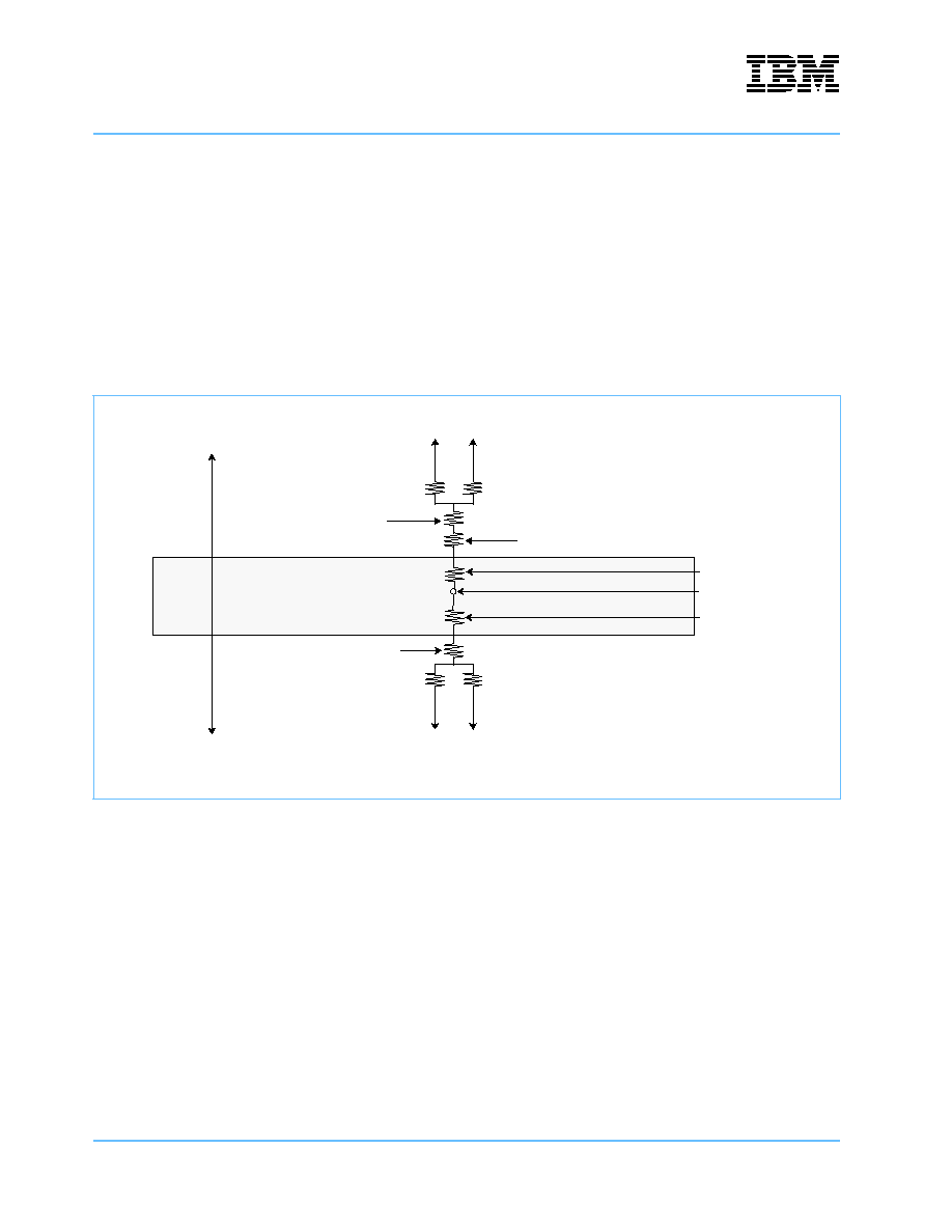
DD 2.X
PowerPC 750FX RISC Microprocessor
Preliminary
5. System Design Information
Page 52 of 63
Body_750FX_DS_DD2.X.fm.2.0
June 9, 2003
5.8.2 Internal Package Conduction
For the exposed-die packaging technology, shown in Table 3-3 Package Thermal Characteristics1 on
page 10, the intrinsic conduction thermal resistance paths are as follows.
∑ Die junction-to-case thermal resistance (Primary thermal path)
∑ Die junction-to-lead thermal resistance (Not normally a significant thermal path)
∑ Die junction-to-ambient thermal resistance (Largely dependent on customer-supplied heatsink)
Figure 5-9 depicts the primary heat transfer path for a package with an attached heat sink mounted to a
printed-circuit board.
Heat generated on the active side (ball) of the chip is conducted through the silicon, then through the heat
sink attach material (or thermal interface material), and finally to the heat sink; where it is removed by forced-
air convection. Since the silicon thermal resistance is quite small, for a first-order analysis, the temperature
drop in the silicon may be neglected. Thus, the heat sink attach material and the heat sink conduc-
tion/convective thermal resistances are the dominant terms.
The heat flow path from the die, through the chip-to-substrate balls, through the substrate, through the
substrate-to-board balls, and through the board to ambient is usually too high of a resistance to offer much
cooling. In addition, various factors make the heat flow through this path very difficult to accurately determine.
Designers must not depend on cooling the 750FX using this means unless thermal modeling has been confi-
dently completed.
Figure 5-9. C4 Package with Heat Sink Mounted to a Printed-Circuit Board
External Resistance
External Resistance
Internal
(Note the internal versus external package resistance.)
Radiation
Convection
Radiation
Convection
Heat Sink
Die/Package
Printed-Circuit Board
Thermal Interface Material
Package/Leads
Chip Junction
Resistance

DD 2.X
Preliminary
PowerPC 750FX RISC Microprocessor
Body_750FX_DS_DD2.X.fm.2.0
June 9, 2003
5. System Design Information
Page 53 of 63
5.8.3 Minimum Heat Sink Requirements
The worst-case power dissipation (PD) for the 750FX is shown in Table 3-5. A conservative thermal manage-
ment design will provide sufficient cooling to maintain the junction temperature (T
J
) of the 750FX below 105C
at maximum PD and worst-case ambient temperature and airflow conditions.
Many factors affect the 750FX power dissipation, including V
DD
, T
J
, core frequency, process factors, and the
code that is running on the processor. In general, PD increases with increases in T
J
, V
DD
, Fcore, process
variables, and the number of instructions executed per second.
For various reasons, a designer may determine that the power dissipation of the 750FX in their application
will be less than the maximum value shown in the Datasheet. Assuming a lower PD will result in a thermal
management system with less cooling capacity than would be required for the maximum Datasheet PD. In
this case, the designer may decide to determine the actual maximum 750FX PD in the particular application.
Contact your IBM PowerPC FAE for more information.
In addition to the system factors that must be considered in a cooling system analysis, three things should be
noted. First, 750FX PD rises as T
J
increases, so it is most useful to measure PD while the 750FX junction
temperature is at maximum. While not specified or guaranteed, this rise in PD with T
J
is typically less than 1W
per 10C. So regardless of other factors, the minimum cooling solution must have a maximum temperature
rise of no more than 10C/W.
This minimum cooling solution is not generally achievable without a heat sink. A heat sink or heat spreader of
some sort must always be used in 750FX applications.
Second, due to process variations, there can be a significant variation in the PD of individual 750FX devices.
In addition, IBM will occasionally supply "downbinned" parts. These are faster parts that are shipped in lieu of
the speed that was ordered. For example, some parts that are marked as 600MHz may actually run as fast as
700MHz. These 700MHz parts will dissipate more power at 600MHz than the 600MHz parts. So power dissi-
pation analysis should be conducted using the fastest parts available.
Finally, regardless of methodology, IBM only supports system designs that successfully maintain the
maximum junction temperature within Datasheet limits. IBM also supports designs that rely on the maximum
PD values given in this Datasheet, and supply a cooling solution sufficient to dissipate that amount of power
while keeping the maximum junction temperature below the maximum T
J
.

DD 2.X
PowerPC 750FX RISC Microprocessor
Preliminary
5. System Design Information
Page 54 of 63
Body_750FX_DS_DD2.X.fm.2.0
June 9, 2003
5.8.4 Heat Sink Mounting
5.8.5 Thermal Assist Unit
The thermal sensor in the Thermal Assist Unit (TAU) has not been characterized to determine the basic
uncalibrated accuracy. The relationship between the actual junction temperature and the temperature indi-
cated by THRM1 and THRM2 is not well known.
IBM recommends that the TAU in these devices be calibrated before use. Calibration methods are discussed
in the IBM Application Note Calibrating the Thermal Assist Unit in the IBM25PPC750L Processors.
Although this note was written for the 750L, the calibration methods discussed in this document also apply to
the 750FX.
In rare cases, the basic error of the TAU may be so large that a useful calibration cannot be achieved.
Figure 5-10. Package Exploded Cross-Sectional View with Several Heat Sink Options
Table 5-8. Maximum Heatsink Weight Limit for the CBGA
Force
Maximum
Maximum dynamic compressive force allowed on the BGA balls
42.9 N
Maximum dynamic tensile force allowed on the BGA balls
9.05 N
Maximum dynamic compressive force allowed on the chip
14.8 N
Maximum mass of module + heatsink when heatsink is not bolted to card
50g
CBGA Package
Heat Sink
Heat Sink clip
Adhesive
or
Thermal
Interface
Material
Printed
Option
Circuit
Board

DD 2.X
Preliminary
PowerPC 750FX RISC Microprocessor
Body_750FX_DS_DD2.X.fm.2.0
June 9, 2003
5. System Design Information
Page 55 of 63
5.8.6 Adhesives and Thermal Interface Materials
A thermal interface material is recommended at the package die-to-heat sink interface to minimize the
thermal contact resistance. For those applications where the heat sink is attached by a spring clip mecha-
nism, Figure 5-11 shows the thermal performance of three thin-sheet thermal-interface materials (silicon,
graphite/oil, floroether oil), a bare joint, and a joint with thermal grease, as a function of contact pressure. As
shown, the performance of these thermal interface materials improves with increasing contact pressure. The
use of thermal grease significantly reduces the interface thermal resistance. That is, the bare joint results in a
thermal resistance approximately seven times greater than the thermal grease joint.
In this example, the heat sink is attached to the package by means of a spring clip to holes in the printed-
circuit board (see Figure 5-10 Package Exploded Cross-Sectional View with Several Heat Sink Options on
page 54). The synthetic grease offers the best thermal performance, considering the low interface pressure.
The selection of any thermal interface material depends on many factors ≠ thermal performance require-
ments, manufacturability, service temperature, dielectric properties, cost, and so forth.
Figure 5-11. Thermal Performance of Select Thermal Interface Material
Specific Ther
mal Resistance (Kin
2
/W)
0
0.5
1
1.5
2
0
10
20
30
40
50
60
70
80
Contact Pressure (PSI)
+
+
+
Silicone Sheet (0.006 inch)
Bare Joint
Floroether Oil Sheet (0.007 inch)
Graphite/Oil Sheet (0.005 inch)
Synthetic Grease
+

DD 2.X
PowerPC 750FX RISC Microprocessor
Preliminary
5. System Design Information
Page 56 of 63
Body_750FX_DS_DD2.X.fm.2.0
June 9, 2003
5.8.7 Thermal Interface and Adhesive Vendors
The board designer can choose between several types of thermal interfaces. Heat sink adhesive materials
should be selected based upon high conductivity, yet adequate mechanical strength to meet equipment
shock/vibration requirements. A partial list of vendors that advertise thermal interface materials for PowerPC
devices is shown in Table 5-9 on page 56.
Table 5-9. 750FX Thermal Interface and Adhesive Materials Vendors
Company Names and Addresses for Thermal Interfaces and Adhesive Materials Vendors
Dow-Corning Corporation
Dow-Corning Electronic Materials
P.O. Box 0997
Midland, MI 48686-0997
(989) 496-4000
http://www.dowcorning.com/content/etronics
Chomerics, Inc.
77 Dragon Court
Woburn, MA 01888-4850
(781) 935-4850
http://www.chomerics.com
Thermagon, Inc.
4797 Detroit Avenue
Cleveland, OH 44102-2216
(216) 939-2300 / (888) 246-9050
http://www.Thermagon.com
Loctite Corporation
1001 Trout Brook Crossing
Rocky Hill, CT 06067
(860) 571-5100 / (800) 562-8483
http://www.loctite.com
AI Technology
70 Washington Road
Princeton, NJ 08550-1097
(609) 799-9388
http://www.aitechnology.com

DD 2.X
Preliminary
PowerPC 750FX RISC Microprocessor
Body_750FX_DS_DD2.X.fm.2.0
June 9, 2003
5. System Design Information
Page 57 of 63
5.8.8 Heat Sink Vendors
The board designer can choose between several types of heat sinks to place on the 750FX. A partial list of
vendors that advertise heat sinks for Power PC devices is shown in Table 5-10 A Partial Listing of 750FX
Heat Sink Vendors on page 57.
Table 5-10.
A Partial Listing of
750FX Heat Sink Vendors
Company Names and Addresses for Heat Sink Vendors
Chip Coolers, Inc.
333 Strawberry Field Rd.
Warwick, RI 02886
(800) 227-0254
http://www.chipcoolers.com
International Electronic Research Corporation (IERC)
413 North Moss Street
Burbank, CA 91502
(818) 842-7277
http://www.ctscorp.com/ierc
Aavid Thermalloy
80 Commercial Street
Concord, NH 03301
(603) 224-9888
http://www.aavid.com
http://www.aavidthermalloy.com
Wakefield Thermal Solutions Inc.
33 Bridge Street
Pellham, NH 03076
(603) 635-2800
http://www.wakefield.com

DD 2.X
PowerPC 750FX RISC Microprocessor
Preliminary
5. System Design Information
Page 58 of 63
Body_750FX_DS_DD2.X.fm.2.0
June 9, 2003

DD2.X
Preliminary
PowerPC 750FX RISC Microprocessor
Rev_Log_750FX_DS_DD2.X.fm.2.0
June 9, 2003
Revision Log
Page 59 of 59
Revision Log
Date
Description
Feb 13, 2003
Version 0.1
Initial preliminary version for general release of 750FX DD2.3.
May 16, 2003
Version 1.0
Second preliminary version which includes input/updates from designers.
May 23, 2003
Version 2.0
Third preliminary version which includes input/updates from designers.
June 3, 2003
Version 2.0
Fourth preliminary version which includes input/updates from designers.
June 5, 2003
Version 2.0
Changed from DD2.3 to DD2.X. Also included designer updates.
June 6, 2003
Version 2.0
Changed Table 3-5 Power Consumption.
June 9, 2003
Version 2.0
Removed Rev bars..
