
PRELIMINARY
�
�
�
�
D
O
IF
D
O
RF
f
IN
IF
�
�
!"
�
!�
#$%
�
f
IN
RF
HM6P5331
HM6P5331 � 2.0GHz/500MHz Dual Frequency Synthesizer
Features
Full CMOS RF frequency synthesizer
Low Current Consumption
Selectable Powersave Mode
Dual Modulus Prescaler
Selectable Charge Pump High Z State
2.7V to 3.6V Operation
Small Out Line 20 Pin TSSOP Package
24 Pin LGA(Leadless Grid Array) Package
Applications
Portable Wireless Communications
Cordless and Cellular Telephone Systems
Wireless Local Area Networks(WLANs)
Cable TV Tuners(CATV)
Other Wireless Communication Systems
Description
The
HM6P5331 of full CMOS monolithic,
dual
frequency
synthesizer is to be used as a local oscillator for RF and IF
of a dual conversion transceiver. It is fabricated using
Hyundai's standard CMOS process.
HM6P5331 contains dual modulus prescalers. A 64/65 or
a 128/129 prescaler can be selected for RF synthesizer
and a 8/9 or 16/17 prescaler can be selected for IF
synthesizer. Using digital phase locked loop technique,
HM6P5331 provides the tuning voltage for voltage
controlled oscillators to generate very stable low noise RF
& IF local oscillator signals. Serial data is transferred into
the HM6P5331 via three wire interface (Data, Enable,
Clock). Supply voltage can range from 2.7 to 3.6 V.
HM6P5331 features very low current consumption; 4.4mA
at 3.0V.
HM6P5331 is available in a TSSOP 20-pin, LGA(Leadless
Grid Array) 24-pin surface mount plastic package.
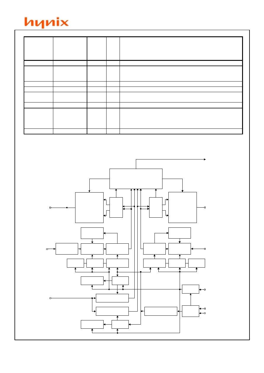
Functional Block Diagram
PRELIMINARY
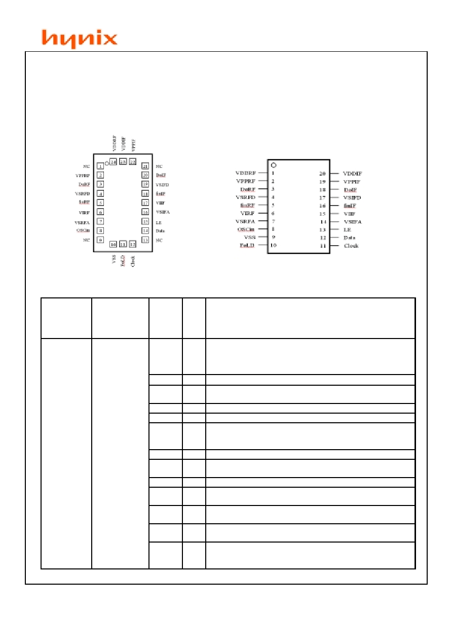
Pin Assignment
Pin Description
Leadless Grid Array Package Thin Shrink Small Outline Package TM
Pin No.
HM6C5332
24-pin LGA
Package
Pin No.
HM6C5332
20-pin TSSOP
Package
PIN
NAME
I/O
Description
24
1
VDDRF
-
Power supply voltage input for RF analog and RF digital circuits. Input may
range from 2.7V to 3.6V. VDDRF must equal VDDIF. Bypass capacitors
should be placed as close as possible to this pin and be connected directly
to the ground plane.
2
2
VPPRF
-
Power Supply for RF charge pump. Must be
VDDRF.
3
3
DoRF
O
Internal RF charge pump output. For connection to a loop filter for driving
the input of an external VCO.
4
4
VSRFD
-
Ground for RF digital circuitry.
5
5
finRF
I
RF prescaler input. Small signal input from the VCO.
6
6
VIRF
-
This pin is to provide a bypass capacitor to the internal voltage supply and
bypass capacitor must be placed between this pin and RF analog GND(Pin
7). With a slight performance degradation, this pin may be NC.
7
7
VSRFA
-
Ground for RF analog circuitry.
8
8
OSCin
I
Oscillator input. The input has a VDDRF/2 input threshold and can be
driven from an external CMOS or TTL logic gate.
10
9
VSS
-
Ground for data interface, FoLD, and oscillator circuits.
11
10
FoLD
O
Multiplexed output of the RF/IF programmable or reference dividers, and
RF/IF lock detect signals. CMOS output(See Programmable Modes)
12
11
Clock
I
High impedance CMOS Clock input. Data for the various counters is
clocked in on the rising edge, into the 22-bit shift register.
14
12
Data
I
Binary serial data input. Data entered MSB first. The last two bits are the
control bits. High impedance CMOS input.
15
13
LE
I
Load enable high impedance CMOS input. When LE goes HIGH, data
stored in the shift register is loaded into one of the 4 appropriate
latches(control bit dependent).
PRELIMINARY
Pin No.
HM6C5332
24-pin LGA
Package
Pin No.
HM6C5332
20-pin TSSOP
Package
PIN
NAME
I/O
Description
16
14
VSIFA
-
Ground for IF analog circuitry.
17
15
VIIF
-
This pin is to provide a bypass capacitor to the internal voltage supply and
bypass capacitor must be placed between this pin and IF analog GND(Pin
14). With a slight performance degradation, this pin may be NC.
18
16
finIF
I
IF prescaler input. Small signal input from the VCO.
19
17
VSIFD
-
Ground for IF digital circuitry.
20
18
DoIF
O
Internal IF charge pump output. For connection to a loop filter for driving
the input of an external VCO.
22
19
VPPIF
-
Power Supply for IF charge pump. Must be
VDDIF.
23
20
VDDIF
-
Power supply voltage input for IF analog, IF digital, data interface, FoLD,
and oscillator circuits. Input may range from 2.7V to 3.6V. VDDIF must
equal VDDRF. Bypass capacitors should be placed as close as possible to
this pin and be connected directly to the ground plane.
1,9,13,21
X
NC
-
No Connect
Block Diagram
�
OSCin
Clock
Data
LE
DoIF
DoRF
finIF
finRF
�
�
!�
�
!"#
!
��$
!
��$
!�
�
!"#
�
%
&
'
�
($$
�
'
�
(
$�'
!)
)
!
)
'
)
)
(
#
)
%
&
'
%
"(*
FoLD
+,+
+,+
PRELIMINARY
Absolute Maximum Ratings
Power Supply Voltage
VDD -0.3V to +4.2V
VPP -0.3V to +4.2V
Voltage on Any Pin
with GND = 0V (V
I
) -0.3V to +4.2V
Storage Temperature Range (T
S
) -65
�
C to +150
�
C
Lead Temperature (solder 4 sec.) (T
L
) 260
�
C
Thermal Resistance(Typical)
JA
(
�
C/W)
TSSOP Package 130
�
C
Operating Conditions
Power Supply Voltage
VDD 2.7V to 3.6V
VPP VDD to 3.6V
Operating Temperature(T
A
) -40
�
C to 85
�
C
CAUTION: Stress above those listed in "Absolute Maximum Ratings" may cause permanent damage to the device. Other conditions
above those indicated in the operational sections of this specification are not implied.
Electrical Characteristics
V
DD
= 3.0V, -40
�
C < T
A
< 85
�
C, Except as Specified
Symbol
Parameter
Conditions
Min
Typ
Max
Units
RF
V
DD
=2.7V to 3.6V,
f
= 10KHz
3.2
mA
I
DD
Power Supply Current
IF
V
DD
=2.7V to 3.6V,
f
= 10KHz
1.2
5.4
mA
I
DD-PWDN
Powerdown Current
V
DD
=3.0V
1
10
�
A
f
IN
RF
Operating Frequency
0.5
-
2.0
GHz
f
IN
IF
Operating Frequency
50
-
500
MHz
f
OSC
Oscillator Frequency.
4
-
40
MHz
f
Maximum Phase Detector Freq.
10
-
-
MHz
Pf
IN
RF
RF Input Sensitivity
V
DD
=2.7V to 3.6V
- 8.5
-
0
dBm
Pf
IN
IF
IF Input Sensitivity
V
DD
=2.7V to 3.6V
-10
-
0
dBm
V
OSC
Oscillator Sensitivity
OSC
IN
0.5
-
-
V
PP
V
IH
High Level Input Voltage
*
0.8 V
DD
-
-
V
V
IL
Low Level Input Voltage
*
-
-
0.2 V
DD
V
I
IH
High Level Input Current
V
IH
=V
DD
=3.6V*
-1.0
-
1.0
�
A
I
IL
Low Level Input Current
V
IL
=0V, V
DD
=3.6V*
-1.0
-
1.0
�
A
I
IH
Oscillator Input Current
V
IH
=V
DD
=3.6V
-
-
100
�
A
I
IL
Oscillator Input Current
V
IL
=0V, V
DD
=3.6V
-100
-
-
�
A
V
OH
High-Level Output Voltage
I
OH
= -500
�
A
V
DD
-0.4
-
-
V
V
OL
Low-Level Output Voltage
I
OL
= 500
�
A
-
-
0.4
V
t
CS
Data Clock Setup Time
See Data Input Timing
50
-
-
ns
t
CH
Data Clock Hold Time
See Data Input Timing
10
-
t
CWH
Clock Pulse Width High
See Data Input Timing
50
-
-
t
CWL
Clock Pulse Width Low
See Data Input Timing
50
-
-
t
ES
Clock to Load Enable Setup Time
See Data Input Timing
50
-
-
t
EW
Load Enable Pulse Width
See Data Input Timing
50
-
-
* Clock, Data and LE. Does not include f
IN
RF, f
IN
IF and OSC
IN
.
PRELIMINARY
�
�
�
�
D
O
IF
D
O
RF
f
IN
IF
�
�
!"
�
!�
#$%
�
f
IN
RF
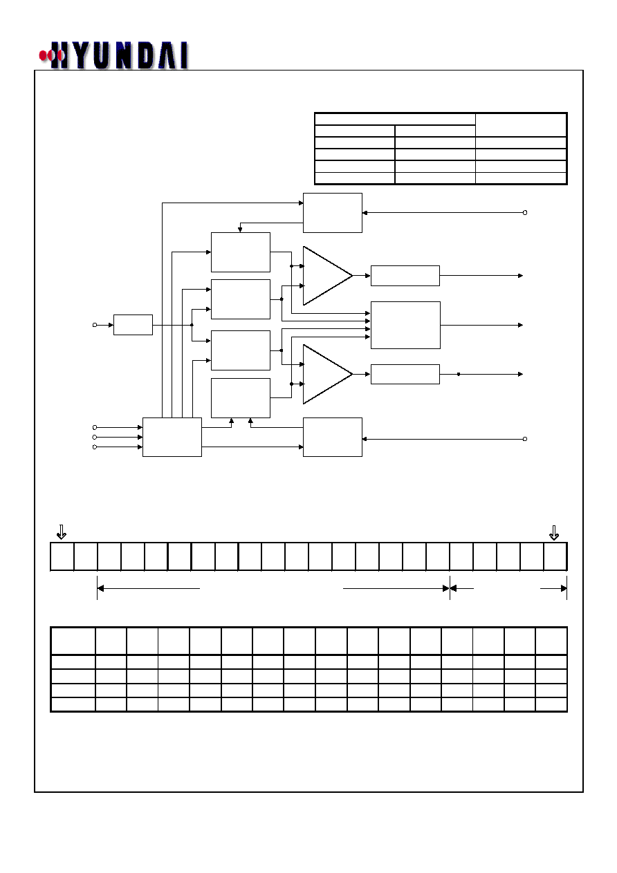
Functional Description
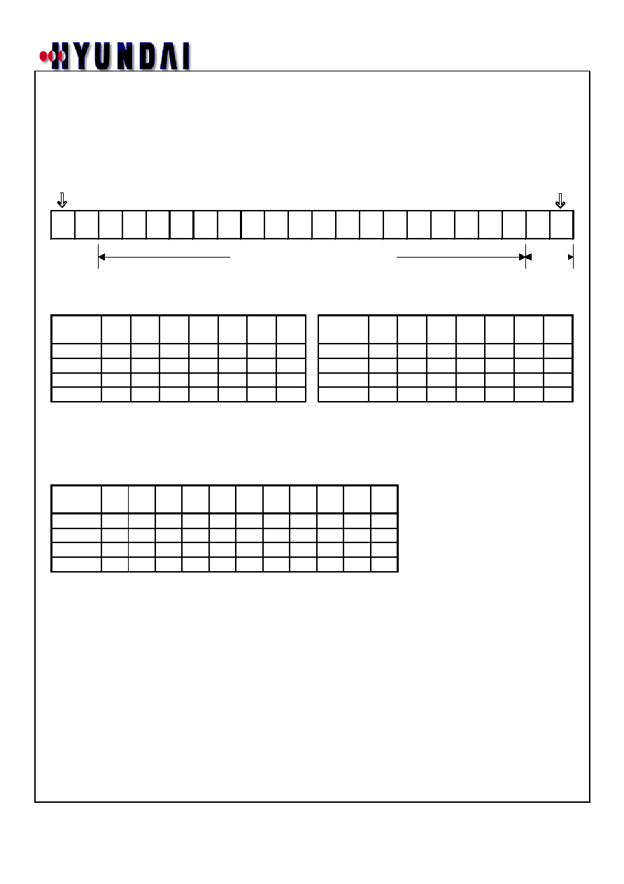
The simplified block diagram below shows the 22-bit data
register, two 15-bit R Counters and the 15-bit and 18-bit N
Counters (intermediate latches are not shown). The data
stream is clocked (on the rising edge of Clock) into the
DATA input, MSB first. The last two bits are the Control
Bits. The DATA is transferred into the counters as follows:
CONTROL BITS
C1
C2
DATA LOCATION
0
0
IF R Counter
0
1
RF R Counter
1
0
IF N Counter
1
1
RF N Counter
Programmable Reference Dividers (IF and RF R Counters)
If the Control Bits are 00 or 01 (00 for IF and 01 for RF) data is transferred from the 22bit shift register into a latch which
sets the 15-bit R Counter. Serial data format is shown below.
15-Bit Programmable Reference Divider Ratio (R Counter)
DIVIDE
R
R
R
R
R
R
R
R
R
R
R
R
R
R
R
RATIO
15
14
13
12
11
10
9
8
7
6
5
4
3
2
1
3
0
0
0
0
0
0
0
0
0
0
0
0
0
1
1
4
0
0
0
0
0
0
0
0
0
0
0
0
1
0
0
�
�
�
�
�
�
�
�
�
�
�
�
�
�
�
�
32767
1
1
1
1
1
1
1
1
1
1
1
1
1
1
1
NOTES:
1. Divide ratios less than 3 are prohibited.
2. Divide ratio: 3 to 32767.
3. R1 to R15: These bits select the divide ratio of the programmable reference divider.
4. Data is shifted in MSB first.
�
�
�
PRELIMINARY
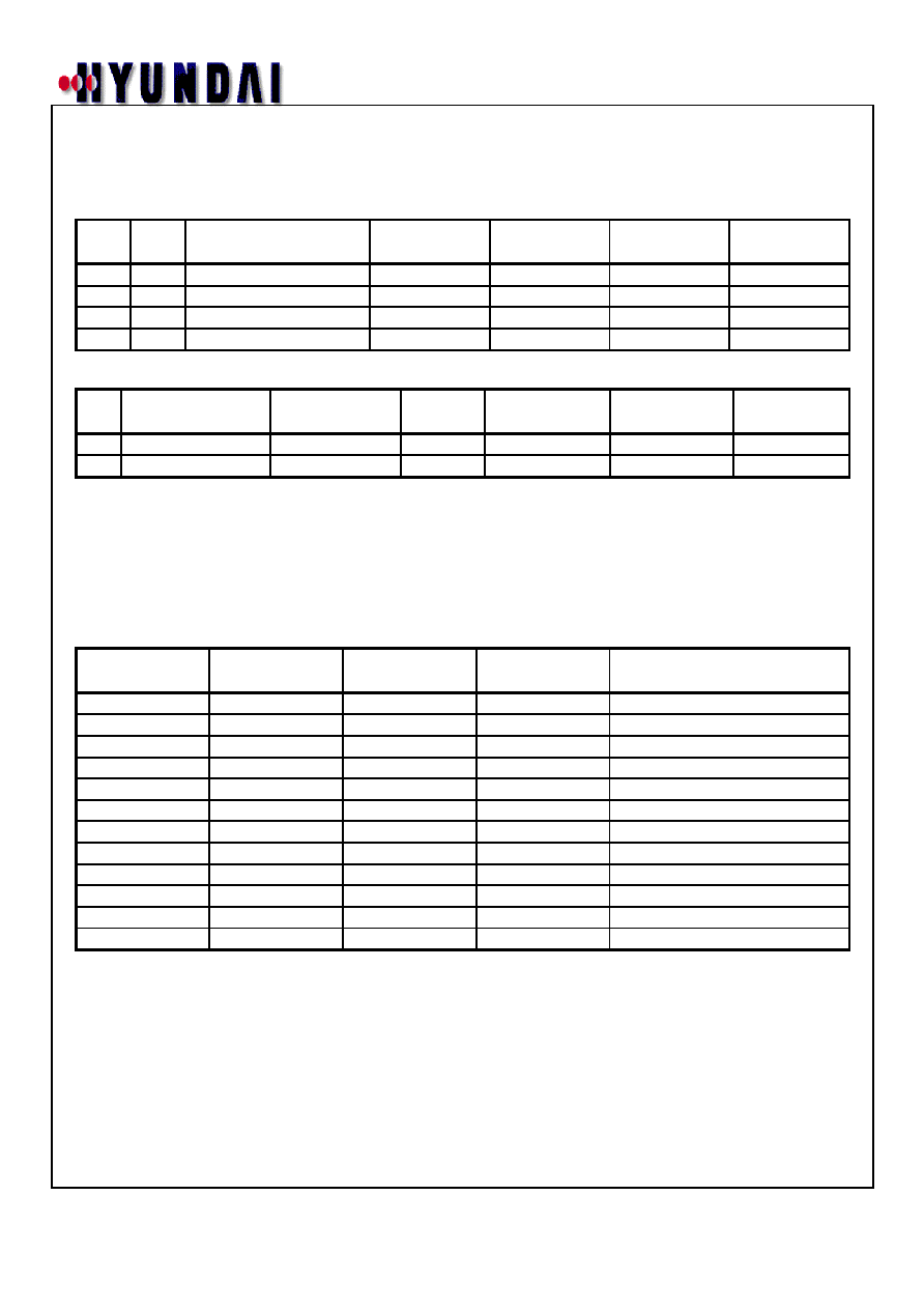
Programmable Divide (N Counter)
The N counter consists of the 7-bit swallow counter (A counter) and the 11-bit programmable counter (B counter). If the
Control Bits are 10 or 11 (10 for IF counter and 11 for RF counter) data is transferred from the 22-bit shift register into a 4-
bit or 7-bit latch (which sets the Swallow (A) Counter) and an 11-bit latch (which sets the 11-bit programmable (B) Counter),
MSB first. Serial data format is shown below. For the IF N counter bits 5, 6, and 7 are don't care bits. The RF N counter
does not have don't care bits.
7-Bit Swallow Counter Divide Ratio (A Counter)
RF
DIVIDE
N
N
N
N
N
N
N
RATIO A
7
6
5
4
3
2
1
0
0
0
0
0
0
0
0
1
0
0
0
0
0
0
1
�
�
�
�
�
�
�
�
127
1
1
1
1
1
1
1
NOTES:
1. Divide ratio 0 to 127
2. B
A
IF
DIVIDE
N
N
N
N
N
N
N
RATIO A
7
6
5
4
3
2
1
0
X
X
X
0
0
0
0
1
X
X
X
0
0
0
1
�
�
�
�
�
�
�
�
15
X
X
X
1
1
1
1
X = Don't care condition
11-Bit Programmable Counter Divide Ratio (B Counter)
DIVIDE
N
N
N
N
N
N
N
N
N
N
N
RATIO A
18
17
16
15
14
13
12
11
10
9
8
3
0
0
0
0
0
0
0
0
0
1
1
4
0
0
0
0
0
0
0
0
1
0
0
�
�
�
�
�
�
�
�
�
�
�
�
2047
1
1
1
1
1
1
1
1
1
1
1
NOTES:
1. Divide ratio 3 to 2047 (divide ratios less than 3 are prohibited).
2. B
A
Pulse Swallow Function
f
VCO
= [(P
B) + A]
f
OSC
/R
f
VCO
: Output frequency of external voltage controlled oscillator (VCO)
B:
Preset divide ratio of binary 11-bit programmable counter (3 to 2047)
A:
Preset divide ratio of binary 7-bit swallow counter (0
A
127 {RF}, 0
A
15 {IF}, A
B)
f
OSC
: Output frequency of the external reference frequency oscillator
R:
Preset divide ratio of binary 15-bit programmable reference counter (3 to 32767)
P:
Preset modulus of dual modulus prescaler (for IF: P=8 or 16; for RF: P=64 or 128)
�
�
!"#$!%
PRELIMINARY
Programmable Modes
Several modes of operation can be programmed with bits R16-R18 including the phase detector polarity and charge pump
High Z State. The prescaler and powerdown modes are selected with bits N19 and N20. The programmable modes and
truth table for the programmable modes are shown below.
C1
C2
R16
R17
R18
R19
R20
0
0
IF Phase Detector Polarity
IF I
CPO
IF D
O
High Z
IF LD
IF F
O
0
1
RF Phase Detector Polarity
RF I
CPO
RF D
O
High Z
RF LD
RF F
O
1
0
-
-
-
IF Prescaler
Powerdown IF
1
1
-
-
-
RF Prescaler
Powerdown RF
Mode Select Truth Table
PHASE DETECTOR
POLARITY
D
O
High Z STATE
I
CPO
(NOTE 1)
IF PRESCALER
RF
PRESCALER
POWERDOWN
(NOTE 2)
0
Negative
Normal Operation
LOW
8/9
64/65
Powered Up
1
Positive
High Z State
HIGH
16/17
128/129
Powered Down
NOTES:
1. Activation of the IF PLL or RF PLL powerdown modes result in the disabling of the respective N counter divider and
debiasing of its respective f
IN
inputs (to a high impedance state). Powerdown forces the respective charge pump and
phase comparator logic to a High Z State condition. The R counter functionality does not become disabled until both IF
and RF powerdown bits are activated. The OSC
IN
pin reverts to a high impedance state when this condition exists. The
control register remains active and capable of loading and latching in data during all the powerdown modes.
F
O
LD (Pin 10) Output Truth Table
RF R[19]
(RF LD)
IF R[19]
(IF LD)
RF R[20]
(RF F
O
)
IF R[20]
(IF F
O
)
F
O
OUTPUT STATE
0
0
0
0
Disabled (Note1)
0
1
0
0
IF Lock Detect (Note2)
1
0
0
0
RF Lock Detect (Note2)
1
1
0
0
RF/IF Lock Detect (Note2)
X
0
0
1
IF Reference Divider Output
X
0
1
0
RF Reference Divider Output
X
1
0
1
IF Programmable Divider Output
X
1
1
0
RF Programmable Divider Output
0
0
1
1
For Internal Use Only
0
1
1
1
For Internal Use Only
1
0
1
1
For Internal Use Only
1
1
1
1
Counter Reset (Note4)
X = don't care condition
NOTES:
1. When the F
O
LD output is disabled, it is actively pulled to a low logic state.
2. Lock detect output provided to indicate when the VCO frequency is in "lock". When the loop is locked and a lock detect mode is
selected, the pins output is HIGH, with narrow pulse LOW. In the RF/IF lock detect mode a locked condition is indicated when RF and
IF are both locked.
3. The Counter Reset mode bits R19 and R20 when activated reset all counters. Upon removal of the Reset bits then N counter resumes
counting in "close" alignment with the R counter. (The maximum error is one prescaler cycle). If the Reset bits are activated the R
counter is also forced to Reset, allowing smooth acquisition upon powering up.
PRELIMINARY
�
Phase Detector Polarity
Depending upon VCO characteristics, R16 bit should be
set accordingly:
When VCO characteristics are positive like (1), R16
should be set HIGH; When VCO characteristics are
negative like (2), R16 should be set LOW.
��
�
�
Serial Data Input Timing
&'&
()*
(+
(+
)
�,-.
�
,(-.
�,-.
�
,(-.
NOTES:
1. Parenthesis data indicates programmable reference divider data.
2. Data shifted into register on clock rising edge.
3. Data is shifted in MSB first.
Test Conditions: The Serial Data Input Timing is tested using a symmetrical waveform around V
DD
/2. The test waveform
has an edge rate of 0.6V/ns with amplitudes of 2.2V at V
DD
= 2.7V and 2.6V at V
DD
= 3.6V.
Phase Comparator and Internal Charge Pump Characteristics
"
(
"
"
/"
"
0"
"
1"
"
1"
"
1"
NOTES:
1. Phase difference detection range: -2
to +2
2. The minimum width pump up and pump down current pulse occur at the D
O
pin when the loop is locked.
3. R16 = HIGH
PRELIMINARY
Powerdown Operation
Synchronous and asynchronous powerdown modes are both available. Synchronously powerdown occurs if the respective
loop's R18 bit (Do High Z State) is LOW when its N20 bit (Powerdown) becomes HI. Asynchronous powerdown occurs if
the loop's R18 bit is HI when its N20 bit becomes HI. In the synchronous powerdown mode, the powerdown function is
gated by the charge pump to prevent unwanted frequency jumps. Once the powerdown program bit N20 is loaded, the
part will go into powerdown mode when the charge pump reaches a High Z condition. In the asynchronous powerdown
mode, the device powers down immediately after the LE pin latches in a HI condition on the powerdown bit N20. Activation
of either the IF or RF PLL powerdown conditions in either synchronous or asynchronous modes forces the respective
loop's R and N dividers to their load state condition and debiasing of its respective fin input to a high impedance state. The
oscillator circuitry function does not become disabled until both IF and RF powerdown bits are activated. The control
register remains active and capable of loading and latching data during all of the powerdown modes. The device returns to
an actively powered up condition in either synchronous or asynchronous modes immediately upon LE latching LOW data
into bit N20.
Powerdown Mode Select Table
R18
N20
Powerdown Status
0
0
PLL Active
1
0
PLL Active (Charge Pump High Z State)
0
1
Synchronous Powerdown Initiated
1
1
Asynchronous Powerdown Initiated
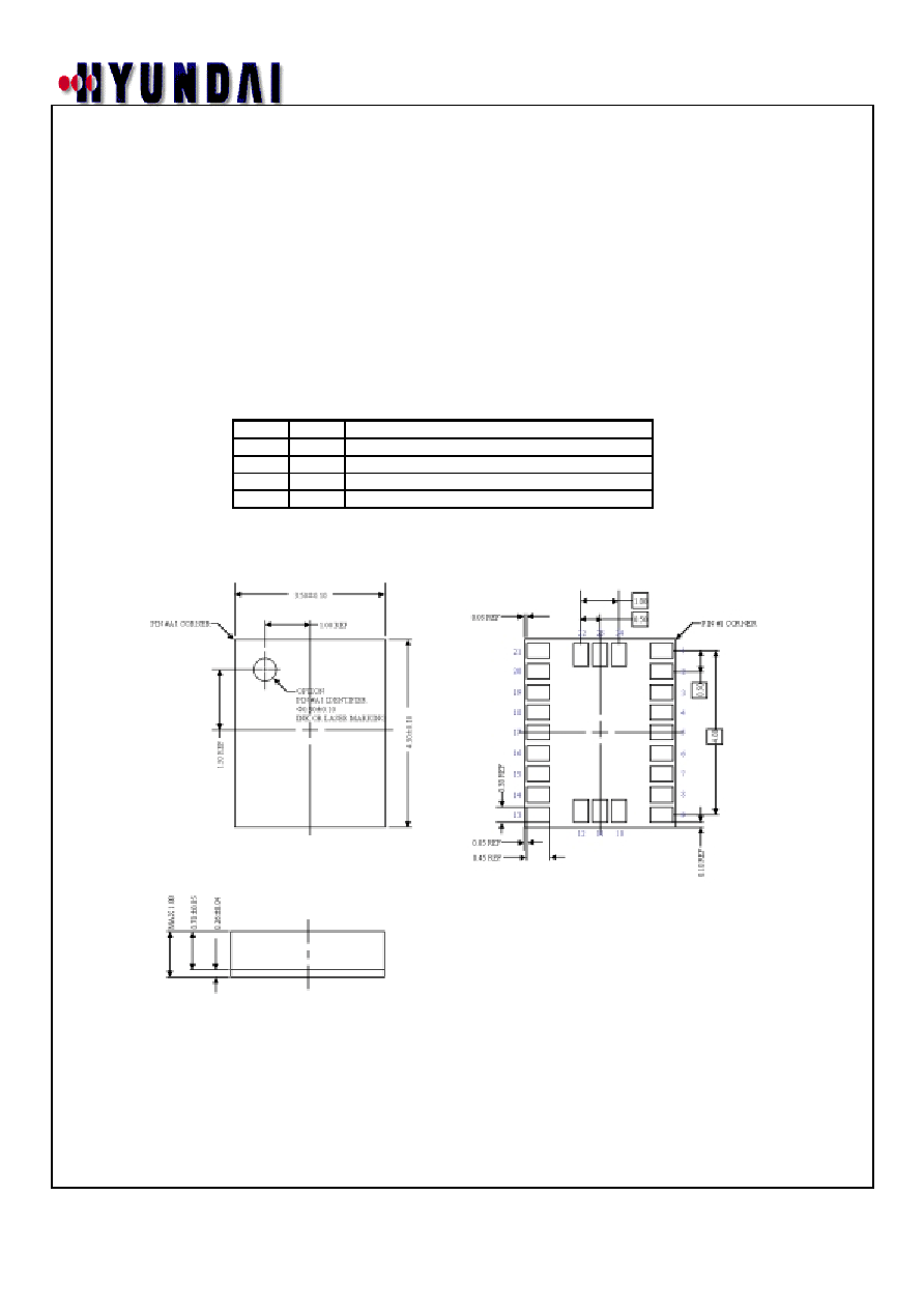
Physical Dimensions
(unit :
)
Leadless Grid Array Package
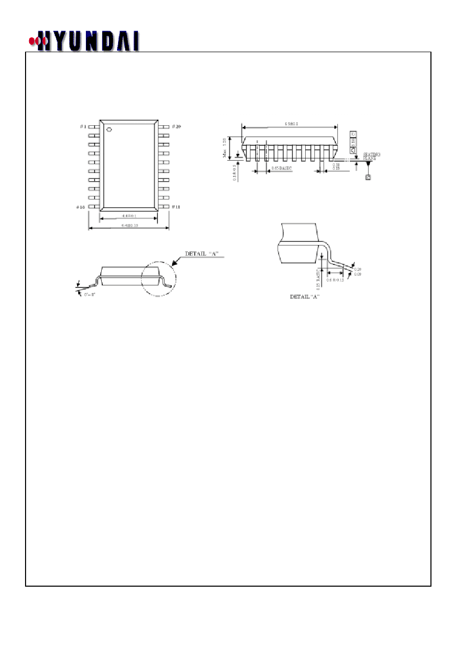
PRELIMINARY
Physical Dimensions continued (unit :
)
Thin Shrink Small Outline Package