Äîêóìåíòàöèÿ è îïèñàíèÿ www.docs.chipfind.ru

16/32 BIT RISC/DSP
GMS30C2216
GMS30C2232
USER'S MANUAL
Jun. 29, 2001 Ver. 3.1

Revision 3.1
Published by
IDA Team in Hynix Semiconductor Inc.
¨ Ï
Hynix Semiconductor 2001. All Right Reserved.
Hynix Offices in Korea or Distributors and Representatives listed at address directory may
serve additional information of this manual.
Hynix reserves the right to make changes to any Information here in at any time without
notice.
The information, diagrams, and other data in this manual are correct and reliable;
however, Hynix is in no way responsible for any violations of patents or other rights of
the third party generated by the use of this manual.

Specifications and information in this document are subject to change without notice and do
not represent a commitment on the part of Hynix. Hynix reserves the right to make changes
to improve functioning. Although the information in this document has been carefully
reviewed, Hynix does not assume any liability arising out of the use of the product or circuit
described herein.
Hynix does not authorize the use of the Hynix microprocessor in life support applications
wherein a failure or malfunction of the microprocessor may directly threaten life or cause
injury. The user of the Hynix microprocessor in life support applications assumes all risks of
such use and indemnifies Hynix against all damages.
For further information please contact:
SEOUL OFFICE : Hynix YOUNG DONG Bldg.
891, Daechi-dong, Kangnam-gu,
Seoul, Korea.
PHONE : (02) 3459-3662~3
FAX : (02) 3459-3942
SYSTEM IC : 1, Hyangjeong-dong, Hungduk-gu,
Cheongju, 361-725, Korea.
PHONE : (0431) 270-4030~47
FAX : (0431) 270-4075
©
Copyright 2001Hynix Semiconductor Inc.
Revision Jun. 29, 2001.


Table of Contents i
Table of Contents
0. Overview
0.1 GMS30C2216/32 RISC/DSP.............................................................................. 0-1
0.2 Block Diagram .................................................................................................... 0-8
0.3 Pin Configuration................................................................................................ 0-9
0.3.1 GMS30C2232, 160-Pin MQFP-Package - View from Top Side ........ 0-9
0.3.2 Pin Cross Reference by Pin Name .................................................... 0-10
0.3.2 Pin Cross Reference by Location ...................................................... 0-11
0.3.4 Pin Fuction ........................................................................................ 0-12
1.
Architecture
1.1 Introduction...................................................................................................... 1-1
1.1.1 RISC Architecture ............................................................................... 1-1
1.1.2 Techniques to reduce CPI (Cycles per Instruction)............................. 1-2
1.1.3 The pipeline structure of GMS30C2232 ............................................. 1-7
1.2 Global Register Set .......................................................................................... 1-8
1.2.1 Program Counter PC, G0 .................................................................... 1-9
1.2.2 Status Register SR, G1 ...................................................................... 1-10
1.2.3 Floating-Point Exception Register FER, G2 ..................................... 1-13
1.2.4 Stack Pointer SP, G18 ....................................................................... 1-14
1.2.5 Upper Stack Bound UB, G19 ............................................................ 1-14
1.2.6 Bus Control Register BCR, G20 ....................................................... 1-14
1.2.7 Timer Prescaler Register TPR, G21 .................................................. 1-15
1.2.8 Timer Compare Register TCR, G22.................................................. 1-15
1.2.9 Timer Register TR, G23.................................................................... 1-15
1.2.10 Watchdog Compare Register WCR, G24........................................ 1-15
1.2.11 Input Status Register ISR, G25 ....................................................... 1-15
1.2.12 Function Control Register FCR, G26.............................................. 1-15
1.2.13 Memory Control Register MCR, G27............................................. 1-16
1.3 Local Register Set .......................................................................................... 1-16
1.4 Privilege States .............................................................................................. 1-17
1.5 Register Data Types....................................................................................... 1-18
1.6 Memory Organization.................................................................................... 1-19
1.7 Stack............................................................................................................... 1-21
1.8 Instruction Cache ........................................................................................... 1-26
1.9 On-Chip Memory (IRAM)............................................................................. 1-29

ii TABLE of Contents
2. Instructions General
2.1 Instruction Notation..........................................................................................2-1
2.2 Instruction Execution........................................................................................2-2
2.3 Instruction Formats...........................................................................................2-3
2.3.1 Table of Immediate Values ..................................................................2-5
2.3.2 Table of Instruction Codes ...................................................................2-6
2.3.3 Table of Extended DSP Instruction Codes ..........................................2-7
2.4 Entry Tables......................................................................................................2-8
2.5 Instruction Timing ..........................................................................................2-12
3. Instruction Set
3.1 Memory Instructions ........................................................................................3-1
3.1.1 Address Modes.....................................................................................3-2
3.1.2 Load Instructions..................................................................................3-7
3.1.3 Store Instructions ...............................................................................3-10
3.2 Move Word Instructions.................................................................................3-13
3.3 Move Double-Word Instruction .....................................................................3-13
3.4 Logical Instructions ........................................................................................3-15
3.5 Invert Instruction ............................................................................................3-16
3.6 Mask Instruction .............................................................................................3-16
3.7 Add Instructions .............................................................................................3-17
3.8 Sum Instructions .............................................................................................3-19
3.9 Subtract Instructions .......................................................................................3-20
3.10 Negate Instructions .......................................................................................3-21
3.11 Multiply Word Instruction............................................................................3-22
3.12 Multiply Double-Word Instructions .............................................................3-22
3.13 Divide Instructions .......................................................................................3-24
3.14 Shift Left Instructions...................................................................................3-26
3.15 Shift Right Instructions.................................................................................3-27
3.16 Rotate Left Instruction..................................................................................3-29
3.17 Index Move Instructions...............................................................................3-20
3.18 Check Instructions ........................................................................................3-32
3.19 No Operation Instruction ..............................................................................3-32
3.20 Compare Instructions....................................................................................3-33
3.21 Compare Bit Instructions..............................................................................3-34
3.22 Test Leading Zeros Instruction.....................................................................3-34
3.23 Set Stack Address Instruction.......................................................................3-35
3.24 Set Conditional Instructions .........................................................................3-35
3.25 Branch Instructions.......................................................................................3-37
3.26 Delayed Branch Instructions ........................................................................3-39

Table of Contents iii
3.27 Call Instruction ............................................................................................ 3-41
3.28 Trap Instructions .......................................................................................... 3-43
3.29 Frame Instruction ......................................................................................... 3-45
3.30 Return Instruction ........................................................................................ 3-48
3.31 Fetch Instruction .......................................................................................... 3-50
3.32 Extended DSP Instructions .......................................................................... 3-51
3.33 Software Instructions ................................................................................... 3-54
3.33.1 Do Instruction.................................................................................. 3-55
3.33.2 Floating-Point Instructions .............................................................. 3-56
4. Exceptions
4.1 Exception Processing....................................................................................... 4-1
4.2 Exception Types .............................................................................................. 4-2
4.2.1 Reset .................................................................................................... 4-2
4.2.2 Range, Pointer, Frame and Privilege Error ......................................... 4-2
4.2.3 Extended Overflow.............................................................................. 4-3
4.2.4 Parity Error .......................................................................................... 4-3
4.2.5 Interrupt ............................................................................................... 4-3
4.2.6 Trace Exception................................................................................... 4-4
4.3 Exception Backtracking................................................................................... 4-4
5. Timer and CPU clock Modes
5.1 Overview.......................................................................................................... 5-1
5.1.1 Timer Prescaler Register TPR............................................................. 5-1
5.1.2 Timer Register TR............................................................................... 5-2
5.1.3 Timer Compare Register TCR ............................................................ 5-3
5.1.4 Power-Down Mode ............................................................................. 5-3
5.1.5 Additional Power Saving..................................................................... 5-4
5.1.6 Sleep Mode.......................................................................................... 5-5

iv TABLE of Contents
6. Bus Interface
6.1 Bus Control General .........................................................................................6-1
6.1.1 Boot Width Selection ...........................................................................6-2
6.1.2 SRAM and ROM Bus Access ..............................................................6-2
6.1.3 DRAM Bus Access ..............................................................................6-3
6.1.3.1 DRAM Row Address Bits Multiplexing.............................6-4
6.2 I/O Bus Control ................................................................................................6-5
6.2.1 I/O Bus Control....................................................................................6-6
6.3 Bus Control Register BCR ...............................................................................6-7
6.4 Memory Control Register MCR .....................................................................6-11
6.4.1 MEMx Parity Disable ........................................................................6-13
6.4.2 MEMx Wait Disable ..........................................................................6-13
6.4.3 MEMx Byte Mode .............................................................................6-13
6.4.4 Power Down.......................................................................................6-13
6.4.5 IRAM Refresh Test ............................................................................6-14
6.4.6 IRAM Refresh Rate ...........................................................................6-14
6.4.7 DRAM Type ......................................................................................6-14
6.4.8 Entry Table Map ................................................................................6-14
6.4.10 MEMx Bus Size ...............................................................................6-14
6.5 Input Status Register ISR ...............................................................................6-15
6.6 Function Control Register FCR......................................................................6-16
6.7 Watchdog Compare Register WCR................................................................6-18
6.8 IO3 Control Modes.........................................................................................6-18
6.8.1 IO3Standard Mode .............................................................................6-18
6.8.2 Watchdog Mode .................................................................................6-18
6.8.3 IO3Timing Mode ...............................................................................6-19
6.8.4 IO3TimerInterrupt Mode ...................................................................6-19
6.9 Bus Signals .....................................................................................................6-20
6.9.1 Bus Signals for the GMS30C2232 Processor ....................................6-20
6.9.2 Bus Signals for the GMS30C2216 Processor ....................................6-21
6.9.3 Bus Signal Description.......................................................................6-22
6.10 Bus Cycles ....................................................................................................6-27
6.10.1 MEMx Byte Mode =1 ......................................................................6-27
6.10.1.1 SRAM and ROM Single-Cycle Read Access.................6-27
6.10.1.2 SRAM and ROM Single-Cycle Write Access ................6-27
6.10.1.3 SRAM and ROM Multi-Cycle Read Access ..................6-28
6.10.1.4 SRAM Multi-Cycle Write Access ..................................6-28
6.10.2 MEMx Byte Mode =0 ......................................................................6-29
6.10.2.1 SRAM Single-Cycle Read Access ..................................6-29
6.10.2.2 SRAM Single-Cycle Write Access.................................6-29
6.10.2.3 SRAM Multi-Cycle Read Access ...................................6-30

Table of Contents v
6.10.2.4 SRAM Multi-Cycle Write Access ................................. 6-30
6.10.3 MEM2 Read Access with WAIT Pin .............................................. 6-31
6.10.4 I/O Read Access .............................................................................. 6-32
6.10.5 I/O Read Access with WAIT Pin .................................................... 6-33
6.10.6 I/O Write Access ............................................................................. 6-34
6.10.7 DRAM............................................................................................. 6-35
6.10.7.1 Fast Page Mode DRAM Access ..................................... 6-35
6.10.7.2 EDO DRAM Single-Cycle Access................................. 6-36
6.10.7.3 EDO DRAM Multi-Cycle Access .................................. 6-37
6.10.7.4 DRAM Refresh(CAS Before RAS Refresh.................... 6-38
6.10 DC Characteristics ....................................................................................... 6-39
7. Mechanical Data
7.1 GMS30C2232, 160-Pin MQFP-Package ....................................................... 7-1
7.1.1 Pin Configuration - View from Top Side............................................ 7-1
7.1.2 Pin Cross Reference by Pin Name ...................................................... 7-2
7.1.3 Pin Cross Reference by Location ........................................................ 7-3
7.2 GMS30C2232, 144-Pin TQFP-Package ........................................................ 7-4
7.2.1 Pin Configuration - View from Top Side............................................ 7-4
7.2.2 Pin Cross Reference by Pin Name ...................................................... 7-5
7.2.3 Pin Cross Reference by Location ........................................................ 7-6
7.3 GMS30C2216, 100-Pin TQFP-Package ........................................................ 7-7
7.3.1 Pin Configuration - View from Top Side............................................ 7-7
7.3.2 Pin Cross Reference by Pin Name ...................................................... 7-8
7.3.3 Pin Cross Reference by Location ........................................................ 7-9
7.4 Package-Dimensions...................................................................................... 7-10
Appendix. Instruction Set Detail


Overview 0-1
0. Overview
0.1 GMS30C2216/32 RISC/DSP
The HME
GMS30C2232
and
GMS30C2216
RISC/DSP is an improved version of
HME's existing
GMS30C2132
and
GMS30C2116 RISC/DSP.
Using a 0.35 µm CMOS
technology, the performance of the RISC/DSP could be further improved. Being pin-
compatible to their predecessors, these new RISC/DSP can be used as a direct replacement
in existing customer's designs.
The
GMS30C2216
and
GMS30C2232
RISC/DSP are based on hyperstone architecture.
Improved Points
·
Maximum Operating Frequency : 108MHz @3.3V
·
Operating Voltage : 3. 3V ± 0.3V
·
8KByte on-chip memory
·
On chip Phased Locked Loop circuit (x0.5, x1, x2, x4)
·
Boot bus width selectable by two external pins
·
Wait Pin Function
·
On chip DRAM controller : FPM(Fast-Page-Mode), (Extended-Data-Out) EDO DRAMs.
·
5.0V Tolerant Input
·
Control CLKOUT pin Function
This combination of a high-performance RISC microprocessor with an additional powerful
DSP instruction set and on-chip microcontroller functions offers a high throughput. The
speed is obtained by an optimized combination of the following features:
·
Pipelined memory access allows overlapping of memory accesses with execution.
·
8KByte on-chip memory.
·
On-chip instruction cache omits instruction fetch in inner loops and provides prefetch.
·
Variable-length instructions of 16, 32 or 48 bits provide a large, powerful instruction set,
thereby reducing the number of instructions to be executed.
·
Primarily used 16-bit instructions halve the memory bandwidth required for instruction
fetch in comparison to conventional RISC architectures with fixed-length 32-bit
instructions, yielding also even better code economy than conventional CISC
architectures.
·
Orthogonal instruction set
·
Most instructions execute in one cycle.
·
Pipelined DSP instructions.
·
Parallel execution of ALU and DSP instructions.
·
Single-cycle halfword multiply-accumulate operation.
·
Fast Call and Return by parameter passing via registers.

0-2 CHAPTER 0
·
An instruction pipeline depth of only two stages --
decode/execute --
provides
branching without insertion of wait cycles in combination with Delayed Branch
instructions.
·
Range and pointer checks are performed without speed penalty, thus, these checks need
no longer be turned off, thereby providing higher runtime reliability.
·
Separate address and data buses provide a throughput of one 32-bit word each cycle.
The features noted above contribute to reduce the number of idle wait cycles to a bare
minimum. The processor is designed to sustain its execution rate with a standard DRAM
memory.
The low power consumption is of advantage for mobile (portable) applications or in
temperature-sensitive environments.
Most of the transistors are used for the on-chip memory, the instruction cache, the register
stack and the multiplier, whereas only a smallnumber is required for the control logic.
Due to their low system cost, the
GMS30C2216
and
GMS3OC2232
RISC/DSP are very
well suited for embedded-systems applications requiring high performance and lowest cost.
To simplify board design as well as to reduce system costs, the
GMS30C2216
and
GMS30C2232
already come with integrated periphery, such as a timer and memory and
bus control logic. Therefore, complete systems with the
HME's
microprocessor can be
implemented with a minimum of external components. To connect any kind of memory or
I/O, no glue logic is necessary. It is even suitable for systems where up to now
microprocessors with 16-bit architecture have been used for cost reasons. Its improved
performance compared to conventional microcontrollers can be used to software-substitute
many external peripherals like graphics controllers or DSPs.
The software development tools include an optimizing C compiler, assembler, source-level
debugger with profiler as well as a real-time kernel with an extremely fast response time.
Using this real-time kernel, up to 31 tasks, each with its own virtual timer, can be
developed independently of each other. The synchronization of these tasks is effected
almost automatically by the real-time kernel. To the developer, it seems as if he has up to
31
HME's
microprocessors to which he can allocate his programs accordingly. Real-time
debugging of multiple tasks is assisted in an optimized way.
The following description gives a brief architectural overview:
Compatibility:
·
Pin compatible to HME GMS30C2116/32, and hyperstone E1-16/32
·
Pin and Function Compatible to hyperstone E1-16/32X
PLL(Phased Locked Loop):
·
An internal phased locked loop circuit (PLL) provides clock rate multiplication by a
factor of four, only an external crystal of 27MHz is required to achieve an internal clock
rate of 108MHz.

Overview 0-3
Registers:
·
32
global and 64 local registers of 32 bits each
·
16 global and up to 16 local registers are addressable directly
Flags:
·
Zero(Z), negative(N), carry(C) and overflow(V) flag
·
Interrupt-mode, interrupt-lock, trace-mode, trace-pending, supervisor state, cache-mode
and high global flag
Register Data Types:
·
Unsigned integer, signed integer, signed short, signed complex short, 16-bit fixed-point,
bitstring, IEEE-754 floating-point, each either 32 or 64 bits
External Memory:
·
Address space of 4Gbytes, divided into five areas
·
Separate I/O address space
·
Load/Store architecture
·
Pipelined memory and I/O accesses
·
High-order data located and addressed at lower address (big endian)
·
Instructions and double-word data may cross DRAM page boundaries
On-chip Memory:
·
8Kbytes internal (on-chip) memory
Memory Data Types:
·
Unsigned and signed byte (8 bit)
·
Unsigned and signed halfword (16 bit), located on halfword boundary
·
Undedicated word (32 bit), located on word boundary
·
Undedicated double-word (64 bit), located on word boundary
Runtime Stack:
·
Runtime stack is divided into memory part and register part
·
Register part is implemented by the 64 local registers holding the most recent stack
frame(s)
·
Current stack frame (maximum 16 registers) is always kept in register part of the stack
·
Data transfer between memory and register part of the stack is automatic
·
Upper stack bound is guarded

0-4 CHAPTER 0
Instruction Cache:
·
An on-chip instruction cache reduces instruction memory access substantially
Instructions General:
·
Variable-length instructions of one, two or three halfwords halve required memory
bandwidth
·
Pipeline depth of only two stages, assures immediate refill after branches
·
Register instructions of type "source operator destination
destination" or
"source operator immediate
destination"
·
All register bits participate in an operation
·
Immediate operands of 5, 16 and 32 bits, zero- or sign-expanded
·
Large address displacement of up to 28 bits
·
Two sets of signed arithmetical instructions: instructions set or clear either only the
overflow flag or trap additionally to a Range Error routine on overflow
·
DSP instructions operate on 16-bit integer, real and complex fixed-point data and 32-bit
integer data into 32-bit and 64-bit hardware accumulators
Instruction Summary:
·
Memory instructions pipelined to a depth of two stages, trap on address register equal to
zero (check for invalid pointers)
·
Memory address modes: register address, register postincrement, register + displacement
(including PC relative), register postincrement by displacement (next address), absolute,
stack address, I/O absolute and I/O displacement
·
Load, all data types, bytes and halfwords right adjusted and zero- or sign-expanded,
execution proceeds after Load until data is needed
·
Store, all data types, trap when range of signed byte or halfword is exceeded
·
Move, Move immediate, Move double-word
·
Logical instructions AND, AND not, OR, XOR, NOT, AND not immediate, OR
immediate, XOR immediate
·
Mask source and immediate
destination
·
Add unsigned/signed, Add signed with trap on overflow, Add with carry
·
Add unsigned/signed immediate, Add signed immediate with trap on overflow
·
Sum source + immediate
destination, unsigned/signed and signed with trap on
overflow
·
Subtract unsigned/signed, Subtract signed with trap on overflow, Subtract with carry
·
Negate unsigned/signed, Negate signed with trap on overflow
·
Multiply word * word
low-order word unsigned or signed, Multiply word * word
double-word unsigned and signed

Overview 0-5
·
Divide double-word by word
quotient and remainder, unsigned and signed
·
Shift left unsigned/signed, single and double-word, by constant and by content of
register, Shift left signed by constant with trap on loss of high-order bits
·
Shift right unsigned and signed, single and double-word, by constant and by content of
register
·
Rotate left single word by content of register
·
Index Move, move an index value scaled by 1, 2, 4 or 8, optionally with bounds check
·
Check a value for an upper bound specified in a register or check for zero
·
Compare unsigned/signed, Compare unsigned/signed immediate
·
Compare bits, Compare bits immediate, Compare any byte zero
·
Test number of leading zeros
·
Set Conditional, save conditions in a register
·
Branch unconditional and conditional (12 conditions)
·
Delayed Branch unconditional and conditional (12 conditions)
·
Call subprogram, unconditional and on overflow
·
Trap to supervisor subprogram, unconditional and conditional (11 conditions)
·
Frame, structure a new stack frame, include parameters in frame addressing, set frame
length, restore reserve frame length and check for upper stack bound
·
Return from subprogram, restore program counter, status register and return-frame
·
Software instruction, call an associated subprogram and pass a source operand and the
address of a destination operand to it
·
DSP Multiply instructions:
signed and/or unsigned multiplication
single and double word product
·
DSP Multiply-Accumulate instructions:
signed multiply-add and multiply-subtract
single and double word product sum and
difference
·
DSP Halfword Multiply-Accumulate instructions:
signed multiply-add operating on four halfword operands
single and double word
product sum
·
DSP Complex Halfword Multiply instruction:
signed complex halfword multiplication
real and imaginary single word product
·
DSP Complex Halfword Multiply-Accumulate instruction:
signed complex halfword multiply-add
real and imaginary single word product sum

0-6 CHAPTER 0
·
DSP Add and Subtract instructions:
signed halfword add and subtract with and without fixed-point adjustment
single
word sum and difference
·
Floating-point instructions are architecturally fully integrated, they are executed as
Software instructions by the present version. Floating-point Add, Subtract, Multiply,
Divide, Compare and Compare unordered for single and double-precision, and Convert
single
double are provided.
Exceptions:
·
Pointer, Privilege, Frame and Range Error, Extended Overflow, Parity Error, Interrupt
and Trace mode exception
·
Watchdog function
·
Error-causing instructions can be identified by backtracking, thus allowing a very
detailed error analysis
Timer:
·
Two multifunctional timers
Bus Interface:
·
Separate address bus of 26 (
GMS30C2232
) or 22 (
GMS30C2216
) bits and data bus of
up to 32 (
GMS30C2232
) or 16 bits (
GMS30C2216
) provide a throughput of four or
two bytes at each clock cycle
·
Data bus width of 32, 16 or 8 bits, individually selectable for each external memory area.
·
8-bit, 16-bit, and 32-bit boot width selectable via two external pins.
·
5V tolerant input
·
Configurable I/O pins
·
Internal generation of all memory and I/O control signals
·
Wait pin function for I/O accesses to peripheral devices.
·
Wait pin function for memory accesses to address space MEM2.
·
On-chip DRAM controller supporting Fast-Page-Mode DRAMs and EDO DRAMs.
·
Up to seven vectored interrupts
·
Control function for CLKOUT pin.
Power Management:
·
Operating voltage : 3.3V ± 0.3V.
·
Lower power supply current in power-down mode.
·
Clock-Off function to further reduce power dissipation (Sleep Mode)
Overview 0-7
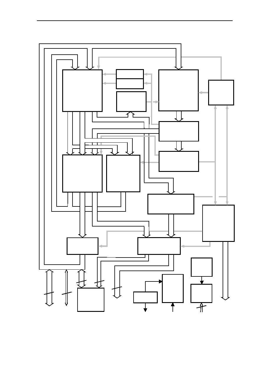
0.2 Block Diagram
Figure 0.1: Block Diagram
DSP
Execution
Unit
Hardware-
Multiplier
Store Data
Pipeline
Instruction Prefetch
Control Unit
DataBus Parity
ALU
Barrel shifter
Z
W
A
X
Y
I
Memory Address
Pipeline
Address
Bus
Control
Bus
Bus Interface
Control Unit
Bus Pipeline
Control
Instruction
Cache
Control
Instruction
Cache
Load
Decode
Instruction
Decode
32
26
8 kByte
RAM
12
X
Y
PC
Instruction
Execution
Control Unit
Interrupt
control
Internal
Timer
32
Watchdog
Power
Down+
Reset
Control
4
(16)
(22)
4
(2)
Register Set
64 Local
26 Global
X-Decode
Y-Decode
X Y
0-8 CHAPTER 0
0.3 Pin Configuration
0.3.1 GMS30C2232, 160-Pin MQFP-Package - View from Top Side
2
1
3
4
5
6
7
8
9
10
11
12
13
14
15
16
17
18
19
20
21
22
23
24
25
108
107
106
105
104
103
102
101
100
99
98
96
95
94
93
92
91
90
89
88
87
86
85
84
121
122
123
124
125
126
127
128
129
130
131
132
133
97
48
47
46
45
44
43
42
41
71
70
69
68
67
66
65
64
63
62
49
50
A24
A23
GND
VCC
A22
A8
A7
VCC
A6
A5
A4
GND
WE0#/BE0#
WE1# /BE1#
VCC
CAS0#
A14
GND
VCC
ACT
A13
GND
WE#
GND
VCC
VCC
D23
D22
GND
D5
D4
D3
VCC
D2
D1
D0
VCC
GND
D21
D20
D19
DP2
DP3
VCC
GND
RESET#
GRANT#
VCC
GND
VCC
VCC
GND
IO3
IO
WR#
CS3#
CS2#
CS1#
GND
RAS#
A19
VCC
A20
A21
GND
D31
D30
D29
A9
A10
A11
A12
VCC
D28
D27
D26
GND
W
E2#
/BE2#
IORD#
OE#
VCC
CAS3#
CAS2#
CAS1#
GND
XTAL1/CLKIN
XTAL2
IO2
VCC
D16
D17
D18
A3
A2
A1
A0
GND
DP1
DP0
83
82
81
BOOT
W
CLKOUT
IO1
GND
RQST
INT4
INT3
/
W
AI
T
INT2
INT1
GND
VCC
61
60
59
58
57
56
55
54
53
52
51
VCC
GND
D9
GND
D8
D7
VCC
GND
D6
D24
26
27
28
29
30
31
32
33
34
35
36
GND
D25
D15
D14
VCC
D13
D12
D11
D10
GND
VCC
134
135
136
137
138
139
140
141
142
143
144
VCC
GND
BOOTB
A18
A17
GND
VCC
A16
A15
A25
GND
72
GND
VCC
W
E3#
/BE3#
NC
NC
NC
NC
109
110
111
112
113
114
115
116
117
118
119
120
73
74
75
76
77
78
79
80
N C
N C
N C
N C
37
38
39
40
NC
NC
NC
NC
145
146
147
148
149
150
151
152
153
154
155
156
157
158
159
160
N C
N C
N C
N C
GMS30C2232
Figure 0.2: GMS30C2232, 160-Pin MQFP-Package

Overview 0-9
0.3.2 Pin Cross Reference by Pin Name
Signal Location Signal Location Signal Location Signal Location
A0................... 97 D3 .....................59 GND ................. 50 NC................... 118
A1................... 98 D4 .....................58 GND ................. 56 NC................... 123
A2................... 99 D5 .....................57 GND ................. 65 NC................... 124
A3................. 100 D6 .....................51 GND ................. 68 NC................... 157
A4................. 137 D7 .....................48 GND ................. 73 NC................... 158
A5................. 138 D8 .....................47 GND ................. 79 OE #................ 113
A6................. 139 D9 .....................45 GND ................. 82 RAS# ................ 11
A7................. 141 D10 ...................36 GND ................. 90 RESET#............ 74
A8................. 142 D11....................35 GND ................. 96 RQST................ 89
A9................... 20 D12 ...................34 GND ............... 108 VCC .................... 1
A10................. 21 D13 ...................33 GND ................119 VCC .................. 13
A11 ................. 22 D14 ...................31 GND ............... 122 VCC .................. 24
A12................. 23 D15 ...................30 GND ............... 126 VCC .................. 32
A13............... 127 D16 .................103 GND ............... 130 VCC .................. 40
A14............... 131 D17 .................102 GND ............... 136 VCC .................. 41
A15............... 150 D18 .................101 GND ............... 145 VCC .................. 49
A16............... 151 D19 ...................69 GND ............... 148 VCC .................. 53
A17............... 154 D20 ...................67 GND ............... 153 VCC .................. 60
A18............... 155 D21 ...................66 GND ............... 159 VCC .................. 64
A19................. 12 D22 ...................55 GRANT#........... 75 VCC .................. 72
A20................. 14 D23 ...................54 INT1.................. 85 VCC .................. 76
A21................. 15 D24 ...................52 INT2.................. 86 VCC .................. 80
A22............... 143 D25 ...................29 INT3/WAIT........ 87 VCC .................. 81
A23............... 146 D26 ...................27 INT4.................. 88 VCC ................ 104
A24............... 147 D27 ...................26 IO1.................... 91 VCC ................ 112
A25............... 149 D28 ...................25 IO2.................. 105 VCC ................ 120
ACT .............. 128 D29 ...................19 IO3...................... 5 VCC ................ 121
BOOTB......... 156 D30 ...................18 IORD# .............114 VCC ................ 129
BOOTW.......... 93 D31 ...................17 IOWR#................ 6 VCC ................ 133
CAS0#.......... 132 DP0 ...................94 NC ...................... 3 VCC ................ 140
CAS1#.......... 109 DP1 ...................95 NC ...................... 4 VCC ................ 144
CAS2#.......... 110 DP2 ...................70 NC .................... 37 VCC ................ 152
CSS3#...........111 DP3 ...................71 NC .................... 38 VCC ................ 160
CLKOUT
......... 92 GND ....................2 NC .................... 43 WE# ................ 125
CS1# ................ 9 GND ..................10 NC .................... 44 WE0#/BE0# .... 135
CS2#
................. 8 GND ..................16 NC .................... 77 WE1#/BE1# .... 134
CS3# ................ 7 GND ..................28 NC .................... 78 WE2#/BE2# .... 115
D0................... 63 GND ..................39 NC .................... 83 WE3#/BE3# .... 116
D1................... 62 GND ..................42 NC .................... 84 XTAL1/CLKIN . 107
D2................... 61 GND ..................46 NC ...................117 XTAL2 ............. 106

0-10 CHAPTER 0
0.3.3 Pin Function
Type
Name
State
Use
Power
VCC
I
Power. Connected to the power supply. It can be 3.3V power
supply.
GND
I
Ground. Connected to the system ground. All GND pins must
be connected to the system ground.
Clock
XTAL1
I
Input for Quartz Clock. When the clock is generated by
external clock generator, XTAL1 is used as clock input.
XTAL2
O
Output for Quartz Clock.
CLKOUT
O
Clock Signal Output. It can be used to supply a clock signal to
peripheral devices.
Address Bus
A25..A0
O/Z Address Bus. With the GMS30C2232, only A22..A0 are
connected to the address bus pins
Data Bus
D31..D0
I/O Data Bus. 32-bit bidirectional data bus
DP0..DP3
I/O Data Parity Signal. Bidirectional parity signals
Bus Control
RAS#
O/Z Row Address Strobe. RAS# is activated when the processor
accesses a DRAM or refresh cycle. When a SRAM is placed in
MEM0, RAS# is used as the chip select signal
CAS0#..CAS3# O/Z Column Address Strobe. They are only used by a DRAM for
column access cylices and for "CAS before RAS" refresh.
WE#
O/Z Write Enable. Active low indicates a write access, active high
indicates a read access.
CS1#..CS3#
O/Z Chip Select. Active low of CS1#..CS3# indicates chip select
for the memory areas MEM1..MEM3.
WE0#..WE3#
O/Z SRAM Write Enable. Active low indicates write enable for the
corresponding byte.
OE#
O/Z Output Enable for SRAMs and EPROMs.
IORD#
O/Z I/O Read Strobe, optionally I/O Data Strobe. The use of
IORD# is specified in the I/O address bit 10.
IOWR#
O/Z I/O Write Strobe.
Bus Control
RQST
O
RQST signals the request for a memory or I/O access
GRANT#
I
Bus Grant. GRANT# is signaled low by an bus arbiter to grant
access to the bus for memory and I/O cycles
ACT
O
Active as bus master. ACT is signaled high when GRANT# is
low and it is kept high during a current bus access
Interrupt
INT1..INT4
I
Interrupt Request A signal of INT1..INT4 interrupt request
pins causes an interrupt exception when interrupt lock flag L is
clear and the corresponding INTxMask bit in FCR is not set.
I/O Port
IO1..IO3
I/O General Input-Output Port. IO1..IO3 can be individually
configured via IOxDirection bits in the FCR as either input or
output pins (port).
System Control
RESET#
I
Reset Processor. RESET# low resets the processor to the initial
state and halts all activity. RESET# must be low for at least
two cycles

ARCHITECTURE 1-1
1. Architecture
1.1 Introduction
1.1.1 RISC Architecture
In the early days of computer history, most computer families started with an instruction
set which was rather simple. The main reason for being simple then was the high cost for
hardware. The hardware cost has dropped and the software cost has gone up steadily in the
past three decades.
The net result is that more and more functions have been built into the hardware, making
the instruction set very large and very complex. The growth of instruction sets was also
encouraged by the popularity of microprogrammed control in the 1960s and 1970s. Even
user-defined instruction sets were implemented using microcodes in some processors for
special-purpose applications.
The evolution of computer architectures has been dominated by families of increasingly
complex processors. Under market pressures to preserve existing software, Complex
Instruction Set Computer (CISC) architectures evolved by the gradual addition of
microcode and increasingly elaborate operations. The intent was to supply more support
for high-level languages and operating systems, as semiconductor advances made it
possible to fabricate more complex integrated circuits. It seemed self-evident that
architectures should become more complex as these technological advances made it
possible to hold more complexity on VLSI devices.
In recent years, however, Reduced Instruction Set Computer (RISC) architectures have
implemented a much more sophisticated handling of the complex interaction between
hardware, firmware and software. RISC concepts emerged from statistical analysis of how
software actually uses the resources of a processor. Dynamic measurement of system
kernels and object modules generated by optimizing compilers show an overwhelming
predominance of the simplest instruction, even in the code for CISC machine. Complex
instructions are often ignored because a single way of performing a complex operation
needs of high-level language and system environments. RISC designs eliminate the
microcoded routines and turn the low-level control of the machine over to software.
This approach is not new. But its application is more universal in recent years thanks to the
prevalence of high-level languages, the development of compilers that can optimize at the
microcode level, and dramatic advances in semiconductor memory and packaging. It is
now feasible to replace machine microcode ROM with faster RAM, organized as an
instruction cache. Machine control then resides in the instruction cache and is, in fact,
customized on the fly. The instruction stream generated by system- and compiler-generated
code provides a precise fit between the requirements of high-level software and the
capabilities of the hardware. So compilers are playing a vital role in RISC performance.
The advantage of RISC architecture is described as follows:
·
Simplicity made VLSI implementation possible and thus higher clock rates.
·
Hardwired control and separated data and program caches lower the average CPI
(Cycles per Instruction) significantly.

1-2 CHAPTER 1
·
Dynamic instruction count in a RISC program only increased slightly (less than 2)
inordinary program.
·
Recently, the MIPS (Million Instructions per Second) rate of a typical RISC
microprocessor increased with a factor of 5/(2*0.1) = 25 times from that of a typical
CISC microprocessor.
·
The clock rate increased from 10 MHz on a CISC processor to 50 MHz on a CMOS/
RISC microprocessor.
·
The instruction count in a typical RISC program increased less than 2 times form that of
a typical CISC program.
·
The average CPI for a RISC microprocessor decreased to 1.2 (instead of 12 as in a
typical CISC processor).
1.1.2 Techniques to reduce CPI (Cycles per Instruction)
If the work each instruction performs is simple and straightforward, the time required to
execute each instruction can be shortened and the number of cycles reduced. The goal of
RISC designs has been to achieve an execution rate of one instruction per machine cycle
(multiple-instruction-issue designs now seek to increase this rate to more than one
instruction per cycle). Techniques that help achieve this goal include:
·
Instruction pipelines
·
Load and store (load/store) architecture
·
Delayed load instructions
·
Delayed branch instructions
(1) Instruction Pipelines
One way to reduce the number of cycles required to execute an instruction is to overlap the
execution of multiple instructions. Instruction pipelines divide the execution of each
instruction into several discrete portions and then execute multiple instructions
simultaneously. The instruction pipeline technique can be likened to an assembled line -
the instruction progresses from one specialized stage to the next until it is complete (or
issued) - just as an automobile moves along an assembly line. (This is contrast to the
nonpipeline, microcode approach, where all the work is done by one general unit and is
less capable at each individual task.) For example, the execution of an instruction might be
subdivided into four portions, or clock cycles, as shown in Figure 1.1:
Fetch
Instruction
(F)
ALU
Operation
(A)
Access
Memory
(M)
Write
Results
(W)
Cycle
#1
Cycle
#2
Cycle
#3
Cycle
#1
Figure 1.1: Functional Division of a Hypothetical Pipeline
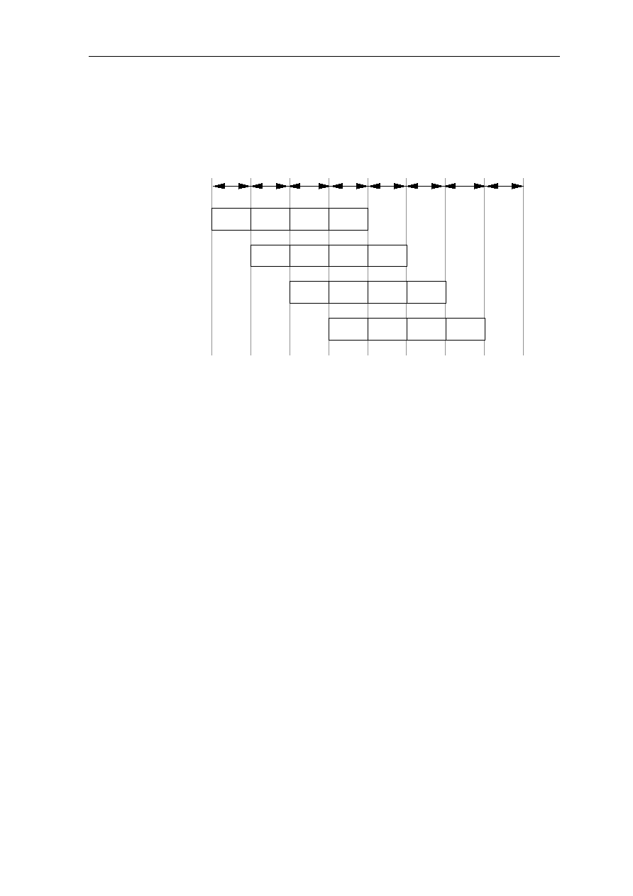
ARCHITECTURE 1-3
An Instruction pipeline can potentially reduce the number of cycles/instructions by a factor
equal to the depth of the pipeline (the depth of the pipeline = the number of resource). For
example, in Figure 3.2 each instruction still requires a total of four clock cycles to execute.
However, if the four-level instruction-pipeline is used, a new instruction can be initiated at
each clock cycle and the effective execution rate is one cycle per instruction.
F
A
M
W
# 1
# 2
# 3
# 4
F
A
M
W
F
A
M
W
F
A
M
W
C l o c k C y c les
Instruction
Figure 1.2: Multiple Instructions in a Hypothetical Pipeline
(2) Load/Store Architecture
The discussion of the instruction pipeline illustrates how each instruction can be
subdivided into several discrete parts that permit the processor to execute multiple
instructions in parallel. For this technique to work efficiently, the time required to execute
each instruction subpart should be approximately equal. If one part requires an excessive
length of time, there is an unpleasant choice: either halting the pipeline (inserting wait or
idle cycles), or making all cycles longer to accommodate this lengthier portion of the
instruction.
Instructions that perform operations on operands in memory tend to increase either the
cycle time or the number of cycles/instruction. Such instruction require additional time for
execution to calculate the addresses of the operands, read the required operands from
memory, calculate the result, and store the results of the operation back to memory. To
eliminate the negative impact of such instruction, RISC designs implement a load and store
(load/store) architecture in which the processor has many register, all operations are
performed on operands held in processor registers, and main memory is accessed only by
load and store instructions.
This approach produces several benefits
·
Reducing the number of memory accesses eases memory bandwidth requirements
·
Limiting all operations to registers helps simplicity the instruction set
·
Eliminating memory operations makes it easier for compilers to optimize register
allocation - this further reduces memory accesses and also reduces the instructions/task
factor
1-4 CHAPTER 1
All of these factors help RISC design approach their goal of executing one
cycle/instruction. However, two classes of instructions hinder achievement of this goal -
load instructions and branch instructions. The following sections discuss how RISC
designs overcome obstacles raised by these classes of instructions.
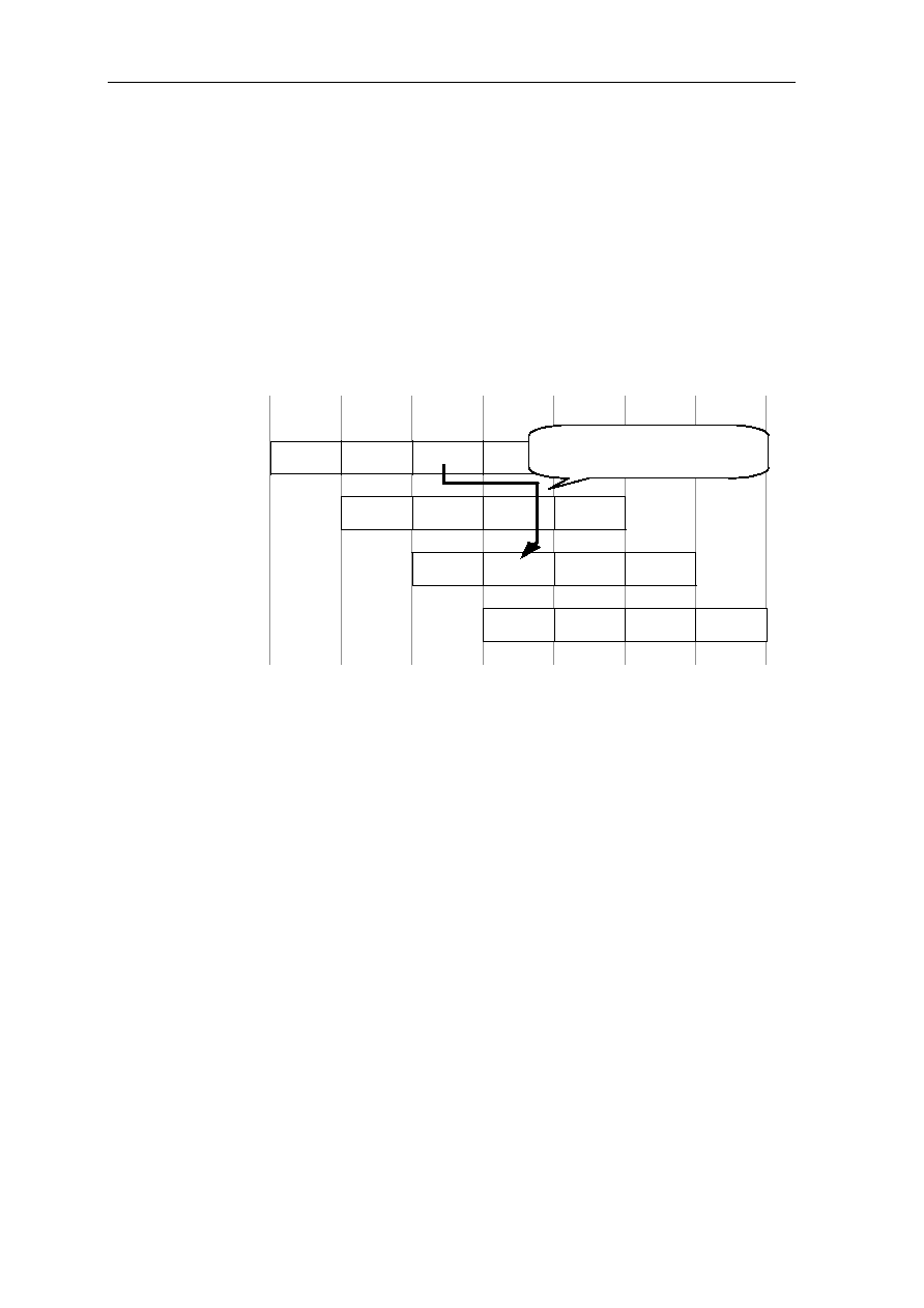
(3) Delayed Load Instructions
Load instruction read operands from memory into processor register for subsequent
operation by other instructions. Because memory typically operates at much slower speeds
than processor clock rates, the loaded operand is not immediately available to subsequent
instructions in an instruction pipeline. The data dependency is illustrated in Figure 1.3.
F
A
M
W
1
2
3
4
F
A
M
W
F
A
M
W
F
A
M
W
D a t a f r o m L o a d
a v a i l a b l e a s o p e r a t i o n
L o a d
I n s t r u c t i o n
Figure 1.3: Data Dependency Resulting From a Load Instruction
In this illustration, the operand loaded by instruction 1 is not available for use in the A
cycle (ALU, or Arithmetic/Logic Unit operation) of instruction 2. One way to handle this
dependency is to delay the pipeline by inserting additional clock cycles into the execution
of instruction 2 until the loaded data becomes available. This approach obviously
introduces delays that would increase the cycles/instructions factor.
In many RISC design the technique used to handle this data dependency is to recognize
and make visible to compilers the fact that all load instructions have an inherent latency or
load delay. Figure 3.3 illustrates a load delay or latency of one instruction. The instruction
that immediately follows the load is in the load delay slot. If the instruction in this slot does
not require the data from the load, and then no pipeline delay is required.
If this load delay is made visible to software, a compiler can arrange instructions to ensure
that there is no data dependency a load instruction and the instruction in the load delay slot.
The simplest way of ensuring that there is no data dependency is to insert a No Operation
(NOP) instruction to fill the slot, as follow:
Load R1, A
Load R2, B
NOP <= This instruction fills the delay slot
ADD R3, R1, R2
Although filling the delay slot with NOP instructions eliminates the need for hardware-
controlled pipeline stalls in this case, it still is not a very efficient use of the pipeline stream
ARCHITECTURE 1-5
since these additional NOP instructions increase code size and perform no useful work. (In
practice, however, this technique need not have much negative impact on performance.)
A more effective solution to handling the data dependency is to fill the load delay slot with
a useful instruction. Good optimizing compilers can usually accomplish this, especially if
the load delay is only one instruction. Below example program illustrates how a compiler
might rearrange instruction to handle a potential data dependency.
# Consider the code for C := A+B; F := D
Load R1, A
Load R2, B
Add R2, R1, R2 <= This instruction stalls because R2 data is not available
Load R4, D
..... ....
# An alternative code sequence (where delay length = 1)
Load R1, A
Load R2, B
Load R4, D
Add R3, R1, R2 <= No stall since R2 data is available
(4) Delayed Branch Instructions
Branch instructions usually delay the instruction pipeline because the processor must
calculate the effective destination of the branch and fetch that instruction. When a cache
access requires an entire cycle, and the fetched branch instruction specifies the target
address, it is impossible to perform this fetch (of the destination instruction) without
delaying the pipeline for at least one pipe stage (one cycle). Conditional branches can
cause further delays because they require the calculation of a condition, as well as the
target address.
Instead of stalling the instruction pipeline to wait for the instruction at the target address,
RISC designs typically use an approach similar to that used with Load instruction: Branch
instructions are delayed and do not take effect until after one or more instructions
immediately following the Branch instruction have been executed. The instruction or
instructions immediately following the Branch instruction (delay instruction) have been
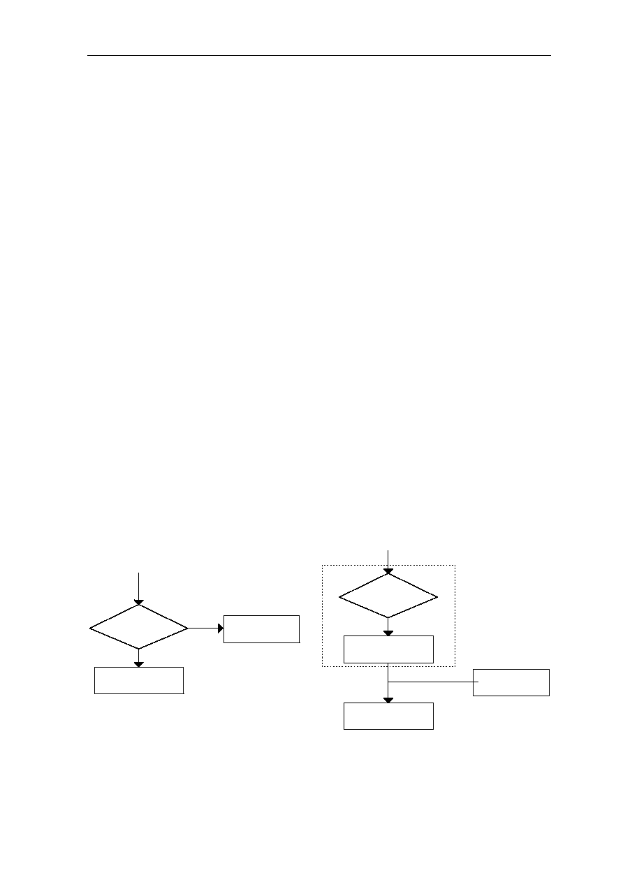
executed. Branch and delayed branch instruction are illustrated in Figure 1.4
Next Instruction
Branch Target
Condition ?
YES
NO
Next Instruction
Branch Target
Condition ?
NO
Delay Instruction
YES
Delayed Branch
Branch Instruction
Delayed Branch Instruction
Figure 1.4: Block Diagram of Branch/Delayed Branch Instruction

1-6 CHAPTER 1
1.1.3 The pipeline structure of GMS30C2232
GMS30C2232 has a two-stage pipeline structure and each stage is composed of two phases
(TM and TV). The basic structure of GMS30C2232 pipeline is two-stage pipeline, but
actually it is lengthened by the need of some instruction. As a example, standard ALU
instruction uses 5 phases (2 stage pipeline (4 phases) + additional 1 phase). This additional
phase doesn't use the datapath which is used next instruction, so nex t instruction execution
need not wait until previous ALU instruction is ended. DSP instruction takes over 2 stage
pipeline for execution, and requires same resource in the datapath which is required to next
DSP instruction. So next DSP instruction is delayed.
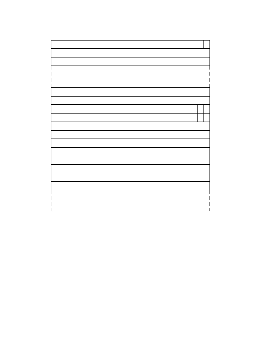
The pipeline structure of GMS30C2232 and the action of datapath is described in Table 1.1.
Stage
Phase
Datapath Action
Fetch/Decode TM (Low) 1. The instruction is read from the instruction cache
according to the address of instruction.
TV (High) 2. The control signal of Rd (destination operand) and Rs
(source operand) is activated according to the instruction
that was loaded in TM phase
2.1 The control signal of IR (immediate register
(operand)) and IL (instruction length) is activated.
2.2 The address of next instruction is calculated and saved
in PC
Execute/Write TM (Low) 1. The next instruction is read from the instruction cache.
1.1 The address of Rs and Rs are determined.
1.2 The immediate operand is determined.
1.3 The operand is read from register stack using the
address of Rs and Rd.
1.4 The operand XR, YR and QR are controlled.
TV (High) 2. The input data of ALU is attained.
2.1 The control of ALU datapath is made and instruction
is executed in ALU.
2.2 The result of ALU operation is saved in the register
file.
Additional
Insertion
Next TM Additional ALU operation is continued and its result is
saved in the register file.
Table 1.1: The pipeline structure of GMS30C2232 and the action of datapath.

ARCHITECTURE 1-7
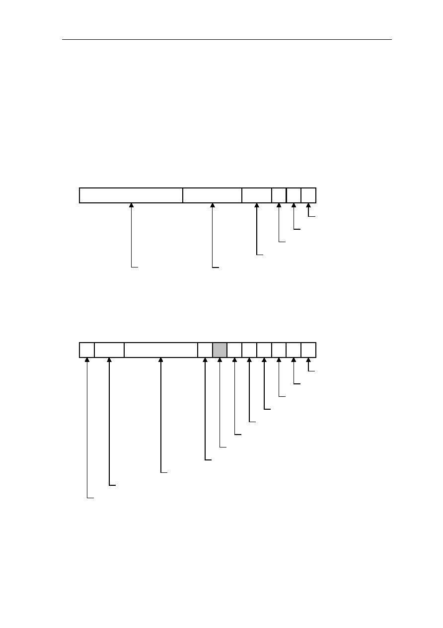
1.2 Global Register Set
The architecture provides
32
global registers of 32bit each. These are:
G0 Program Counter PC
G1 Status Register SR
G2 Floating-point Exception Register FER
G3..G15 General purpose registers
G16..G17 Reserved
G18 Stack Pointer SP
G19 Upper stack Bound UB
G20 Bus Control Register BCR (see section 6. Bus Interface)
G21 Timer Prescaler Register TPR (see
section 5. Timer and CPU Clock
Modes
)
G22 Timer Compare Register TCR (see
section 5. Timer and CPU Clock
Modes
)
G23 Timer Register TR (see
section 5. Timer and CPU Clock Modes
)
G24 Watchdog Compare Register WCR (see
section 6. Bus Interface
)
G25 Input Status Register ISR (see
section 6. Bus Interface
)
G26 Function Control Register FCR (see
section 6. Bus Interface
)
G27 Memory Control Register MCR (see
section 6. Bus Interface
)
G28..G31 Reserved
Registers G0..G15 can be addressed directly by the register code (0..15) of an instruction.
Registers G18..G27 can be addressed only by a MOV or MOVI instruction with the high
global flag H set to 1.
(Example)
MOVI G2, 0x20 ; G2 := 0x20 (set H flag)
MOV G3, G19 ; G3 := G19 (G19 (UB) is copied to G3)
1-8 CHAPTER 1
G0
0
31
0
G1
G2
G3
G15
G16
G17
G18
G19
G20
G21
G22
G23
G24
G25
G26
G27
Program Counter PC
Status Register SR
Floating-Point Exception Register FER
Reserved
Reserved
General Purpose Registers G3..G15
Stack Pointer SP
Upper Stack Bound UB
Bus Control Register BCR
Timer Prescaler Register TPR
Timer Compare Register TCR
Timer Register TR
Watchdog Compare Register WCR
Input Status Register ISR
Function Control Register FCR
Memory Control Register MCR
G28..G31 Reserved
0
0
0
0
G28
G31
Figure 1.5: Global Register Set
1.2.1 Program Counter PC, G0
G0 is the program counter PC. It is updated to the address of the next instruction through
instruction execution. Besides this implicit updating, the PC can also be addressed like a
regular source or destination register. When the PC is referenced as an operand, the
supplied value is the address of the first byte after the instruction which references it (the
address of next instruction), except when referenced by a delay instruction with a
preceding delayed branch taken. At delay branch instruction, when the branch condition is
met, place the branch address PC + rel (relative to the address of the first byte after the
Delayed Branch Instruction) in the PC (see
section 1.26. Delayed Branch Instructions
).
Placing a result in the PC has the effect of a branch taken. When branch is taken, the target
address of branch is placed in PC.
Bit zero of the PC is always zero, regardless of any value placed in the PC.
ARCHITECTURE 1-9
1.2.2 Status Register SR, G1
G1 is the status register SR. Its content is updated by instruction execution. Besides this
implicit updating, the SR can also be addressed like a regular register (when H flag is set).
When addressed as source or destination operand, all 32 bits are used as an operand.
However, only bits 15..0 of a result can be placed in bits 15..0 of the SR, bits 31..16 of the
result are discarded and bits 31..16 of the SR remain unchanged. When SR addressed as
source operand, it represents 0x0 value. The full content of the SR is replaced only by the
Return Instruction. A result placed in the SR overrules any setting or clearing of the
condition flags as a result of an instruction.
Frame Pointer
Frame Length
28
29
FL
S
P
T
Trace-Mode Flag
Trace Pending Flag
Supervisor State Flag
Instruction-Length Code
31 30
27 26 25 24 23 22 21 20 19 18 17 16
ILC
FP
Figure 1.6: Status Register SR (bits 31..16)
Floating-Point Rounding Mode
Floating-Point Trap Enable
Interrupt-Mode Flag
High Global Flag
Cache-Mode Flag
12
13
FTE
V
N
Z
C
Carry Flag
Zero Flag
Negative Flag
Overflow Flag
15 14
11 10
9
8
7
6
5
4
3
2
1
0
M
H
FRM
L
I
Reserved
Interrupt-Lock Flag
Figure 1.7: Status Register SR (bits 15..0)

1-10 CHAPTER 1
The status register SR contains the following status information:
C Carry Flag. Bit zero is the carry condition flag C. In general, when set it
indicates that the unsigned integer range is exceeded (overflow). At add
operations, it indicates a carry out of bit 31 of the result. At subtract operations,
it indicates a borrow (inverse carry) into bit 31 of the result.
Z Zero Flag. Bit one is the zero condition flag Z. When set, it indicates that all 32
or 64 result bits are equal to zero regardless of any carry, borrow or overflow.
N Negative Flag. Bit two is the negative condition flag N. On compare
instructions, it indicates the arithmetic correct (true) sign of the result
regardless of an overflow. On all other instructions, it is derived from result bit
31, which is the true sign bit when no overflow occurs. In the case of overflow,
result bit 31 and N reflect the inverted sign bit.
V Overflow Flag. Bit three is the overflow condition flag V. In general, when set
it indicates a signed overflow. At the Move instructions, it indicates a floating-
point NaN (Not a Number).
M Cache-Mode Flag. Bit four is the cache-mode flag M. Besides being set or
cleared under program control, it is also automatically cleared by a Frame
instruction and by any branch taken except a delayed branch. See
section
1.8. Instruction Cache
for details.
H
High Global Flag. Bit five is the high global flag H. When H is set, denoting
G0..G15 addresses G16..G31 instead. Thus, the registers G18..G27 may be
addressed by denoting G2..G11 respectively.
The H flag is effective only in the first cycle of the next instruction after it was
set; then it is cleared automatically.
Only the MOV or MOVI instruction issued as the next instructions must be
used to copy the content of a local register or an immediate value to one of the
high global registers. The MOV instruction may be used to copy the content of
a high global register (except the BCR, TPR, FCR and MCR register, which
are write-only) to a local register. With all other instructions, the result may be
invalid.
If one of the high global registers is addressed as the destination register in user
state (S = 0), the condition flags are undefined, the destination register remains
unchanged and a trap to Privilege Error occurs.
Reserved Bit six is reserved for future use. It must always be zero.
I Interrupt-Mode Flag. Bit seven is the interrupt-mode flag I. It is set
automatically on interrupt entry and reset to its old value by a Return
instruction. The I flag is used by the operating system; it must be never
changed by any user program.
FTE Floating-Point Trap Enable Flag. Bits 12..8 are the floating-point trap enable
flags They determine the Exception type and Trap execution flow(see
section
3.33.2. Floating-Point Instructions
).
FRM Floating-Point Rounding Mode. Bits 14..13 are the floating-point rounding
modes (see
section 3.33.2. Floating-Point Instructions
).

ARCHITECTURE 1-11
L Interrupt-Lock Flag. Bit 15 is the interrupt-lock flag L. When the L flag is one,
all Interrupt, Parity Error and Extended Overflow exceptions are inhibited
regardless of individual mode bits. The state of the L flag is effective
immediately after any instruction which changed it. The L flag is set to one by
any exception.
The L flag can be cleared or kept set in any or on return to any privilege state
(user or supervisor). Changing the L flag from zero to one is privileged to
supervisor or return from supervisor to supervisor state. A trap to Privilege
Error occurs if the L flag is set under program control from zero to one in user
or on return to user state.
The following status information cannot be changed by addressing the SR:
T Trace-Mode Flag. Bit 16 is the trace-mode flag T. When both the T flag and
the trace pending flag P are one, a trace exception occurs after every instruction
except after a Delayed Branch instruction. The T flag is cleared by any
exception.
Note: The T flag can only be changed in the saved return SR and is then
effective after execution of a Return instruction.
P Trace Pending Flag. Bit 17 is the trace pending flag P. It is automatically set to
one by all instructions except by the Return instruction, which restores the P
flag from bit 17 of the saved return SR.
Since for a Trace exception both the P and the T flag must be one, the P flag
determines whether a trace exception occurs (P = 1) or does not occur (P = 0)
immediately after a Return instruction that restored the T flag to one.
When an instruction is ended, the T and P flag set to one. Therefore trace
exception is occurred. After trace exception trap is ended the process returns to
main program, and if T and P flag is set to one, trace exception occurs again.
To avoid tracing the same instruction in an endless loop, the P flag is cleared at
return instruction in trace exception trap routine.
Note: The P flag can only be changed in the saved SR. No program except the
trace exception handler should affect the saved P flag. The trace exception
handler must clear the saved P flag to prevent a trace exception on return, in
order to avoid tracing the same instruction in an endless loop.
S Supervisor State Flag. Bit 18 is the supervisor state flag S (see section
1.4. Privilege States). The S flag determine whether user state (S=0) or
supervisor state (S=1). It is set to one by any exception.
ILC Instruction-Length Code. Bits 20 and 19 represent the instruction-length code
ILC. It is updated by instruction execution. The ILC holds (in general) the
length of the last instruction: ILC values of one, two or three represent an
instruction length of one, two or three halfwords respectively. After a branch
taken, the ILC is invalid. The Return instruction clears the ILC.
Note: Since a Return instruction following an exception clears the ILC, a
program must not rely on the current value of the ILC.
FL Frame Length. Bits 24..21 represent the frame length FL. The FL holds the
number of usable local registers (maximum 16) assigned to the current stack
frame. FL = 0 is always interpreted as FL = 16.
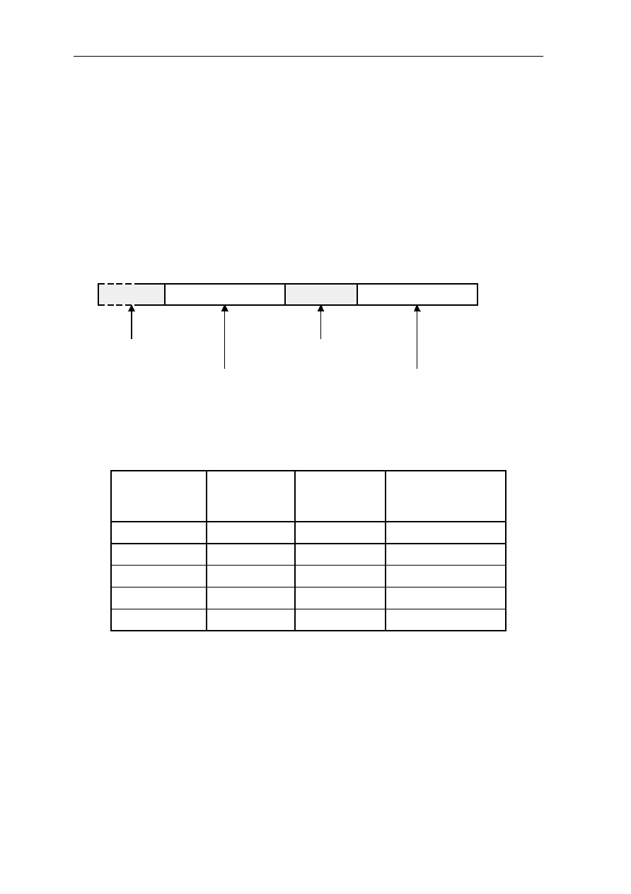
1-12 CHAPTER 1
FP Frame Pointer. Bits 31..25 represent the frame pointer FP. The least significant
six bits of the FP point to the beginning of the current stack frame in the local
register set, that is, they point to L0.
The FP contains bit 8..2 of the address at which the content of L0 would be
stored if pushed onto the memory part of the stack.
1.2.3 Floating-Point Exception Register FER, G2
G2 is the floating-point exception register. All bits must be cleared to zero after Reset.
Only bits 12..8 and 4..0 may be changed by a user program, all other bits must remain
unchanged.
Reserved
Floating-Point Actual Exceptions
Reserved for Operating System
Floating-Point Accrued Exceptions
12
13
11
10
9
8
7
6
5
4
3
2
1
0
31
Figure 1.8: Floating-Point Exception Register
The floating-point trap enable flags FTE and the exception flags are assigned as:
floating-point
trap enable
FTE
Accrued
exceptions
Actual
exceptions
exception type
SR(12)
G2(4)
G2(12)
Invalid Operation
SR(11)
G2(3)
G2(11)
Division by Zero
SR(10)
G2(2)
G2(10)
Overflow
SR(9)
G2(1)
G2(9)
Underflow
SR(8)
G2(0)
G2(8)
Inexact
The reserved bits G2(31..13) and G2(7..5) must be zero.
A floating-point instruction, except a Floating-point Compare, can raise any of the
exceptions Invalid Operation, Division by Zero, Overflow, Underflow or Inexact. FCMP
and FCMPD can raise only the Invalid Operation exception (at unordered). FCMPU and
FCMPUD cannot raise any exception.

ARCHITECTURE 1-13
At an exception, the following additional action is performed:
·
Any corresponding accrued-exception flag whose corresponding trap-enable flag is
zero (not enabled) is set to one; all other accrued-exception flags remain unchanged.
·
If a corresponding trap-enable flag is one (enabled), any corresponding actual-ex-
ception flag is set to one; all other actual-exception flags are cleared. The destination
remains unchanged.
In the present software version, the software emulation routine must branch to the
corresponding user-supplied exception trap handler. The (modified) result, the source
operand, the stack address of the destination operand and the address of the floating-point
instruction are passed to the trap handler. In the future hardware version, a trap to Range
Error will occur; the Range Error handler will then initiate re-execution of the floating-
point instruction by branching to the entry of the corresponding software emulation routine,
which will then act as described before.
The only exceptions that can coincide are Inexact with Overflow and Inexact with
Underflow. An Overflow or Underflow trap, if enabled, takes precedence over an Inexact
trap; the Inexact accrued-exception flag G2(0) must then be set as well.
1.2.4 Stack Pointer SP, G18
G18 is the stack pointer SP. The SP contains the top address + 4 of the memory part of the
stack, that is the address of the first free memory location in which the first local register
would be saved by a push operation (see section 3.29. Frame Instruction for details). Stack
growth is from low to high address.
Bits one and zero of the SP must always be cleared to zero. The SP can be addressed only
via the high global flag H being set. Copying an operand to the SP is a privileged operation.
Note: Stack Pointer SP contains the top address + 4 of the memory part of the stack
(memory part stack), and Frame Pointer FP points to the beginning of the current stack
frame in the local register set (register part stack).
1.2.5 Stack Pointer SP, G18
G19 is the upper stack bound UB. The UB contains the address beyond the highest legal
memory stack location. It is used by the Frame instruction to inhibit stack overflow.
Bits one and zero of the UB must always be cleared to zero. The UB can be addressed only
via the high global flag H being set. Copying an operand to the UB is a privileged
operation.
1.2.6 Bus Control Register BCR, G20
G20 is the write-only bus control register BCR. Its content defines the options possible for
bus cycle, parity and refresh control. The BCR defines the parameters (bus timing, refresh
control, page fault and parity error disable) for accessing external memory located in
address spaces MEM0..MEM3. The BCR can be addressed only via the high global flag H
being set. Copying an operand to the BCR is a privileged operation. The BCR register is
described in detail in the bus interface description in
section 6
.

1-14 CHAPTER 1
1.2.7 Timer Prescaler Register TPR, G21
G21 is the write-only timer prescaler register TPR. It adapts the timer clock to different
processor clock frequencies. The TCR can be addressed only via the high global flag H
being set. Copying an operand to the TPR is a privileged operation. The TPR is described
in the timer description in
section 5
.
1.2.8 Timer Compare Register TCR, G22
G22 is the timer compare register TCR. Its content is compared continuously with the
content of the timer register TR. The TCR can be addressed only via the high global flag H
being set. Copying an operand to the TCR is a privileged operation. The TCR is described
in the timer description in
section 5
.
1.2.9 Timer Register TR, G23
G23 is the timer register TR. Its content is incremented by one on each time unit. The TR
can be addressed only via the high global flag H being set. Copying an operand to the TR
is a privileged operation. The TR is described in the timer description in
section 5
.
1.2.10 Watchdog Compare Register WCR, G24
G24 is the watchdog compare register WCR. The WCR can be addressed only via the high
global flag H being set. The WCR is used by the IO3 control mode (Watchdog Mode
FCR(13) = 1, FCR(12) = 0). Copying an operand to the WCR is a privileged operation.
The WCR is described in the bus interface description in
section 6
.
1.2.11 Input Status Register ISR, G25
G25 is the read-only input status register ISR. The ISR reflects the input levels at the pins
IO1..IO3 as well as the input levels at the four interrupt pins INT1..INT4 and contains the
EvenFlag and the EqualFlag. The ISR can be addressed only via the high global flag H
being set. The ISR is described in the bus interface description in
section 6
.
1.2.12 Function Control Register FCR, G26
G26 is the write-only function control register FCR. The FCR controls the polarity and
function of the I/O pins IO1..IO3 and the interrupt pins INT1..INT4, the timer interrupt
mask and priority, the bus lock and the Extended Overflow exception. The FCR can be
addressed only via the high global flag H being set. Copying an operand to the FCR is a
privileged operation. The FCR is described in the bus interface description in
section 6
.
1.2.13 Memory Control Register MCR, G27
G27 is the write-only memory control register MCR. The MCR controls additional
parameters for the external memory, the internal memory refresh rate, the mapping of the
entry table and the processor power management. The MCR can be addressed only via the
high global flag H being set. Copying an operand to the MCR is a privileged operation.
The MCR is described in the bus interface description in
section 6
.
ARCHITECTURE 1-15
1.3 Local Register Set
The architecture provides a set of 64 local registers of 32 bits each. The local registers
0..63 represent the register part of the stack, containing the most recent stack frame(s).
0
Local Register L0
Local Register L15
31
0
L0
L15
63
Figure 1.9: Local Register Set 0..63
The local registers can be addressed by the register code (0..15) of an instruction as
L0..L15 only relative to the frame pointer FP; they can also be addressed absolutely as part
of the stack in the stack address mode (see
section 3.1.1. Address Modes
).
The absolute local register address is calculated from the register code as:
absolute local register address := (FP + register code) modulo 64.
That is, only the least significant six bits of the sum FP + register code are used and thus,
the absolute local register addresses for L0..L15 wrap around modulo 64. The local register
set organized as a circular buffer.
The absolute local register addresses for FP + register code + 1 or FP + FL + offset are
calculated accordingly.
The least significant six bits of Frame Pointer FP point to the beginning of the current stack
(L0).

1-16 CHAPTER 1
1.4 Privilege States
The architecture provides two privilege states, determined by the supervisor state flag S:
User state (S = 0) and supervisor state (S = 1).
The privilege state may be used by an external memory management unit to control
memory and I/O accesses. The operating system kernel is executed in the higher privileged
supervisor state, thereby restricting access to all sensitive data to a highly reliable system
program. The following operations are also privileged to be executed only in the supervisor
or on return from supervisor to supervisor state:
·
Copying an operand to any of the high global registers
·
Changing the interrupt-lock flag L from zero to one
·
Returning through a Return instruction to supervisor state
Any illegal attempt causes a trap to Privilege Error.
The S flag is also saved in bit zero of the saved return PC by the Call, Trap and Software
instructions and by an exception. At Call instruction (CALL Ld, Rs, const) the old PC and
the S flag is saved in Ld and the old SR is saved in Ldf. A Return instruction restores it
from this bit position to the S flag in bit position 18 of the SR (thereby overwriting the bit
18 returned from the saved return SR).
If a Return instruction attempts a return from user to supervisor state, a trap to Privilege
Error occurs (S = 1 is saved).
Returning from supervisor to user state is achieved by clearing the S flag in bit zero of the
saved return PC before return. Switching from user to supervisor state is only possible by
executing a Trap instruction or by exception processing through one of the 64 supervisor
subprogram entries (see
section 2.4. Entry Tables
).
Note: Since the Return instruction restores the PC first to enable the instruction fetch to
start immediately, the restored S flag must also be available immediately to prevent any
memory access with a false privilege state. The S flag is therefore packed in bit zero of the
saved return PC.
The state of the S flag can be signaled at the IO1 pin in each memory or I/O cycle.
ARCHITECTURE 1-17
1.5 Register Data Types
32 Bits
Bitstring
31
MSB
LSB
0
S = sign bit, MSB = most significant bit, LSB = least significant
bit
Double-Word Bitstring
32-Bit Magnitude
Unsigned Integer
31
MSB
LSB
Unsigned Double-Word Integer
31-Bit Magnitude
Signed Integer, Two's Complement
31
MSB
LSB
S
High-Order 31-Bit Magnitude
Signed Double-Word Integer, Two's Complement
31
LSB
Low-Order 32-Bit Magnitude
MSB
S
23-Bit Fraction
Single Precision Floating-Point Number
31
MSB
LSB
0
S 8-Bit Exponent
High-Order 20-Bit Fraction
Double Precision Floating-Point Number
31
LSB
0
Low-Order 32-Bit Fraction
11-Bit Exponent
S
MSB
Register:
Complex Signed Short
31
MSB
LSB
0
S MSB
LSB S
Two Signed Shorts
31
MSB
LSB
0
S MSB
LSB S
15
15
Real Part
Imaginary Part
High-Order 32-Bit Magnitude
31
LSB
Low-Order 32-Bit Magnitude
MSB
High-Order 32-Bits
LSB
Low-Order 32-Bits
MSB
n+1
n
n
n
0
n
n
n+1
0
n
n
n+1
n
n+1
n
n
0
0
31
0
Figure 1.10: Register Data Types.
1-18 CHAPTER 1
1.6 Memory Organization
The architecture provides a memory address space in the range of 0..2
32
- 1
(0..4,294,967,295) 8-bit bytes (4GByte). Memory is implied to be organized as 32-bit
words. The following memory data types are available (see figure 3.12)
·
Byte unsigned (unsigned 8-bit integer, bitstring or character)
·
Byte signed (signed 8-bit integer, two's complement)
·
Halfword unsigned (unsigned 16-bit integer or bitstring)
·
Halfword signed (signed 16-bit integer, two's complement)
·
Word (32-bit undedicated word)
·
Double-Word (64-bit undedicated double-word)
Besides the memory address space, a separate I/O address space is provided. In the I/O
address space, only word and double-word data types are available.
Words and double-words must be located at word boundaries, that is, their most significant
byte must be located at an address whose two least significant bits are zero (...xx00).
Halfwords must be located at halfword boundaries, their most significant byte being
located at an address whose least significant bit is zero (...xx0). Bytes may be located at
any address.
The variable-length instructions are located as contiguous sequences of one, two or three
halfwords at halfword boundaries.
Memory- and I/O-accesses are pipelined to an implied depth of two addresses.
Note: All data is located high to low order at addresses ascending from low to high, that is,
the high order part of all data is located at the lower address (Big endian). This scheme
should also be used for the addressing of bit arrays. Though the most significant bit of a
word is numbered as bit position 31 for convenience of use, it should be assigned the bit
address zero to maintain consistent bit addressing in ascending order through word
boundaries.
Word
Address
8
4
0
0
1
2
3
4
5
6
7
8
9
10
11
0
1
2
3
4
5
6
7
8
9
10
11
31 24 23 16 15 8 7 0
31 24 23 16 15 8 7 0
Big Endian
Little Endian
Word
Address
8
4
0
Figure 1.11: Address of bytes within words: Big-endian and little endian alignment.
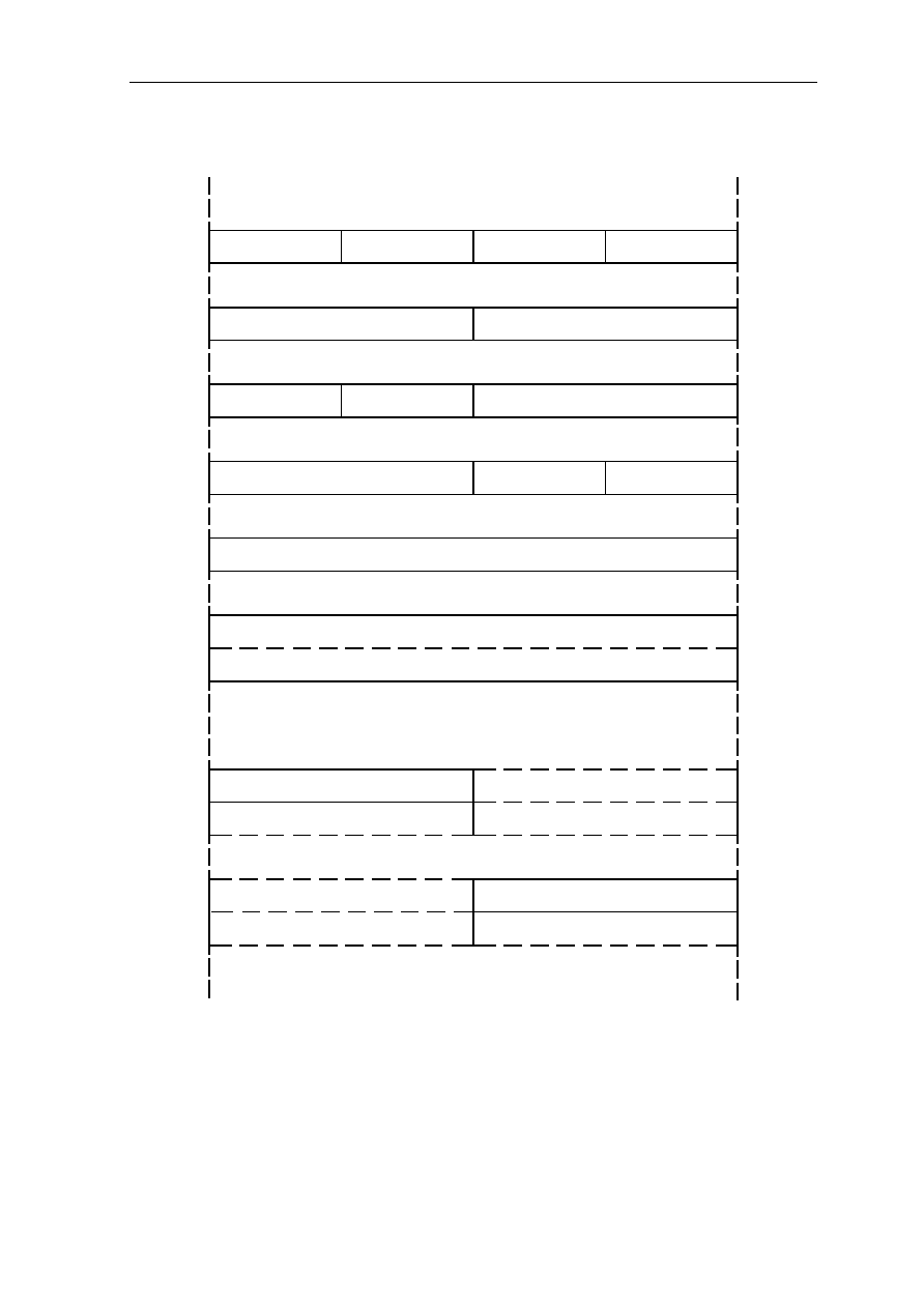
ARCHITECTURE 1-19
Figure 1.12 shows the location of data and instructions in memory relative to a binary
address n = ...xxx00 (x = 0 or 1). The memory organization is big-endian.
31
Byte n
Byte n + 1
Byte n + 2
Byte n + 3
0
Halfword n
Halfword n + 2
Byte n
Byte n + 1
Halfword n + 2
Halfword n
Byte n + 2
Byte n + 3
Word n
High-Order Word n of Double-Word
Low-Order Word n + 4 of Double-Word
1st Instruction Halfword
2nd Instruction Halfword (opt.)
3rd Instruction Halfword (opt.)
Preceding Instruction
1st Instruction Halfword
2nd Instruction Halfword (opt.)
3rd Instruction Halfword (opt.)
Figure 1.12: Memory Organization
At all data types, the most significant bit is located at the higher and the least significant bit
at the lower bit position.

1-20 CHAPTER 1
1.7 Stack
A runtime stack, called stack here, holds generations of local variables in last-in-first-out
(LIFO) order. A generation of local variables, called stack frame or activation record, is
created upon subprogram entry and released upon subprogram return.
The runtime stack provided by the architecture is divided into a memory part and a register
part. The register part of the stack, implemented by a set of 64 local registers organized as
a circular buffer, holds the most recent stack frame(s). The current stack frame is always
kept in the register part of the stack. The frame pointer FP points to the beginning of the
current stack frame (addressed as register L0). The frame length FL indicates the number
of registers (maximum 16) assigned to the current stack frame. The stack grows from low
to high address. It is guarded by the upper stack bound UB.
The stack is maintained as follows:
·
A Call, Trap or Software instruction increments the FP and sets FL to six, thus creating
a new stack frame with a length of six registers (including the return PC and the return
SR).
·
An exception increments the FP by the value of FL and then sets FL to two.
·
A Frame instruction restructures a stack frame to include (optionally) passed parameters
by decrementing the FP and by resetting the FL to the desired length, and restores a re-
serve of 10 local registers for the next subprogram call. If the required number of
registers + 10 do not fit in the register part of the stack, the contents of the differential
(required + 10 - available) number of local registers are pushed onto the memory part of
the stack. A trap to Frame Error occurs after the push operation when the old value of
the stack pointer SP exceeded the upper stack bound UB. The passed parameters are
located from L0 to the required number of register to be saved passed parameters.
Note: A Frame instruction must be executed before executing any other Call, Trap or
Software instruction or before the interrupt-lock flag L is being cleared, otherwise the
beginning of the register part of the stack at the FP could be overwritten without any
warning.
·
A Return instruction releases the current stack frame and restores the preceding stack
frame. If the restored stack frame is not fully contained in the register part of the stack,
the content of the missing part of the stack frame is pulled from the memory part of the
stack.
For more details see the descriptions of the specific instructions.
When the number of local registers required for a stack frame exceeds its maximum length
of 16 (in rare cases), a second runtime stack in memory may be used. This second stack is
also required to hold local record or array data.
The stack is used by routines in user or supervisor state, that is, supervisor stack frames are
appended to user stack frames, and thus, parameters can be passed between user and
supervisor state. A small stack space must be reserved above UB. UB can then be set to a
higher value by the Frame Error handler to free stack space for error handling.
Because the complete stack management is accomplished automatically by the hardware,
programming the stack handling instructions is easy and does not require any knowledge
of the internal working of the stack.

ARCHITECTURE 1-21
The following example demonstrates how the Call, Frame and Return instructions are
applied to achieve the stack behavior of the register part of the stack shown in the figures
1.13
and
1.14
. Figure 3.13 shows the creation and release of stack frames in the register
part of the stack.
Program Example:
A: FRAME L13, L3 ; set frame length FL = 13, decrement FP by 3
: ; parameters passed to A can be addressed
: ; in L0, L1, L2
:
:
code of function A
:
:
MOV L7, L5 ; copy L5 to L7 for use as parameter1
MOVI L8, 4 ; set L8 = 4 for use as parameter2
CALL L9, 0, B ; call function B,
: ; save return PC, return SR in L9, L10
:
:
MOVI L0, 20 ; set L0 = 20 as return parameter for caller
RET PC, L3 ; return to function calling A,
; restore frame of caller
B: FRAME L11, L2 ; set frame length FL = 11, decrement FP by 2
: ; passed parameter1 can now be addressed in L0
: ; passed parameter2 can now be addressed in L1
:
:
code of function B
:
:
RET PC, L2 ; return to function A, frame A is restored by
; copying return PC and return SR in L2 and L3
; of frame B to PC and SR
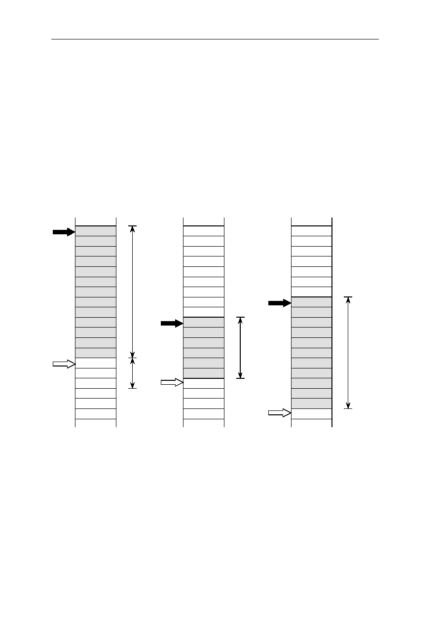
1-22 CHAPTER 1
Figure 1.13 shows the creation and release of stack frames in the register part of stack
Return from B Call B Frame in B
PC := ret. PC for B; PC := branch address; FP := FP - code of source reg.;
SR := ret. SR for B; ret. PC for B := old PC; FL := code of dest.reg.;
-- returns preceding stack frame ret. SR for B := old SR; if available registers
if stack frame contained FP := FP + reg.code (required + 10) registers then
in local registers then of ret. PC; next instruction
next instruction; FL := 6; else
else -- reg.code of ret. PC = 9 push contents of
pull contents of differential words differential number of
from memory part of the stack; registers to memory
part of stack;
-- code of source reg. = 2
-- code of dest.reg. = 11
L0
L1
L2
L3
L4
L5
L6
L7
L8
L9
L10
L11
L12
L13
L14
L15
Frame
Pointer
(FP)
current
length
of
frame A
FL = 13
parameters
for
must not
be used
FP+FL
L0
L1
L2
L3
L4
L5
New
FP
current
length
of
frame B
FL = 6
parameters
for frame B
ret. PC for A
ret. SR for A
reserved
for
maximum
number of
variables
in frame A
ret. PC for B
ret. SR for B
FP+FL
reserved for
max. number
of variables
in frame B
parameters
for
ret. PC for A
ret. SR for A
New
FP
current
length
of
frame B
FL = 11
parameters
for frame B
ret. PC for B
ret. SR for B
FP+FL
parameters
for
ret. PC for A
ret. SR for A
reserved
for
maximum
number of
variables
in frame B
L0
L1
L2
L3
L4
L5
L6
L7
L8
L9
L10
frame A
frame A
frame A
before Call B and after CALL L9, 0, dest; after FRAME L11, L2
after Return
Figure 1.13: Stack frame handling (register part)

ARCHITECTURE 1-23
A currently activated function A has a frame length of FL = 13, FL = 3(required to save passed
parameters) + 10(received). Registers L0..L6 are to be retained through a subsequent call,
registers L7..L12 are temporaries. A call to function B needs 2 parameters to be passed. The
parameters are placed by function A in registers L7 and L8 before calling B. The Call instruction
addresses L9 as destination for the return PC and return SR register pair to be used by function B
on return to function A.
On entry of function B, the new frame of B has an implicit length of FL = 6. It starts
physically at the former register L9 of frame A. However, since the frame pointer FP has
been incremented by 9 by the Call instruction, this register location is now being addressed
as L0 of frame B. The passed parameters cannot be addressed because they are located
below the new register L0 of frame B. To make them addressable, a Frame instruction
decrements the frame pointer FP by 2. Then, parameter 1 and 2 passed to B can be
addressed as registers L0 and L1 respectively. Note that the return PC is now to be
addressed as L2!
The Frame instruction in B specifies also the new, complete frame length FL = 11
(including the passed parameters as well as the return PC and return SR pair). Besides, a
new reserve of 10 registers for subsequent function calls and traps is provided in the
register stack. A possible overflow of the register stack is checked and handled
automatically by the Frame instruction. A program needs not and must not pay attention to
register stack overflow.
At the end of function B, a Return instruction returns control to function A and restores the
frame A. A possible underflow of the register stack is handled also automatically; thus, the
frame A is always completely restored, regardless whether it was wholly or partly pushed
into the memory part of the stack before (in the case when B called other functions).
In the present example with the frame length of FL = 13, any suitable destination register
up to L13 could be specified in the Call instruction. The parameters to be passed to the
function B would then be placed in L11 and L12. It is even possible to append a new frame
to a frame with a length of FL = 16 (coded as FL = 0 in the status register SR): the
destination register in the Call instruction is then coded as L0, but interpreted as the
register past L15.
See also
sections 3.27. Call instruction
,
3.29. Frame instruction
and
3.30. Return
instruction
for further details.
Note: With an average frame length of 8 registers, ca. 7..8 Frame instructions succeed a
pulling Return instruction until a push occurs and 7..8 Return instructions succeed a
pushing Frame instruction until a pull occurs. Thus, the built-in hysteresis makes pushing
and pulling a rare event in regular programs!
Figure 3.14 represents the stack frame pushing and popping. When the register part of the
stack A and X overlapped modulo 64 (the register part of stack was full), the frame
instruction for frame X pushed the number of words in frame A to the memory part of the
stack according to the space required for frame X. When the process returned to frame A,
the return instruction pulled the number of words form the memory part of the stack to the
register part of the stack.
1-24 CHAPTER 1
register part
of the stack
A and X
overlap modulo 64
memory part
of the stack
register part
of the stack
memory part
of the stack
before Frame Instruction for frame
X
after Frame Instruction for frame
X
A
words
to be
pushed
X
additional
space for X
required
pushed number
of words
according to
space required
for frame X
stack
space
appended
before Return Instruction to frame A
after Return Instruction to frame A
frame
words for A
required
words
to be
overwritten
words
to be
pulled
pulled number
of words
completes
stack frame A!
frame
words
pulled
stack
space
freed
FP
SP
FP
additional
space for X
available
SP
A
X
FP
SP
SP
FP
stack
space
required
rest of frame A
various
frames
various
frames
rest of frame A
space
available for X
rest of frame A
various
frames
A
rest of frame A
various
frames
= available part of a frame
Figure 1.14: Stack frame pushing and popping

ARCHITECTURE 1-25
1.8 Instruction Cache
The instruction cache is transparent to programs. A program executes correctly even if it
ignores the cache, whereby it is assumed that a program does not modify the instruction
code in the local range contained in the cache.
The instruction cache holds a total of up to 128 bytes (32 unstructured 32-bit words of
instructions). It is implemented as a circular buffer that is guarded by a look-ahead counter
and a look-back counter. The look-ahead counter holds the highest and the look-back
counter the lowest address of the instruction words available in the cache. The cache-mode
flag M is used to optimize special cases in loops (see details below). The cache can be
regarded as a temporary local window into the instruction sequence, moving along with
instruction execution and being halted by the execution of a program loop.
Its function is as follows:
The prefetch control loads unstructured 32-bit instruction words (without regard to
instruction boundaries) from memory into the cache. The load operation is pipelined to a
depth of two stages (see section
3.1. Memory Instructions
for details of the load pipeline).
The look-ahead counter is incremented by four at each prefetch cycle. It always contains
the address of the last instruction word for which an address bus cycle is initiated,
regardless of whether the addressed instruction word is in the load pipeline or already
loaded into the instruction cache.
The prefetched instruction word is placed in the cache word location addressed by bits 6..2
of the look-ahead counter. The look-back counter remains unchanged during prefetch
unless the cache word location it addresses with its bits 6..2 is overwritten by a prefetched
instruction word. In this case, it is incremented by four to point to the then lowest-
addressed usable instruction word in the cache. Since the cache is implemented as a
circular buffer, the cache word addresses derived from bits 6..2 of the look-ahead and look-
back counter wrap around modulo 32.
The prefetch is halted:
·
When eight words are prefetched, that is, eight words are available (including those
pending in the load pipeline) in the prefetch sequence succeeding the instruction word
addressed by the program counter PC through the instruction word addressed by the
look-ahead counter. Prefetch is resumed when the PC is advanced by instruction
execution.
·
In the cycle preceding the execution cycle of an instruction accessing memory or I/O or
any potentially branch-causing instruction (regardless of whether the branch is taken)
except a forward Branch or Delayed Branch instruction with an instruction length of one
halfword and a branch target contained in the cache. Halting the prefetch in these cases
avoids filling the load pipeline with demands for potentially unnecessary instruction
words. The prefetch is also halted during the execution cycle of any instruction
accessing memory or I/O.
The cache is read in the decode cycle by using bits 6..1 of the PC as an address to the first
halfword of the instruction presently being decoded. The instruction decode needs and uses
only the number (1, 2 or 3) of instruction halfwords defined by the instruction format.
Since only the bits 6..1 of the PC are used for addressing, the halfword addresses wrap
around modulo 64. Idle wait cycles are inserted when the instruction is not or not fully
available in the cache.

1-26 CHAPTER 1
At an explicit Branch or Delayed Branch instruction (except when placed as delay
instruction) with an instruction length of one halfword, the location of the branch target is
checked. The branch target is treated as being in the cache when the target address of a
backward branch is not lower than the address in the look-back counter and the target
address of a forward branch is not higher than two words above the address in the look-
ahead counter. That is, the two instruction words succeeding the instruction word
addressed by the content of the look-ahead counter are treated by a forward branch as
being in the cache. Their actual fetch overlaps in most cases with the execution of the
branch instruction and thus, no cycles are wasted. When the branch target is in the cache,
the look-back counter and the look-ahead counter remain unchanged.
When a branch is taken by a Delayed Branch instruction with an instruction length of one
halfword to a forward branch target not in the cache and the cache mode flag M is enabled
(1), the look-back counter and the look-ahead counter remain unchanged. Wait cycles are
then inserted until the ongoing prefetch has loaded the branch target instruction into the
cache.
Any other branch taken flushes the cache by placing the branch address in the look-back
and the look-ahead counter. Prefetch then starts immediately at the branch address.
Instruction decoding waits until the branch target instruction is fully available in the cache.
The cache mode flag M (bit four of the SR) can be set or cleared by logical instructions. It
is automatically cleared by a Frame instruction and by any branch taken except a branch
caused by a Delayed Branch or Return instruction; a Delayed Branch instruction leaves the
M flag unchanged and a Return instruction restores the M flag from the saved status
register SR.
Note: Since up to eight instruction words can be loaded into the cache by the prefetch, only
24 instruction words are left to be contained in a program loop. Thus, a program loop can
have a maximum length of 96 or 94 bytes including the branch instruction closing the loop,
depending on the even or odd halfword address location of the first instruction of the loop
respectively.
A forward Branch or Delayed Branch instruction with an instruction length of one
halfword into up to two instruction words succeeding the word addressed by the look-
ahead counter treats the branch target as being in the cache and does not flush the cache.
Thus, three or four instruction halfwords, depending on the odd or even halfword address
location of the branch instruction respectively, can always be skipped without flushing the
cache.
Enabling the cache-mode flag M is only required when a program loop to be contained in
the cache contains a forward branch to a branch target in the program loop and more than
three (or four, see above) instruction halfwords are to be skipped. In this case, the enabled
M flag in combination with a Delayed Branch instruction with an instruction length of one
halfword inhibits flushing the cache when the branch target is not yet prefetched.

ARCHITECTURE 1-27
Since a single-word memory instruction halts the prefetch for two cycles, any sequence of
memory instructions, even with interspersed one-cycle non-memory instructions, halts the
prefetch during its execution. Thus, alternating between instruction and data memory pages
is avoided. If the number of instruction halfwords required by such a sequence is not
guaranteed to be in the cache at the beginning of the sequence, a Fetch instruction
enforcing the prefetch of the sequence may be used. A Fetch instruction may also be used
preceding a branch into a program loop; thus, flushing the cache by the first branch
repeating the loop can be avoided.
A branch taken caused by a Branch or Delayed Branch instruction with an instruction
length of two halfwords always flushes the instruction cache, even if the branch target is in
the cache. Thus, branches can be forced to bypass the cache, thereby reducing the cache to
a prefetch buffer. This reduced function can be used for testing.
1.9 On-Chip Memory (IRAM)
8KBytes of memory are provided on-chip. The on-chip-memory (IRAM) is mapped to the
hex address C000 0000 of the memory address space and wraps around modulo 8K up to
DFFF FFFF. The IRAM is implemented as dynamic memory, needing refresh (DRAM).
The refresh rate must be specified in the MCR bits 18..16
(see section 6.4. Memory
Control Register MCR)
before any use (default is refresh disabled). The number given in
MCR(18..16) specifies the refresh rate in CPU clock cycles; e.g. 128 specifies a refresh
cycle automatically inserted every 128 clock cycles. Each refresh cycle refreshes 16 bytes,
thus, 256 refresh cycles are required to refresh the whole IRAM. A high refresh rate does
not degrade performance since the refresh cycles are inserted on idle IRAM cycles
whenever possible.
An access to the IRAM bypasses the access pipeline of the external memory. Thus,
pending external memory accesses do not delay accesses to the IRAM. The IRAM can
hold data as well as instructions. Instruction words from the IRAM are automatically
transferred to the instruction cache on demand; these transfers do not interfere with
external memory accesses. Besides bypassing of the external memory pipeline, memory
instructions accessing the IRAM behave exactly alike those accessing external memory.
The minimum delay for a load access is one cycle; that is, the data is not available in the
cycle after the load instruction. One or more wait cycles are automatically inserted if the
target register of the load is addressed before the data is loaded into the target register.
Attention: For selection between an internal and external memory access, bits
31..29 of the specified address register are used before calculation of the effective
address. Therefore, the content of the specified address register must point into
the IRAM address range. The IRAM address range boundary must not be crossed
when the effective memory address is calculated in the displacement address
mode.


Instruction General 2-1
2. Instructions General
2.1 Instruction Notation
In the following instruction-set presentation, an informal description of an instruction is
followed by a formal description in the form:
Format Notation Operation
Format denotes the instruction format.
Notation gives the assembler notation of the instruction.
Operation describes the operation in a Pascal-like notation with the following symbols:
Ls denotes any of the local registers L0..L15 used as source register or as source
operand. At memory Load instructions, Ls denotes the load destination register.
Ld denotes any of the local registers L0..L15 used as destination register or as
destination operand.
Rs denotes any of the local registers L0..L15 or any of the global registers G0..G15
used as source register or as source operand. At memory Load, see Ls.
Rd denotes any of the local registers L0..L15 or any of the global registers G0..G15
used as destination register or as destination operand.
Lsf, Ldf, Rsf and Rdf denote the register or operand following after (with a register address
one higher than) Ls, Ld, Rs and Rd respectively.
imm, const, dis, lim, rel, adr and n denote immediate operands (constants) of various
formats and ranges.
Operand(x) denotes a single bit at the bit position x of an operand.
Example: Ld(31) denotes bit 31 of Ld.
Operand(x..y) denotes bits x through y of an operand.
Example: Ls(4..0) denotes bits 4 through 0 of Ls.
Expression^ denotes an operand at a location addressed by the value of the expression.
Depending on the context, the expression addresses a memory location or a local
register.
Example: Ld^ denotes a memory operand whose memory address is the operand Ld.
(FP + FL)^ denotes a local register operand whose register address is FP + FL.
: = signifies the assignment symbol, read as "is replaced by".
// signifies the concatenation symbol. It denotes concatenation of two operand words
to a double-word operand or concatenation of bits and bitstrings.
Examples: Ld//Ldf denotes a double-word operand, 16 zeros//imm1 denotes
expanding of an immediate half-word by 16 leading zeros.
=,
, > and < denote the equal, unequal, greater than and less than relations.
Example: The relation Ld = 0 evaluates to one if Ld is equal to zero, otherwise it
evaluates to zero.

3-2 CHAPTER 3
2.2 Instruction Execution
On instruction execution, all bits of the operands participate in the operations, except on
the Shift and Rotate instructions (whereat only the 5 least significant bits of the source
operand are used) and except on the byte and half-word Store instructions.
Instruction pipeline is as follows:
Instructions are executed by a two-stage pipeline. In the first stage, the instruction is
fetched from the instruction cache and decoded. In the second stage, the instruction is
executed while the next instruction in the first stage is already decoded.
Register instructions are as follows:
On register instructions executing in one or two cycles, the corresponding source and
destination operand words are read from their registers and evaluated in each cycle in
which they are used. Then the result word is placed in the corresponding destination
register in the same cycle. Thus, on all single-word register instructions executing in one
cycle, the source operand register and the destination operand register may coincide
without changing the effect of the instruction. On all other instructions, the effect of a
register coincidence depends on execution order and must be examined specifically for
each such instruction.
The content of a source register remains unchanged unless it is used coincidentally as a
destination register (except on memory Load instructions).
Conditional flags are changed:
Some instructions set or clear condition flags according to the result and special conditions
occurring during their execution. The conditions may be expressed by single bits, relations
or logical combinations of these. If a condition evaluates to one (true), the corresponding
condition flag is set to one, if it evaluates to zero (false), the corresponding condition flag
is cleared to zero. A trap to Range Error may occur if the specific flags and the destination
are updated.
All instructions may use the result and any flags updated by the preceding instruction. A
time penalty occurs only if the result of a memory Load instruction is not yet available
when needed as destination or source operand. In this case one or more (depending on the
memory access time) idle wait cycles are enforced by a hardware interlock.
Using local registers are as follows:
An instruction must not use any local register of the register sequence beginning with L0
beyond the number of usable registers specified by the current value of the frame length
FL (FL = 0 is interpreted as FL = 16). That is, the value of the corresponding register code
(0..15) addressing a local register must be lower than the interpreted value of the FL
(except with a Call or Frame instruction or some restricted cases). Otherwise, an exception
could overwrite the contents of such a register or the beginning of the register part of the
stack at the SP could be overwritten without any warning when a result is placed in such a
register.
Double-word instructions denote the high-order word (at the lower address). The low-order
word adjacently following it (at the higher address) is implied.
"Old" denotes the state before the execution of an instruction.
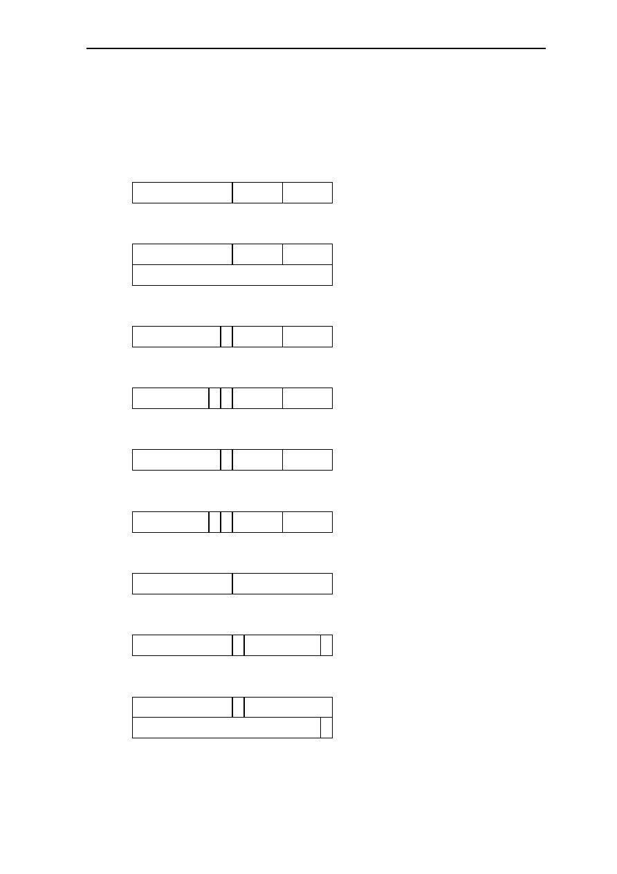
Instruction General 2-3
2.3 Instruction Formats
Instructions have a length of one, two or three half-words and must be located on half-
word boundaries. The following formats are provided:
Format
LL
LR
RR
Ln
Rn
PCadr
PCrel
PCrel
OP-code
Ld-code
Ls-code
OP-code
n Ld-code
n
OP-Code
d n Rd-code
n
OP-code
adr-byte
OP-code
0
low-rel
S
OP-code
1
high-rel
low-rel
S
9
15
8 7
4 3
0
10 9
15
8 7
4 3
0
9
15
8 7
4 3
0
15
8 7
0
Ls-code encodes L0..L15 for Ls
Ld-code encodes L0..L15 for Ld
Rs-code encodes G0..G15 for Rs
Rs-code encodes L0..L15 for Rs
Ld-code encosed L0..L15 for Ld
Rs-code encodes G0..G15 for Rs
Rs-code encodes L0..L15 for Rs
Rd-code encodes G0..G15 for Rd
Rd-code encodes L0..L15 for Rd
Ld-code encodes L0..L15 for Ld
Bit 8//bits 3..0 encode n = 0..31
Rd-code encodes G0..G15 for Rd
Rd-code encodes L0..L15 for Rd
Bit 8//bits 3..0 encode n = 0..31
adr = 24 ones's//adr-byte(7..2)//00
sign bit of rel
rel = 9 S//high-rel//low-rel//0
range -8 388 608..8 388 606
sign bit of rel
rel = 25 S//low-rel//0
range -128..126
10 9
15
8 7
4 3
0
15
8 7
0
6
1
15
8 7
0
6
1
OP-Code
d s Rd-code
Rs-code
15
8 7
4 3
0
OP-code
s Ld-code
Rs-code
Configuration
S:
S:
d = 0:
d = 1:
n:
n:
s = 0:
s = 1:
d = 0:
d = 1:
s = 0:
s = 1:
LLext
OP-code
OP-code extension
15
8
Ld-code
Ls-code
7
4 3
0
Ls-code encodes L0..L15 for Ls
Ld-code encodes L0..L15 for Ld
OP-code extension encodes the
EXTEND instructions
Table 2.1: Instruction Formats, Part 1
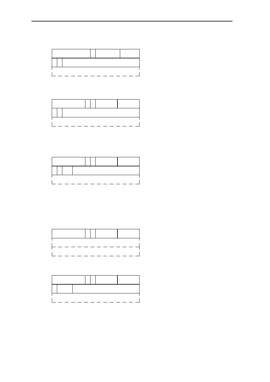
3-4 CHAPTER 3
Configuration
LRconst
RRconst
9
15
8 7
4 3
0
Rs-code encodes G0..G15 for Rs
Rs-code encodes L0..L15 for Rs
Ld-code encodes L0..L15 for Ld
Sign bit of const
const = 18 S//const1
range -16 384..16 383
const = 2 S//const1//const2
range -1 073 741 824..1 073 741 823
Rs-code encodes G0..G15 for Rs
Rs-code encodes L0..L15 for Rs
Rd-code encodes G0..G15 for Rd
Rd-code encodes L0..L15 for Rd
Sign bit of const
const = 18 S//const 1
range -16 384..16 383
const = 2 S//const1//const2
range -1 073 741 824..1 073 741 823
Rd-code encodes G0..G15 for Rd
Rd-code encodes L0..L15 for Rd
Bit 8//bits 3..0 encode n = 0..31
see Table 2.3. Encoding of
Immediate Values for encoding of
imm
10 9
15
8 7
4 3
0
d
OP-code
s
Ld-code
Rs-code
OP-code
s Rd-code
Rs-code
RRdis
10 9
15
8 7
4 3
0
d
OP-code
s Rd-code
Rs-code
Rs-code encodes G0..G15 for Rs
Rs-code encodes L0..L15 for Rs
Rd-code encodes G0..G15 for Rd
Rd-code encodes L0..L15 for Rd
Sign bit of dis
dis = 20 S//dis1
range -4 096..4 095
dis = 4 S//dis1//dis2
range -268 435 456..268 435 455
D-code, D13..D12 encode data
types at memory instructions
10 9
15
8 7
4 3
0
d
OP-code
n Rd-code
n
10 9
15
8 7
4 3
0
d
OP-code
s Rd-code
Rs-code
Rs-code encodes G0..G15 for Rs
Rs-code encodes L0..L15 for Rs
Rd-code encodes G0..G15 for Rd
Rd-code encodes L0..L15 for Rd
X-code, X14..X12 encode Index
instructions
lim = 20 zeros//lim1
range 0..4 095
lim = 4 zeros//lim1//lim2
range 0..268 435 455
14
14
14
Rimm
RRlim
e S
const1
const2
e
const1
const2
e S
S
D D
dis1
dis2
imm1
imm2
e X X X
lim1
lim2
Format
s = 0:
s = 1:
S:
e = 0:
e = 1:
s = 0:
s = 1:
d = 0:
d = 1:
S:
e = 0:
e = 1:
s = 0:
s = 1:
d = 0:
d = 1:
S:
e = 0:
e = 1:
DD:
d = 0:
d = 1:
n:
s = 0:
s = 1:
d = 0:
d = 1:
XXX:
e = 0:
e = 1:
14
Table 2.2: Instruction Formats, Part 2

Instruction General 2-5
2.3.1 Table of Immediate Values
n
immediate value
imm
Comment
0..1
6
0..16
at CMPBI, n = 0 encodes ANYBZ
at ADDI and ADDSI n = 0 encodes CZ
17
imm1//imm2
range = 0..2
32
-1 or -2
31
..2
31
-1
18
16 zeros//imm1 range = 0..65 535
19
16 ones//imm1 range = -65 536..-1
20
32
bit 5 = 1, all other bits = 0
21
64
bit 6 = 1, all other bits = 0
22
128
bit 7 = 1, all other bits = 0
23
2
31
bit 31 = 1, all other bits = 0
24
-8
25
-7
26
-6
27
-5
28
-4
29
-3
30
-2
31
2
31
-1
at CMPBI and ANDNI
bit 31 = 0, all other bits = 1
31
-1
at all other instructions using imm
Table 2.3: Encoding of Immediate Values
Note: 2
31
provides clear, set and invert of the floating-point sign bit at ANDNI, ORI and
XORI respectively.
2
31
-1 provides a test for floating-point zero at CMPBI and extraction of the sign bit at
ANDNI.
See CMPBI for ANYBZ and ADDI, ADDSI for CZ.
3-6 CHAPTER 3
2.3.2 Table of Instruction Codes
CHK, CHKZ, NOP
XMx, XMxZ
CMP
MOVD, RET
MASK
MOV
ANDN
DIVU
SUM
ADD
OR
DIVS
XOR
SUBS
ADDSI
SUB
NEG
ADDI
ORI
AND
MOVI
ANDNI
CMPI
CMPBI
SHRDI
SHR
LDxx.D/A/IOD/IOA
SHRI
FSUBD
DBE
BE
BNE
FADDD
FADD
DBNV
DBV
BNV
LD
W.
R
LDD.R
SARDI
SAR
LDxx.N/S
FDIV
FDIVD
BSE
BHT
FMUL
DBNC
DBC
BC
STxx.D/A/IOD/IOA
SHLI
FCMPUD
DBLE
BLE
BGT
FCMPD
DBNN
DBN
BNN
ST
W.
R
STD.R
ROL
STxx.N/S
MUL
EXTEND
DO
CALL
FCVTD
FCVT
FRAME
DBR
ST
W.
P
STD.P
TRAPxx, TRAP
2
3
0
6
5
4
B
9
8
D
C
F
E
OP-code Bits 11..8
A
B
C
D
E
F
OP-code Bits 15..12
Table 2.4: Table of Instruction Codes

Instruction General 2-7
2.3.3 Table of Extended DSP Instruction Codes
The Extended DSP instructions are specified by a 16-bit OP-code extension succeeding the
instruction op-code for the EXTEND instruction. See section
3.32. Extended DSP
Instructions
.
Instructio
n
OP-code
extension
(hex)
EMUL
0100
EMULU
0104
EMULS
0106
EMAC
010A
EMACD
010E
EMSUB
011A
EMSUBD
011E
EHMAC
002A
EHMACD
002E
EHCMULD
0046
EHCMAC
D
004E
EHCSUM
D
0086
EHCFFTD
0096
Table 2.5: Extended DSP Instruction Codes

3-8 CHAPTER 3
2.4 Entry Tables
Spacing of the entries for the Trap instructions and exceptions is four bytes. These entries
are intended to each contain an instruction branching to the associated function. The entries
for the TRAPxx instructions are the same as for TRAP. Table 2.6 shows the trap entries
when the entry table is mapped to the end of memory area MEM3 (default after Reset):
Address (Hex)
Entry
Description
FFFF FF00
TRAP 0
FFFF FF04
TRAP 1
:
:
FFFF FFC0
TRAP 48 IO2 Interrupt -- priority 15
FFFF FFC4
TRAP 49 IO1 Interrupt -- priority 14
FFFF FFC8
TRAP 50 INT4 Interrupt -- priority 13
FFFF FFCC
TRAP 51 INT3 Interrupt -- priority 11
FFFF FFD0
TRAP 52 INT2 Interrupt -- priority 9
FFFF FFD4
TRAP 53 INT1 Interrupt -- priority 7
FFFF FFD8
TRAP 54 IO3 Interrupt -- priority 5
FFFF FFDC
TRAP 55 Timer Interrupt -- priority selectable as 6, 8, 10, 12
FFFF FFE0
TRAP 56 Reserved -- priority 17 (lowest)
FFFF FFE4
TRAP 57 Trace Exception -- priority 16
FFFF FFE8
TRAP 58 Parity Error -- priority 4
FFFF FFEC
TRAP 59 Extended Overflow -- priority 3
FFFF FFF0
TRAP 60 Range, Pointer, Frame and Privilege Error -- priority 2
FFFF FFF4
TRAP 61 Reserved -- priority 1
FFFF FFF8
TRAP 62 Reset -- priority 0 (highest)
FFFF FFFC
TRAP 63 Error entry for instruction code of all ones
Table 2.6: Trap entry table mapped to the end of MEM3

Instruction General 2-9
Table 2.7 shows the trap entries when the entry table is mapped to the beginning of
memory areas MEM0, MEM1, MEM2 or IRAM. x is 0, 4, 8 or C corresponding to the
mapping to MEM0, MEM1, MEM2 or IRAM respectively.
Address (Hex)
Entry
Description
x000 0000
TRAP 63 Error entry for instruction code of all ones
x000 0004
TRAP 62 Reset -- priority 0 (highest)
x000 0008
TRAP 61 Reserved -- priority 1
x000 000C
TRAP 60 Range, Pointer, Frame and Privilege Error -- priority 2
x000 0010
TRAP 59 Extended Overflow -- priority 3
x000 0014
TRAP 58 Parity Error -- priority 4
x000 0018
TRAP 57 Trace Exception -- priority 16
x000 001C
TRAP 56 Reserved -- priority 17 (lowest)
x000 0020
TRAP 55 Timer Interrupt -- priority selectable as 6, 8, 10, 12
x000 0024
TRAP 54 IO3 Interrupt -- priority 5
x000 0028
TRAP 53 INT1 Interrupt -- priority 7
x000 002C
TRAP 52 INT2 Interrupt -- priority 9
x000 0030
TRAP 51 INT3 Interrupt -- priority 11
x000 0034
TRAP 50 INT4 Interrupt -- priority 13
x000 0038
TRAP 49 IO1 Interrupt -- priority 14
x000 003C
TRAP 48 IO2 Interrupt -- priority 15
:
:
x000 00F8
TRAP 1
x000 00FC TRAP
0
Table 2.7: Trap entry table mapped to the beginning of MEM0, MEM1, MEM2 or IRAM

3-10 CHAPTER 3
Table 2.8 below shows the addresses of the first instruction of the emulator code associated
with the floating-point instructions when the trap entry tables are mapped to the end of
memory area MEM3. Spacing of the entries for the Software instructions FADD..DO is 16
bytes.
Address (Hex) Entry
Description
FFFF FE00
FADD
Floating-point Add, single word
FFFF FE10
FADDD
Floating-point Add, double-word
FFFF FE20
FSUB
Floating-point Subtract, single word
FFFF FE30
FSUBD
Floating-point Subtract, double-word
FFFF FE40
FMUL
Floating-point Multiply, single word
FFFF FE50
FMULD
Floating-point Multiply, double-word
FFFF FE60
FDIV
Floating-point Divide, single word
FFFF FE70
FDIVD
Floating-point Divide, double-word
FFFF FE80
FCMP
Floating-point Compare, single word
FFFF FE90
FCMPD
Floating-point Compare, double-word
FFFF FEA0
FCMPU
Floating-point Compare Unordered, single word
FFFF FEB0
FCMPUD Floating-point Compare Unordered, double-word
FFFF FEC0
FCVT
Floating-point Convert single word
double-word
FFFF FED0
FCVTD
Floating-point Convert double-word
single word
FFFF FEE0
Reserved
FFFF FEF0
DO
Do instruction
Table 2.8: Floating-Point entry table mapped to the end of MEM3

Instruction General 2-11
Table 2.9 below shows the addresses of the first instruction of the emulator code associated
with the floating-point instructions when the trap entry tables are mapped to the beginning
of memory areas MEM0, MEM1, MEM2 or IRAM. x is 0, 4, 8 or C corresponding to the
mapping to MEM0, MEM1, MEM2 or IRAM respectively.
Address (Hex) Entry
Description
x000 010C
DO
Do instruction
x000 011C
Reserved
x000 012C
FCVTD
Floating-point Convert double-word
single word
x000 013C
FCVT
Floating-point Convert single word
double-word
x000 014C
FCMPUD Floating-point Compare Unordered, double-word
x000 015C
FCMPU
Floating-point Compare Unordered, single word
x000 016C
FCMPD
Floating-point Compare, double-word
x000 017C
FCMP
Floating-point Compare, single word
x000 018C
FDIVD
Floating-point Divide, double-word
x000 019C
FDIV
Floating-point Divide, single word
x000 01AC
FMULD
Floating-point Multiply, double-word
x000 01BC
FMUL
Floating-point Multiply, single word
x000 01CC
FSUBD
Floating-point Subtract, double-word
x000 01DC
FSUB
Floating-point Subtract, single word
x000 01EC
FADDD
Floating-point Add, double-word
x000 01FC
FADD
Floating-point Add, single word
Table 2.9: Floating-Point entry table mapped to the beginning of MEM0, MEM1, MEM2 or IRAM

3-12 CHAPTER 3
2.5 Instruction Timing
The following execution times are given in number of processor clock cycles.
All instructions not shown below: 1 cycle
Move Double-Word: 2 cycles
Shift Double-Word: 2 cycles
Test Leading Zeros: 2 cycles
Multiply word:
when both operands are in the range of -2
15
..2
15
-1: 4 cycles
all other cases: 5 cycles
Multiply double-word signed:
when both operands are in the range of -2
15
..2
15
-1: 5 cycles
all other cases: 6 cycles
Multiply double-word unsigned:
when both operands are in the range of 0..2
16
-1: 4 cycles
all other cases: 6 cycles
Divide unsigned and signed: 36 cycles
Branch instructions when branch not taken: 1 cycle
when branch taken and target in on-chip cache: 2 cycles
when branch taken and target in memory : 2 + memory read latency cycles
(see next page)
Delayed Branch instructions when branch not taken: 1 cycle
when branch taken and target in on-chip cache: 1 cycle
when branch taken and target in memory: 1 + memory read latency cycles exceeding
(delay instruction cycles - 1)
Call and Trap instructions when branch not taken: 1 cycle
when branch taken: 2 + memory read latency cycles
Software instructions: 6 + memory read latency cycles exceeding 4 cycles
Frame when not pushing words on the stack: 3 cycles
additionally when pushing n words on the stack: memory write latency cycles
+ n * bus cycles per access
-- write latency = cycles elapsed until write access cycle of first word stored
(minimum = 1 at a non-RAS access and no pipeline congestion)
Return:
4 + memory read latency cycles exceeding 2 cycles
additionally when pulling n words from the stack: memory RAS latency
+ n * bus cycles per access
(RAS latency applies only at n > 2, otherwise RAS latency is always 0)
-- RAS latency = RAS precharge cycles + RAS to CAS delay cycles

Instruction General 2-13
Fetch instruction:
when the required number of instruction half-words is already prefetched in the
instruction cache: 1 cycle
otherwise
1 + (required number of half-words - number of half-words already prefetched)/2
* bus cycles per access
Memory word instructions, non-stack address mode:
1 cycle
Memory word instructions, stack address mode:
3 cycles
Memory double-word instructions:
2 cycles
For timing calculations, double-word memory instructions are treated like a sequence of
two single-word memory instructions.
Idle wait cycles are transparently inserted when a memory instruction has to wait for
execution because the two-stage address pipeline is full.
Instruction execution proceeds after the execution of a Load instruction until the data
requested is needed (that is, the register into which the data is to be loaded is addressed) by
a further instruction.
The cycles executed between the memory instruction cycle requesting the data and the first
cycle at which the data are available are called read latency cycles. These read latency
cycles can be filled with instructions that do not need the requested data. When, after the
execution of these optional fill instruction cycles, the data is still not available in the cycle
needing it, idle wait cycles are inserted until the data is available. The idle wait cycles are
inserted transparently to the program by an on-chip hardware interlock. The read latency
is:
On an IRAM access:
read latency = 1 cycle
On a non-RAS external memory or I/O access:
read latency = address setup cycles + access cycles + 1
On a RAS memory access:
read latency = RAS precharge cycles + RAS to CAS delay cycles +
access cycles + 1
Additional cycles are also inserted and add to the latency when the address pipeline is
congested, these cycles must then also be taken into calculation.
A switch from an external memory or I/O read access to an immediately succeeding writes
access inserts one additional bus cycle.
Extended DSP instructions:
The instruction issue time is always 1 cycle. After the issue of an Extended DSP
instruction, execution of non-Extended-DSP instructions proceeds while the Extended DSP
instruction is executed in the multiply/accumulate unit (using separate resources). Latency
cycles are defined as the interval between instruction issue and the result being available in
the register G15 or register pair G14//G15. The latency cycles indicate as well the number
of cycles available for instructions not using the result that can be inserted between the

3-14 CHAPTER 3
Extended DSP instruction and the first instruction using the result. When less than the
number of latency cycles are used by these instructions, the execution of the instruction
using the result is delayed until the result is available in G15 or G14//G15.
When an Extended DSP instruction that uses the internal hardware multiplier (EMUL, ...,
EHCMACD) succeeds an Extended DSP instruction that also uses the internal hardware
multiplier after less than latency - 1 cycles, the issue of the succeeding Extended DSP
instruction is delayed until latency - 1 cycles are finished. An Extended DSP instruction
succeeding the EHCSUMD or EHCFFTD instruction after less than the latency cycles for
these two instructions is always delayed until the EHCSUMD or EHCFFTD instruction is
finished.
The latency cycles are as follows:
EMUL instruction:
when both operands are in the range of -2
15
..2
15
-1: 1 cycle
all other cases: 3 cycles
EMULU instruction:
when both operands are in the range of 0..2
16
-1: 2 cycles
all other cases: 4 cycles
EMULS instruction:
when both operands are in the range of -2
15
..2
15
-1: 3 cycles
all other cases: 4 cycles
EMAC instruction:
when both operands are in the range of -2
15
..2
15
-1: 2 cycles
all other cases: 3 cycles
EMACD instruction:
when both operands are in the range of -2
15
..2
15
-1: 3 cycles
all other cases: 4 cycles
EMSUB instruction:
when both operands are in the range of -2
15
..2
15
-1: 2 cycles
all other cases: 3 cycles
EMSUBD instruction:
when both operands are in the range of -2
15
..2
15
-1: 3 cycles
all other cases: 4 cycles
EHMAC instruction: 2 cycles
EHMACD instruction: 4 cycles
EHCMULD instruction: 4 cycles
EHCMACD instruction: 4 cycles
EHCSUMD instruction: 2 cycles
EHCFFTD instruction: 2 cycles

Instruction Set 3-1
3. Instruction Set
3.1 Memory Instructions
The memory instructions load data from memory in a register Rs (or a register pair
Rs//Rsf) or store data from Rs (or Rs//Rsf) to memory using the data types byte
unsigned/signed, half-word unsigned/signed, word or double-word. Since I/O devices are
also addressed by memory instructions, "memory" stands here interchangeably also for I/O
unless memory or I/O address space is specifically denoted.
The memory address is either specified by the operand Rd or Ld, by the sum Rd plus a
signed displacement or by the displacement alone, depending on the address mode.
Memory accesses to words and double-words ignore bits one and zero of the address,
memory accesses to half-words ignore bit zero of the address, (since these operands are
located at word or half-word boundaries respectively, these address bits are redundant).
If the content of any register Rd except SR is zero, the memory is not accessed and a trap
to Pointer Error occurs (see
section 6. Exceptions
). Thus, uninitialized pointers are
automatically checked.
Load and Store instructions are pipelined to a total depth of two word entries for Load and
Store, thus, a double-word Load or a double-word Store instruction can be executed
without halting the processor in a wait state. (The address pipeline provides a depth of two
addresses common to load and store).
Double-word memory instructions enter two separate word entries into the pipeline and
start two independent memory cycles. The first memory cycle, loading or storing the high-
order word, uses the address specified by the address mode, the second cycle uses this
address incremented by four and also places it on the address bus.
Accessing data in the same DRAM memory page by any number of succeeding memory
cycles is performed in page mode.
Memory instructions leave all condition flags unchanged.
3-2 CHAPTER 3
3.1.1 Address Modes
Register Address Mode:
Notation: LDxx.R, STxx.R -- xx: word or double word data type
The content of the destination register Ld is used as an address into memory address space.
Memory
ADDR
ADDR
DATA
DATA
Ld
Rs
LDxx.R Ld, Rs
Memory
ADDR
ADDR
DATA
DATA
Ld
Rs
STxx.R Ld, Rs
Postincrement Address Mode:
Notation: LDxx.P, STxx.P -- xx: word or double-word data type
The content of the destination register Ld is used as an address into memory address space,
then Ld is incremented according to the specified data size of a word or double-word
memory instruction by 4 or 8 respectively, regardless of any exception occurring. In the
case of a double-word data type, Ld is incremented by 8 at the first memory cycle.
Memory
ADDR
ADDR
DATA
DATA
Ld
Rs
LDxx.P Ld, Rs
ADDR + size
size= 4(word) or 8(double word)
Memory
ADDR
ADDR
DATA
DATA
Ld
Rs
STxx.P Ld, Rs
ADDR + size
size= 4(word) or 8(double word)
Displacement Address Mode:
Notation: LDxx.D, STxx.D -- xx: any data type
The sum of the contents of the destination register Rd plus a signed displacement dis is
used as an address into memory address space.
Memory
ADDR
ADDR
DATA
DATA
Rd
Rs
LDxx.D Rd, Rs, dis
ADDR + dis
Memory
ADDR
ADDR
DATA
DATA
Rd
Rs
STxx.D Rd, Rs, dis
ADDR + dis
Rd may denote any register except the SR; Rd not denoting the SR differentiates this mode
from the absolute address mode.
Instruction Set 3-3
In the case of all data types except byte, bit zero of dis is treated as zero for the calculation
of Rd + dis.
Note: Specification of the PC for Rd provides addressing relative to the address of the first
byte after the memory instruction.
Absolute Address Mode:
Notation: LDxx.A, STxx.A -- xx: any data type
The displacement dis is used as an address into memory address space. Rd must denote the
SR to differentiate this mode from the displacement address mode; the content of the SR is
not used.
Memory
dis
DATA
DATA
Rs
LDxx.A 0, Rs, dis
STxx.A 0, Rs, dis
Memory
dis
DATA
DATA
Rs
In the case of all data types except byte, address bit zero is supplied as zero.
Note: The displacement provides absolute addressing at the beginning and the end (MEM3
area) of the memory.
I/O Displacement Address Mode:
Notation: LDxx.IOD, STxx.IOD -- xx: word or double-word data type
The sum of the contents of the destination register Rd plus a signed displacement dis is
used as an address into I/O address space.
IO
ADDR
ADDR
DATA
DATA
Rd
Rs
LDxx.IOD Rd, Rs, dis
ADDR + dis
IO
ADDR
ADDR
DATA
DATA
Rd
Rs
STxx.IOD Rd, Rs, dis
ADDR + dis
Rd may denote any register except the SR; Rd not denoting the SR differentiates this mode
from the I/O absolute address mode.
Bits one and zero of dis are treated as zero for the calculation of Rd + dis.
3-4 CHAPTER 3
Execution of a memory instruction with I/O displacement address mode does not disrupt
any page mode sequence.
Note: The I/O displacement address mode provides dynamic addressing of peripheral
devices.
When on a load instruction only a byte or half-word is placed on the (lower part) of the
data bus, the higher-order bits are undefined and must be masked out before the loaded
operand is used further.
I/O Absolute Address Mode:
Notation: LDxx.IOA, STxx.IOA -- xx: word or double-word data type
The displacement dis is used as an address into I/O address space.
IO
dis
DATA
DATA
Rs
LDxx.IOA 0, Rs, dis
STxx.IOA 0, Rs, dis
IO
dis
DATA
DATA
Rs
Rd must denote the SR to differentiate this mode from the I/O displacement address mode;
the content of the SR is not used.
Address bits one and zero are supplied as zero.
Execution of a memory instruction with I/O address mode does not disrupt any page mode
sequence.
Note: The I/O absolute address mode provides code efficient absolute addressing of
peripheral devices and allows simple decoding of I/O addresses.
When on a load instruction only a byte or a half-word is placed on the (lower part) of the
data bus, the higher-order bits are undefined and must be masked out before the loaded
operand is used further.
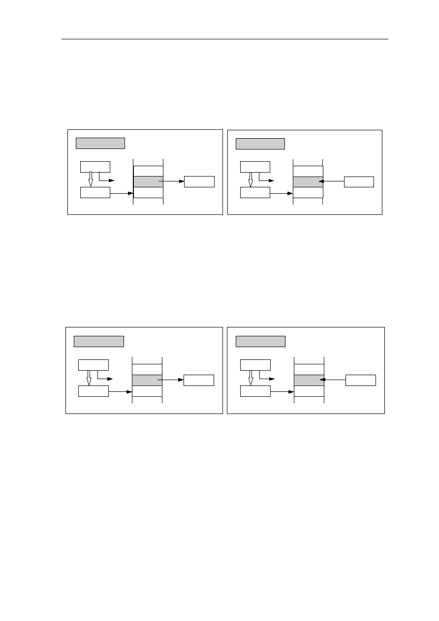
Instruction Set 3-5
Next Address Mode:
Notation: LDxx.N, STxx.N -- xx: any data type
The content of the destination register Rd is used as an address into memory address space,
then Rd is incremented by the signed displacement dis regardless of any exception
occurring. At a double-word data type, Rd is incremented at the first memory cycle.
Memory
ADDR
ADDR
DATA
DATA
Rd
Rs
LDxx.N Rd, Rs, dis
ADDR + dis
Memory
ADDR
ADDR
DATA
DATA
Rd
Rs
STxx.N Rd, Rs, dis
ADDR + dis
Rd must not denote the PC or the SR.
In the case of all data types except byte, bit zero of dis is treated as zero for the calculation
of Rd + dis.
Stack Address Mode:
Notation: LDW.S, STW.S -- only word data type
The content of the destination register Rd is used as stack address, then Rd is incremented
by dis regardless of any exception occurred.
Stack
ADDR
ADDR
DATA
DATA
Rd
Rs
LDxx.S Rd, Rs, dis
ADDR + dis
Stack
ADDR
ADDR
DATA
DATA
Rd
Rs
STxx.S Rd, Rs, dis
ADDR + dis
A stack address addresses memory address space if it is lower than the stack pointer SP;
otherwise bits 7..2 of it (higher bits are ignored) address a register in the register part of the
stack absolutely (not relative to the frame pointer FP).
Bits one and zero of dis are treated as zero for the calculation of Rd + dis.
Rd must not denote the PC or the SR.
Note: The stack address mode must be used to address an operand in the stack regardless
of its present location either in the memory part or in the register part of the stack. Rd may
be set by the Set Stack Address instruction.
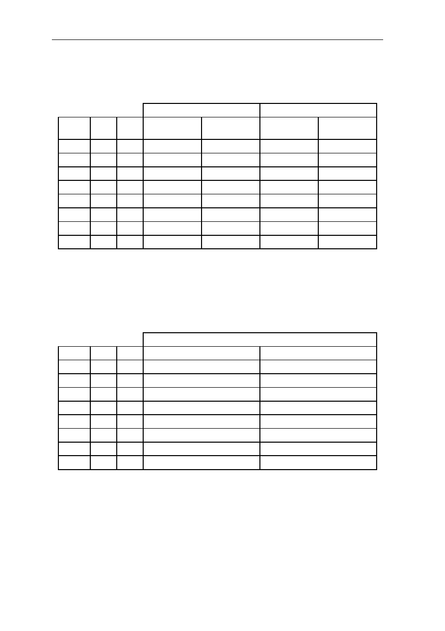
3-6 CHAPTER 3
Address Mode Encoding:
The encoding of the displacement and absolute address mode types of memory instructions
is shown in table 3.1:
LDxx.D/A/IOD/IOA
STxx.D/A/IOD/IOA
D-code dis(1) dis(0) Rd does not
denote SR
Rd denotes SR Rd does not
denote SR
Rd denotes SR
0
X
X
LDBS.D
LDBS.A
STBS.D
STBS.A
1
X
X
LDBU.D
LDBU.A
STBU.D
STBU.A
2
X
0
LDHU.D
LDHU.A
STHU.D
STHU.A
2
X
1
LDHS.D
LDHS.A
STHS.D
STHS.A
3
0
0
LDW.D
LDW.A
STW.D
STW.A
3
0
1
LDD.D
LDD.A
STD.D
STD.A
3
1
0
LDW.IOD
LDW.IOA
STW.IOD
STW.IOA
3
1
1
LDD.IOD
LDD.IOA
STD.IOD
STD.IOA
Table 3.1: Encoding of Displacement and Absolute Address Mode
The encoding of the next and stack address mode types of memory instructions is shown in
table 3.2:
With the instructions below, Rd must not denote the PC or the SR
D-code dis(1) dis(0)
LDxx.N/S
STxx.N/S
0
X
X
LDBS.N
STBS.N
1
X
X
LDBU.N
STBU.N
2
X
0
LDHU.N
STHU.N
2
X
1
LDHS.N
STHS.N
3
0
0
LDW.N
STW.N
3
0
1
LDD.N
STD.N
3
1
0
Reserved
Reserved
3
1
1
LDW.S
STW.S
Table 3.2: Encoding of Next and Stack Address Mode

Instruction Set 3-7
3.1.2 Load Instructions
The Load instructions transfer data from the addressed memory location into a register Rs
or a register pair Rs//Rsf.
In the case of data types word and double-word, one or two words are read from memory
and transferred unchanged into Rs or Rs//Rsf respectively.
In the case of byte and half-word data types, up to one word (depending on bus size) is
read from memory, the byte or half-word addressed by bits one and zero or bit one of the
memory address respectively is extracted, right adjusted, expanded to 32 bits and placed in
Rs. Unsigned bytes and half-words are expanded by leading zeros; signed bytes and half-
words are expanded by leading sign bits.
Execution of a Load instruction enters the register address of Rs, memory address bits one
and zero and a code for the data type into the load pipeline, places the memory address
onto the address bus and starts a memory cycle. A double-word Load instruction enters the
register address of Rsf and the same control information into the load pipeline as a second
entry, places the memory address incremented by four onto the address bus and starts a
second memory cycle.
After execution of a Load instruction, the next instructions are executed without waiting
for the data to be loaded. A wait is enforced only if an instruction uses a register whose
register address is still in the load pipeline. The data read from memory is placed in the
register whose register address is at the head of the load pipeline, its pipeline entry is then
deleted.
At memory load instruction Rs denotes the load destination register to load data from
memory, IO or stack and Rd denotes the load source register.
Rs must not denote the PC, the SR, G14 or G15; these registers cannot be loaded from memory.
Format Notation Operation Data Type xx
LR LDxx.R Ld, Rs Rs := Ld^; W,D
[Rsf := (Ld + 4)^;]
-- register address mode
LR LDxx.P Ld, Rs Rs := Ld^; Ld := Ld + size; -- size = 4 or 8 W,D
[Rsf := (old Ld + 4)^;]
-- postincrement address mode
RRdis LDxx.D Rd, Rs, dis Rs := (Rd + dis)^; BU,BS,HU,HS,W,D
[Rsf := (Rd + dis + 4)^;]
-- displacement address mode
RRdis LDxx.A 0, Rs, dis Rs := dis^; BU,BS,HU,HS,W,D
[Rsf := (dis + 4)^;]
-- absolute address mode
RRdis LDxx.IOD Rd, Rs, dis Rs := (Rd + dis)^; W,D
[Rsf := (Rd + dis + 4)^;]
-- I/O displacement address mode
RRdis LDxx.IOA 0, Rs, dis Rs := dis^; W,D
[Rsf := (dis + 4)^;]
-- I/O absolute address mode

3-8 CHAPTER 3
RRdis LDxx.N Rd, Rs, dis Rs := Rd^; Rd := Rd + dis; BU,BS,HU,HS,W,D
[Rsf := (old Rd + 4)^;]
-- next address mode
RRdis LDxx.S Rd, Rs, dis Rs := Rd^; Rd := Rd + dis; W
-- stack address mode
The expressions in brackets are only executed at double-word data types.
Data Type xx is with:
BU: byte unsigned; HU: half-word unsigned; W: word;
BS: byte signed; HS: half-word signed; D: double-word;
Register
L0 : $00001E30
L6 : $0000FFFF
L7 : $FFFF0000
Memory
00001E30 : 00000F00
00001E34 : 00003F01
00001E38 : 00004C10
00001E3C : 000000FF
Instruction : Register address mode
LDW.R L0, L6 ; L6 <= L0^ = Address 00001E30 : $00000F00
LDD.R L0, L6 ; L6 <= L0^ = Address 00001E30 : $00000F00
; L7 <= (L0 + 4)^ = Address 00001E34 : $00003F01
Instruction : Displacement address mode
LDW.D L0, L6, $8 ; L6 = (L0 + 8)^ = Address 00001E38 : $00004C10
LDD.D L0, L6, $8 ; L6 = (L0 + 8)^ = Address 00001E38 : $00004C10
; L7 = (L0 + 8 + 4)^ = Address 00001E3C : $000000FF

Instruction Set 3-9
3.1.3 Store Instructions
The Store instructions transfer data from the register Rs or the register pair Rs//Rsf to the
addressed memory location.
In the case of data types word or double-word, one or two words are placed unchanged
from Rs or Rs//Rsf respectively onto the data bus to be stored in the memory.
In the case of byte and half-word data types, the low-order byte or half-word is placed onto
the data bus at the byte or half-word position addressed by bits one and zero or bit one of
the memory address respectively; it is implied to be merged (via byte write enable) with
the other data in the same memory word.
In the case of signed byte and signed half-word data types, any content of Rs exceeding the
value range of the specified data type causes a trap to Range Error. The byte or half-word
is stored regardless of a Range Error.
If Rs denotes the SR, zero is stored regardless of the content of SR (or of SR//G2 at
double-word).
Execution of a Store instruction enters the contents of Rs, memory address bits one and
zero and a code for the data type into the store pipeline, places the memory address onto
the address bus and starts a memory cycle. A double-word Store instruction enters the
contents of Rsf and the same control information into the store pipeline as a second entry,
places the memory address incremented by four onto the address bus and starts a second
memory cycle.
After execution of a Store instruction, the next instructions are executed without waiting
for the store memory cycle to finish. The data at the head of the store pipeline is put on the
data bus on demand from the on-chip memory control logic and its pipeline entry is deleted.
When Rsf denotes the same register as Rd (or Ld) at double-word instructions with next
address or postincrement address mode, the incremented content of Rsf is stored in the
second memory cycle; in all other cases, the unchanged content of Rs or Rsf is stored.
Format Notation Operation Data Type xx
LR STxx.R Ld, Rs Ld^ := Rs; W,D
[(Ld + 4)^ := Rsf;]
-- register address mode
LR STxx.P Ld, Rs Ld^ := Rs; Ld := Ld + size; -- size = 4 or 8 W,D
[(old Ld + 4)^ := Rsf;]
-- postincrement address mode
RRdis STxx.D Rd, Rs, dis (Rd + dis)^ := Rs; BU,BS,HU,HS,W,D
[(Rd + dis + 4)^ := Rsf;]
-- displacement address mode
RRdis STxx.A 0, Rs, dis dis^ := Rs; BU,BS,HU,HS,W,D
[(dis + 4)^ := Rsf;]
-- absolute address mode
RRdis STxx.IOD Rd, Rs, dis (Rd + dis)^ := Rs; W,D
[(Rd + dis + 4)^ := Rsf;]
-- I/O displacement address mode

3-10 CHAPTER 3
RRdis STxx.IOA 0, Rs, dis dis^ := Rs; W,D
[(dis + 4)^ := Rsf;]
-- I/O absolute address mode
RRdis STxx.N Rd, Rs, dis Rd^ := Rs; Rd := Rd + dis; BU,BS,HU,HS,W,D
[(old Rd + 4)^ := Rsf;]
-- next address mode
RRdis STxx.S Rd, Rs, dis Rd^ := Rs; Rd := Rd + dis; W
-- stack address mode
The expressions in brackets are only executed at double-word data types.
In the case of signed byte and half-word data types, a trap to Range Error occurs when the
value of the operand to be stored exceeds the value range of the specified data type; the
byte or half-word is stored regardless of a Range Error.
Data Type xx is with:
BU: byte unsigned; HU: half-word unsigned; W: word;
BS: byte signed; HS: half-word signed; D: double-word;
Register
L0 : $00001E30
L6 : $0000FFFF
L7 : $FFFF0000
Memory
00001E30 : 00000F00
00001E34 : 00003F01
00001E38 : 00004C10
00001E3C : 000000FF
Instruction : Register address mode
STW.R L0, L6 ; L0^ = L6 = Address 00001E30 : $0000FFFF
STD.R L0, L6 ; L0^ = L6 = Address 00001E30 : $0000FFFF
; (L0 + 4)^ = L7 = Address 00001E34 : $FFFF0000
Instruction : Displacement address mode
STW.D L0, L6, $8 ; (L0 + 8)^ = L6 = Address 00001E38 : $0000FFFF
STD.D L0, L6, $8 ; (L0 + 8)^ = L6 = Address 00001E38 : $0000FFFF
; (L0 + 8 + 4)^ = L7 = Address 00001E3C : $FFFF0000

Instruction Set 3-11
3.2 Move Word Instructions
The source operand or the immediate operand is copied to the destination register and the
condition flags are set or cleared accordingly.
Format Notation Operation
RR MOV Rd, Rs Rd := Rs;
Z := Rd = 0;
N := Rd(31);
V := undefined;
Rimm MOVI Rd, imm Rd := imm;
Z := Rd = 0;
N := Rd(31);
V := 0;
3.3 Move Double-Word Instruction
The double-word source operand is copied to the double-word destination register pair and
the condition flags are set or cleared accordingly. The high-order word in Rs is copied first.
When the SR is denoted as a source operand, the source operand is supplied as zero
regardless of the content of SR//G2. When the PC is denoted as destination, the Return
instruction RET is executed instead of the Move Double-Word instruction.
Format Notation Operation
RR MOVD Rd, Rs if Rd does not denote PC and Rs does not denote SR then
Rd := Rs;
Rdf := Rsf;
Z := Rd//Rdf = 0;
N := Rd(31);
V := undefined;
RR MOVD Rd, 0 if Rd does not denote PC and Rs denotes SR then
Rd := 0;
Rdf := 0;
Z := 1;
N := 0;
V := undefined;
RR RET PC, Rs if Rd denotes PC then
execute the RET instruction;
Register
L0 : $XXXXXXXX
L1 : $XXXXXXXX
L6 : $0000FFFF
L7 : $FFFF0000
Instruction
MOV L0, L6 ; L0 = L6 = $0000FFFF
MOVI L0, $4 ; L0 = imm = $4
MOVD L0, L6 ; L0 = L6 = $0000FFFF
; L1 = L7 = $FFFF0000

3-12 CHAPTER 3
3.4 Logical Instructions
The result of a bitwise logical AND, AND not (ANDN), OR or exclusive OR (XOR) of the
source or immediate operand and the destination operand is placed in the destination
register and the Z flag is set or cleared accordingly. At ANDN, the source operand is used
inverted (itself remaining unchanged).
All operands and the result are interpreted as bitstrings of 32 bits each.
Format Notation Operation
RR AND Rd, Rs Rd := Rd and Rs; -- logical AND
Z := Rd = 0;
RR ANDN Rd, Rs Rd := Rd and not Rs; -- logical AND with source
Z := Rd = 0; used inverted
RR OR Rd, Rs Rd := Rd or Rs; -- logical OR
Z := Rd = 0;
RR XOR Rd, Rs Rd := Rd xor Rs; -- logical exclusive OR
Z := Rd = 0;
Rimm ANDNI Rd, imm Rd := Rd and not imm; -- logical AND with imm
Z := Rd = 0; used inverted
Rimm ORI Rd, imm Rd := Rd or imm; -- logical OR
Z := Rd = 0;
Rimm XORI Rd, imm Rd := Rd xor imm; -- logical exclusive OR
Z := Rd = 0;
Note: ANDN and ANDNI are the instructions complementary to OR and ORI: Where OR
and ORI set bits, ANDN and ANDNI clear bits at bit positions with a "one" bit in the
source or immediate operand, thus obviating the need for an inverted mask in most cases.
Register
L0 : $0F0CFFFF
L1 : $FFFF0000
Instruction
AND L0, L1 ; L0 = L0 and L1 = $0F0C0000
ANDN L0, L1 ; L0 = L0 and not L1 = $0000FFFF
OR L0, L1 ; L0 = L0 or L1 = $FFFFFFFF
XOR L0, L1 ; L0 = L0 xor L1 = $F0F3FFFF
ANDNI L0, $1234 ; L0 = L0 and not imm = $0F0CEDCB
ORI L0, $1234 ; L0 = L0 or imm = $0F0CFFFF
XORI L0, $1234 ; L0 = L0 xor imm = $0F0CEDCB

Instruction Set 3-13
3.5 Invert Instruction
The source operand is placed bitwise inverted in the destination register and the Z flag is
set or cleared accordingly.
The source operand and the result are interpreted as bitstrings of 32 bits each.
Format Notation Operation
RR NOT Rd, Rs Rd := not Rs;
Z := Rd = 0;
3.6 Mask Instruction
The result of a bitwise logical AND of the source operand and the immediate operand is
placed in the destination register and the Z flag is set or cleared accordingly.
All operands and the result are interpreted as bitstrings of 32 bits each.
Format Notation Operation
RRconst MASK Rd, Rs, const Rd := Rs and const;
Z := Rd = 0;
Note: The Mask instruction may be used to move a source operand with bits partly masked
out by an immediate operand used as mask. The immediate operand const is constrained in
its range by bits 31 and 30 being either both zero or both one (see format RRconst). If
these bits are required to be different, the instruction pair MOVI, AND may be used
instead of MASK.

3-14 CHAPTER 3
3.7 Add Instructions
The source operand, the source operand + C or the immediate operand is added to the
destination operand, the result is placed in the destination register and the condition flags
are set or cleared accordingly.
At ADD, ADDC and ADDI, both operands and the result are interpreted as either all
signed or all unsigned integers. At ADDS and ADDSI, both operands and the result are
signed integers and a trap to Range Error occurs at overflow.
Format Notation Operation
RR ADD Rd, Rs Rd := Rd + Rs; -- signed or unsigned Add
Z := Rd = 0;
N := Rd(31); -- sign
V := overflow;
C := carry;
RR ADDS Rd, Rs Rd := Rd + Rs; -- signed Add with trap
Z := Rd = 0;
N := Rd(31); -- sign
V := overflow;
if overflow then
trap
Range Error;
RR ADDC Rd, Rs Rd := Rd + Rs + C; -- signed or unsigned Add
Z := Z and (Rd = 0); with carry
N := Rd(31); -- sign
V := overflow;
C := carry;
When the SR is denoted as a source operand at ADD, ADDS and ADDC, C is added
instead of the SR. The notation is then:
Format Notation Operation
RR ADD Rd, C Rd := Rd + C; -- signed or unsigned Add C
RR ADDS Rd, C Rd := Rd + C; -- signed Add C with trap
RR ADDC Rd, C Rd := Rd + C;
The flags and the trap condition are treated as defined by ADD, ADDS or ADDC.

Instruction Set 3-15
Format Notation Operation
Rimm ADDI Rd, imm Rd := Rd + imm; -- signed or unsigned Add
Z := Rd = 0;
N := Rd(31); -- sign
V := overflow;
C := carry;
Rimm ADDSI Rd, imm Rd := Rd + imm; -- signed Add with trap
Z := Rd = 0;
N := Rd(31); -- sign
V := overflow;
if overflow then
trap
Range Error;
The following instructions are special cases of ADDI and ADDSI differentiated by n = 0
(see
section 2.3.1. Table of Immediate Values
):
Format Notation Operation
Rimm ADDI Rd, CZ Rd := Rd + (C and (Z = 0 or Rd(0))); -- round to even
Rimm ADDSI Rd, CZ Rd := Rd + (C and (Z = 0 or Rd(0))); -- round to even
The flags and the trap condition are treated as defined by ADDI or ADDSI.
Note: At ADDC, Z is cleared if Rd
0, otherwise left unchanged; thus, Z is evaluated
correctly for multi-precision operands.
The effect of a Subtract immediate instruction can be obtained by using the negated 32-bit
value of the immediate operand to be subtracted (except zero). At unsigned, C = 0
indicates then a borrow (the unsigned number range is exceeded below zero).
At "round to even", C is only added to the destination operand if Z = 0 or Rd(0) is one. The
Z flag is assumed to be set or cleared by a preceding Shift Left instruction. "Round to
even" provides a better averaging of rounding errors than "add carry".
"Round to even" is equivalent to the "round to nearest" Floating-Point rounding mode and
may be used to implement it efficiently.
Register
L0 : $00000004
L1 : $FFFFFFFC
Instruction
ADD L0, L1 ; L0 = L0 + L1 = $0
ADDI L0, $120 ; L0 = L0 + imm = $124

3-16 CHAPTER 3
3.8 Sum Instructions
The sum of the source operand and the immediate operand is placed in the destination
register and the condition flags are set or cleared accordingly. At SUM, both operands and
the result are interpreted as either all signed or all unsigned integers. At SUMS, both
operands and the result are signed integers and a trap to Range Error occurs at overflow.
Format Notation Operation
RRconst SUM Rd, Rs, const Rd := Rs + const; -- signed or unsigned Sum
Z := Rd = 0;
N := Rd(31); -- sign
V := overflow;
C := carry;
RRconst SUMS Rd, Rs, const Rd := Rs + const; -- signed Sum with trap
Z := Rd = 0;
N := Rd(31); -- sign
V := overflow;
if overflow then
trap
Range Error;
When the SR is denoted as a source operand at SUM and SUMS, C is added instead of the
SR. The notation is then:
Format Notation Operation
RRconst SUM Rd, C, const Rd := C + const; -- signed or unsigned Sum C
RRconst SUMS Rd, C, const Rd := C + const; -- signed Sum C
The flags are treated as defined by SUM or SUMS. A trap cannot occur.
Note: The effect of a Subtract immediate instruction can be obtained by using the negated
32-bit value of the immediate operand to be subtracted (except zero). At unsigned, C = 0
indicates then a borrow (the unsigned number range is exceeded below zero).
The immediate operand is constrained to the range of const. The instruction pair MOV,
ADDI or MOV, ADDSI may be used where the full integer range is required.
Register
L0 : $FFFFFFFC
L1 : $00000004
Instruction
SUM L0, L1, $120 ; L0 = L1 + const = $124

Instruction Set 3-17
3.9 Subtract Instructions
The source operand or the source operand + C is subtracted from the destination operand,
the result is placed in the destination register and the condition flags are set or cleared
accordingly.
At SUB and SUBC, both operands and the result are interpreted as either all signed or all
unsigned integers. At SUBS, both operands and the result are signed integers and a trap to
Range Error occurs at overflow.
Format Notation Operation
RR SUB Rd, Rs Rd := Rd - Rs; -- signed or unsigned Subtract
Z := Rd = 0;
N := Rd(31); -- sign
V := overflow;
C := borrow;
RR SUBS Rd, Rs Rd := Rd - Rs; -- signed Subtract with trap
Z := Rd = 0;
N := Rd(31); -- sign
V := overflow;
if overflow then
trap
Range Error;
RR SUBC Rd, Rs Rd := Rd - (Rs + C); -- signed or unsigned Subtract
Z := Z and (Rd = 0); with borrow
N := Rd(31); -- sign
V := overflow;
C := borrow;
When the SR is denoted as a source operand at SUB, SUBS and SUBC, C is subtracted
instead of the SR. The notation is then:
Format Notation Operation
RR SUB Rd, C Rd := Rd - C; -- signed or unsigned Subtract C
RR SUBS Rd, C Rd := Rd - C; -- signed Subtract C with trap
RR SUBC Rd, C Rd := Rd - C;
The flags and the trap condition are treated as defined by SUB, SUBS or SUBC.
Note: At SUBC, Z is cleared if Rd
0, otherwise left unchanged; thus, Z is evaluated
correctly for multi-precision operands.
Register
L0 : $124
L1 : $4
Instruction
SUB L0, L1 ; L0 = L0 - L1 = $120

3-18 CHAPTER 3
3.10 Negate Instructions
The source operand is subtracted from zero, the result is placed in the destination register
and the condition flags are set or cleared accordingly.
At NEG and NEGS, the source operand and the result are interpreted as either both signed
or both unsigned integers. At NEGS, the source operand and the result are signed integers
and a trap to Range Error occurs at overflow.
Format Notation Operation
RR NEG Rd, Rs Rd := - Rs; -- signed or unsigned Negate
Z := Rd = 0;
N := Rd(31); -- sign
V := overflow;
C := borrow;
RR NEGS Rd, Rs Rd := - Rs; -- signed Negate with trap
Z := Rd = 0;
N := Rd(31); -- sign
V := overflow;
if overflow then
trap
Range Error;
When the SR is denoted as a source operand at NEG and NEGS, C is negated instead of
the SR. The notation is then:
Format Notation Operation
RR NEG Rd, C Rd := - C; -- signed or unsigned Negate C
if C is set then
Rd := -1;
else
Rd := 0;
RR NEGS Rd, C Rd := - C; -- signed Negate C
if C is set then
Rd := -1;
else
Rd := 0;
The flags are treated as defined by NEG or NEGS. A trap cannot occur.
Register
L0 : $124
L1 : $4
Instruction
NEG L0, L1 ; L0 = - L1 = $FFFFFFFC
3.11 Multiply Word Instruction
The source operand and the destination operand are multiplied, the low-order word of the

Instruction Set 3-19
product is placed in the destination register (the high-order product word is not evaluated)
and the condition flags are set or cleared according to the single-word product.
Both operands are either signed or unsigned integers, the product is a single-word integer.
Note that the low-order word of the product is identical regardless of whether the operands
are signed or unsigned.
The result is undefined if the PC or the SR is denoted.
Format Notation Operation
RR MUL Rd, Rs Rd := low order word of product Rd
Rs;
Z := singleword product = 0;
N := Rd(31);
-- sign of singleword product;
-- valid for signed operands;
V := undefined;
C := undefined;
3.12 Multiply Double-Word Instructions
The source operand and the destination operand are multiplied, the double-word product is
placed in the destination register pair (the destination register expanded by the register
following it) and the condition flags are set or cleared according to the double-word
product.
At MULS, both operands are signed integers and the product is a signed double-word
integer. At MULU, both operands are unsigned integers and the product is an unsigned
double-word integer.
The result is undefined if the PC or the SR is denoted.
Format Notation Operation
RR MULS Rd, Rs Rd//Rdf := signed doubleword product of Rd
Rs;
Z := Rd//Rdf = 0;
-- doubleword product is zero
N := Rd(31);
-- doubleword product is negative
V := undefined;
C := undefined;
RR MULU Rd, Rs Rd//Rdf := unsigned doubleword product of Rd
Rs;
Z := Rd//Rdf = 0;
-- doubleword product is zero
N := Rd(31);
V := undefined;
C := undefined;

3-20 CHAPTER 3
Register
L0 : $5678
L1 : $1234
L2 : $9ABC
Instruction
MUL L0, L2 ; L0 = $3443B020
MULU L0, L2 ; L0 = $0
; L1 = $3443B020
3.13 Divide Instructions
The double-word destination operand (dividend) is divided by the single-word source
operand (divisor), the quotient is placed in the low-order destination register (Rdf), the
remainder is placed in the high-order destination register (Rd) and the condition flags are
set or cleared according to the quotient.
A trap to Range Error occurs if the divisor is zero or the value of the quotient exceeds the
integer value range (quotient overflow). The result (in Rd//Rdf) is then undefined. At
DIVS, a trap to Range Error also occurs and the result is undefined if the dividend is
negative.
At DIVS, the dividend is a non-negative signed double-word integer, the divisor, the
quotient and the remainder are signed integers; a non-zero remainder has the sign of the
dividend.
At DIVU, the dividend is an unsigned double-word integer, the divisor, the quotient and
the remainder are unsigned integers.
The result is undefined if Rs denotes the same register as Rd or Rdf or if the PC or the SR
is denoted.

Instruction Set 3-21
Format Notation Operation
RR DIVS Rd, Rs if Rs = 0 or quotient overflow or Rd(31) = 1 then
-- dividend is negative
Rd//Rdf := undefined;
Z := undefined;
N := undefined;
V := 1;
trap
Range Error;
else
remainder Rd, quotient Rdf := (Rd//Rdf) / Rs;
Z := Rdf = 0; -- quotient is zero
N := Rdf(31); -- quotient is negative
V := 0;
RR DIVU Rd, Rs if Rs = 0 or quotient overflow then
Rd//Rdf := undefined;
Z := undefined;
N := undefined;
V := 1;
trap
Range Error;
else
remainder Rd, quotient Rdf := (Rd//Rdf) / Rs;
Z := Rdf = 0; -- quotient is zero
N := Rdf(31);
V := 0;
Register
L0 : $1
L1 : $23456789
L2 : 123456
Instruction
DIVU L0, L2 ; L0 = $789
; L1 = $1000

3-22 CHAPTER 3
3.14 Shift Left Instructions
The destination operand is shifted left by a number of bit positions specified
at SHLI, SHLDI by n = 0..31 as a shift by 0..31;
at SHL, SHLD by bits 4..0 of the source operand as a shift by 0..31.
The higher-order bits of the source operand are ignored.
The destination operand is interpreted
at SHL and SHLI as a bitstring of 32 bits or as a signed or unsigned integer;
at SHLD and SHLDI as a double-word bitstring of 64 bits or as a signed or
unsigned double-word integer.
All Shift Left instructions insert zeros in the vacated bit positions at the right.
The double-word Shift Left instructions execute in two cycles. The low-order operand in
Ldf is shifted first. At SHLD, the result is undefined if Ls denotes the same register as Ld
or Ldf.
Format Notation Operation insert
Rn SHLI Rd, n Rd := Rd << by n; -- 0..31 zeros
Ln SHLDI Ld, n Ld//Ldf := Ld//Ldf << by n; -- 0..31 zeros
LL SHL Ld, Ls Ld := Ld << by Ls(4..0); -- 0..31 zeros
LL SHLD Ld, Ls Ld//Ldf := Ld//Ldf << by Ls(4..0); -- 0..31 zeros
The condition flags are set or cleared by all Shift Left instructions as follows:
Z := Ld = 0 or Rd = 0 on single-word;
Z := Ld//Ldf = 0 on double-word;
N := Ld(31) or Rd(31);
V := undefined
C := undefined;
Note: The symbol
<<
signifies "shifted left".
Register
L0 : $FFFF
L1 : $2
Instruction
SHLI L0, $4 ; L0 = $000FFFF0
SHL L0, L1 ; L0 = $0003FFFC

Instruction Set 3-23
3.15 Shift Right Instructions
The destination operand is shifted right by a number of bit positions specified
at SARI, SARDI, SHRI, SHRDI by n = 0..31 as a shift by 0..31.
at SAR, SARD, SHR, SHRD by bits 4..0 of the source operand as a shift by 0..31.
The higher-order bits of the source operand are ignored.
The destination operand is interpreted
at SAR and SARI as a signed integer;
at SARD and SARDI as a signed double-word integer;
at SHR and SHRI as a bitstring of 32 bits or as an unsigned integer;
at SHRD and SHRDI as a double-word bitstring of 64 bits or as an unsigned
double-word integer.
All Shift Right instructions that interpret the destination operand as signed insert sign bits,
all others insert zeros in the vacated bit positions at the left.
The double-word Shift Right instructions execute in two cycles. The high-order operand in
Ld is shifted first. At SARD and SHRD, the result is undefined if Ls denotes the same
register as Ld or Ldf.
Format Notation Operation insert
Rn SARI Rd, n Rd := Rd >> by n; -- 0..31 sign bits
Ln SARDI Ld, n Ld//Ldf := Ld//Ldf >> by n; -- 0..31 sign bits
LL SAR Ld, Ls Ld := Ld >> by Ls(4..0); -- 0..31 sign bits
LL SARD Ld, Ls Ld//Ldf := Ld//Ldf >> by Ls(4..0); -- 0..31 sign bits
Rn SHRI Rd, n Rd := Rd >> by n; -- 0..31 zeros
Ln SHRDI Ld, n Ld//Ldf := Ld//Ldf >> by n; -- 0..31 zeros
LL SHR Ld, Ls Ld := Ld >> by Ls(4..0); -- 0..31 zeros
LL SHRD Ld, Ls Ld//Ldf := Ld//Ldf >> by Ls(4..0); -- 0..31 zeros
The condition flags are set or cleared by all Shift Right instructions as follows:
Z := Ld = 0 or Rd = 0 on single-word;
Z := Ld//Ldf = 0 on double-word;
N := Ld(31) or Rd(31);
C := last bit shifted out is "one";
Note: The symbol
>>
signifies "shifted right".

3-24 CHAPTER 3
Register
L0 : $C000FFFF
L1 : $2
Instruction
SARI L0, $4 ; L0 = $FC000FFF
SAL L0, L1 ; L0 = $F0003FFF
SHRI L0, $4 ; L0 = $0C000FFF
SHL L0, L1 ; L0 = $30003FFF
3.16 Rotate Left Instruction
The destination operand is shifted left by a number of bit positions and the bits shifted out
are inserted in the vacated bit positions; thus, the destination operand is rotated. The
condition flags are set or cleared accordingly. Bits 4..0 of the source operand specify a
rotation by 0..31 bit positions; bits 31..5 of the source operand are ignored.
The destination operand is interpreted as a bitstring of 32 bits.
Format Notation Operation
LL ROL Ld, Ls Ld := Ld rotated left by Ls(4..0);
Z := Ld = 0;
N := Ld(31);
V := undefined;
C := undefined;
Note: The condition flags are set or cleared by the same rules applying to the Shift Left
instructions.
Register
L0 : $C000FFFF
L1 : $4
Instruction
ROL L0, L1 ; L0 = $000FFFFC

Instruction Set 3-25
3.17 Index Move Instructions
The source operand is placed shifted left by 0, 1, 2 or 3 bit positions in the destination
register, corresponding to a multiplication by 1, 2, 4 or 8. At XM1..XM4, a trap to Range
Error occurs if the source operand is higher than the immediate operand lim (upper bound).
All condition flags remain unchanged. All operands and the result are interpreted as
unsigned integers.
The SR must not be denoted as a source nor as a destination, nor the PC as a destination
operand; these notations are reserved for future expansion. When the PC is denoted as a
source operand, a trap to Range Error occurs if PC
lim.
X-code Format Notation Operation
0 RRlim XM1 Rd, Rs, lim Rd := Rs
1;
if Rs > lim then
trap
Range Error;
1 RRlim XM2 Rd, Rs, lim Rd := Rs
2;
if Rs > lim then
trap
Range Error;
2 RRlim XM4 Rd, Rs, lim Rd := Rs
4;
if Rs > lim then
trap
Range Error;
3 RRlim XM8 Rd, Rs, lim Rd := Rs
8;
if Rs > lim then
trap
Range Error;
4 RRlim XX1 Rd, Rs, 0 Rd := Rs
1; -- Move without flag change
5 RRlim XX2 Rd, Rs, 0 Rd := Rs
2;
6 RRlim XX4 Rd, Rs, 0 Rd := Rs
4;
7 RRlim XX8 Rd, Rs, 0 Rd := Rs
8;
Note: The Index Move instructions move an index value scaled (multiplied by 1, 2, 4 or 8).
XM1..XM4 check also the unscaled value for an upper bound, optionally also excluding
zero. If the lower bound is not zero or one, it may be mapped to zero by subtracting it from
the index value before applying an Index Move instruction.
Register
L0 : $456
L1 : $123
Instruction
XM2 L0, L1, 124 ; L0 = $246
XM2 L0, L1, 122 ; Integer Range Error in Task at Address XXXXXXXX
XX2 L0, L1, 0 ; L0 = $246

3-26 CHAPTER 3
3.18 Check Instructions
The destination operand is checked and a trap to Range Error occurs
at CHK if the destination operand is higher than the source operand,
at CHKZ if the destination operand is zero.
All registers and all condition flags remain unchanged. All operands are interpreted as
unsigned integers.
CHKZ shares its basic OP-code with CHK, it is differentiated by denoting the SR as source
operand.
Format Notation Operation
RR CHK Rd, Rs if Rs does not denote SR and Rd > Rs then
trap
Range Error;
RR CHKZ Rd, 0 if Rs denotes SR and Rd = 0 then
trap
Range Error;
When Rs denotes the PC, CHK traps if Rd
PC. Thus, CHK, PC, PC always traps. Since
CHK, PC, PC is encoded as 16 zeros, an erroneous jump into a string of zeros causes a trap
to Range Error, thus trapping some address errors.
Note: CHK checks the upper bound of an unsigned value range, implying a lower bound of
zero. If the lower bound is not zero, it can be mapped to zero by subtracting it from the
value to be checked and then checking against a corrected upper bound (lower bound also
subtracted). When the upper bound is a constant not exceeding the range of lim, the Index
instructions may be used for bounds checks.
CHKZ may be used to trap on uninitialized pointers with the value zero.
3.19 No Operation Instruction
The instruction CHK, L0, L0 cannot cause any trap. Since CHK leaves all registers and
condition flags unchanged, it can be used as a No Operation instruction with the notation:
Format Notation Operation
RR NOP no operation;
Note: The NOP instruction may be used as a fill instruction.

Instruction Set 3-27
3.20 Compare Instructions
Two operands are compared by subtracting the source operand or the immediate operand
from the destination operand. The condition flags are set or cleared according to the result;
the result itself is not retained. Note that the N flag indicates the correct compare result
even in the case of an overflow.
All operands and the result are interpreted as either all signed or all unsigned integers.
Format Notation Operation
RR CMP Rd, Rs result := Rd - Rs;
Z := Rd = Rs; -- result is zero
N := Rd < Rs signed; -- result is true negative
V := overflow;
C := Rd < Rs unsigned; -- borrow
Rimm CMPI Rd, imm result := Rd - imm;
Z := Rd = imm; -- result is zero
N := Rd < imm signed; -- result is true negative
V := overflow;
C := Rd < imm unsigned; -- borrow
When the SR is denoted as a source operand at CMP, C is subtracted instead of SR. The
notation is then:
Format Notation Operation
RR CMP, Rd, C result := Rd - C;
Z := Rd = C; -- result is zero
N := Rd < C signed; -- result is true negative
V := overflow;
C := Rd < C unsigned; -- borrow
3.21 Compare Bit Instructions
The result of a bitwise logical AND of the source or immediate operand and the destination
operand is used to set or clear the Z flag accordingly; the result itself is not retained.
All operands and the result are interpreted as bitstrings of 32 bits each.
Format Notation Operation
RR CMPB Rd, Rs Z := (Rd and Rs) = 0;
Rimm CMPBI Rd, imm Z := (Rd and imm) = 0;
The following instruction is a special case of CMPBI differentiated by n = 0 (see
section
4.3.1. Table of Immediate Values
):
Format Notation Operation
Rimm CMPBI Rd, ANYBZ Z := Rd(31..24) = 0 or Rd(23..16) = 0 or
Rd(15..8) = 0 or Rd(7..0) = 0;
-- any Byte of Rd = 0

3-28 CHAPTER 3
3.22 Test Leading Zeros Instruction
The number of leading zeros in the source operand is tested and placed in the destination
register. A source operand equal to zero yields 32 as a result. All condition flags remain
unchanged.
Format Notation Operation
LL TESTLZ Ld, Ls Ld := number of leading zeros in Ls;
3.23 Set Stack Address Instruction
The frame pointer FP is placed, expanded to the stack address, in the destination register.
The FP itself and all condition flags remain unchanged. The expanded FP address is the
address at which the content of L0 would be stored if pushed onto the memory part of the
stack.
The Set Stack Address instruction shares the basic OP-code SETxx, it is differentiated by
n = 0 and not denoting the SR or the PC.
n Format Notation Operation
0 Rn SETADR Rd Rd := SP(31..9)//SR(31..25)//00 + carry into bit 9
-- SR(31..25) is FP
-- carry into bit 9 := (SP(8) = 1 and SR(31) = 0)
Note: The Set Stack Address instruction calculates the stack address of the beginning of
the current stack frame. L0..L15 of this frame can then be addressed relative to this stack
address in the stack address mode with displacement values of 0..60 respectively.
Provided the stack address of a stack frame has been saved, for example in a global register,
any data in this stack frame can then be addressed also from within all younger generations
of stack frames by using the saved stack address. (Addressing of local variables in older
generations of stack frames is required by all block oriented programming languages like
Pascal, Modula-2 and Ada.)
The basic OP-code SETxx is shared as indicated:
·
n = 0 while not denoting the SR or the PC differentiates the Set Stack Address
instruction.
·
n = 1..31 while not denoting the SR or the PC differentiate the Set Conditional
instructions.
·
Denoting the SR differentiates the Fetch instruction.
·
Denoting the PC is reserved for future use.
3.24 Set Conditional Instructions
The destination register is set or cleared according to the states of the condition flags
specified by n. The condition flags themselves remain unchanged.
The Set Conditional instructions share the basic OP-code SETxx, they are differentiated by
n = 1..31 and not denoting the SR or the PC.

Instruction Set 3-29
Format is Rn
n Notation or Alternative Operation
1 Reserved
2 SET1 Rd Rd := 1;
3 SET0 Rd Rd := 0;
4 SETLE Rd if N = 1 or Z = 1 then Rd := 1 else Rd := 0;
5 SETGT Rd if N = 0 and Z = 0 then Rd := 1 else Rd := 0;
6 SETLT Rd SETN Rd if N = 1 then Rd := 1 else Rd := 0;
7 SETGE Rd SETNN Rd if N = 0 then Rd := 1 else Rd := 0;
8 SETSE Rd if C = 1 or Z = 1 then Rd := 1 else Rd := 0;
9 SETHT Rd if C = 0 and Z = 0 then Rd := 1 else Rd := 0;
10 SETST Rd SETC Rd if C = 1 then Rd := 1 else Rd := 0;
11 SETHE Rd SETNC Rd if C = 0 then Rd := 1 else Rd := 0;
12 SETE SETZ if Z = 1 then Rd := 1 else Rd := 0;
13 SETNE SETNZ if Z = 0 then Rd := 1 else Rd := 0;
14 SETV Rd if V = 1 then Rd := 1 else Rd := 0;
15 SETNV Rd if V = 0 then Rd := 1 else Rd := 0;
16 Reserved
17 Reserved
18 SET1M Rd Rd := -1;
19 Reserved
20 SETLEM Rd if N = 1 or Z = 1 then Rd := -1 else Rd := 0;
21 SETGTM Rd if N = 0 and Z = 0 then Rd := -1 else Rd := 0;
22 SETLTM Rd SETNM Rd if N = 1 then Rd := -1 else Rd := 0;
23 SETGEM Rd SETNNM Rd if N = 0 then Rd := -1 else Rd := 0;
24 SETSEM Rd if C = 1 or Z = 1 then Rd := -1 else Rd := 0;
25 SETHTM Rd if C = 0 and Z = 0 then Rd := -1 else Rd := 0;
26 SETSTM Rd SETCM Rd if C = 1 then Rd := -1 else Rd := 0;
27 SETHEM Rd SETNCM Rd if C = 0 then Rd := -1 else Rd := 0;
28 SETEM SETZM if Z = 1 then Rd := -1 else Rd := 0;
29 SETNEM SETNZM if Z = 0 then Rd := -1 else Rd := 0;
30 SETVM Rd if V = 1 then Rd := -1 else Rd := 0;
31 SETNVM Rd if V = 0 then Rd := -1 else Rd := 0;

3-30 CHAPTER 3
3.25 Branch Instructions
The Branch instruction BR, and any of the conditional Branch instructions when the
branch condition is met, place the branch address PC + rel (relative to the address of the
first byte after the Branch instruction) in the program counter PC and clear the cache-mode
flag M; all condition flags remain unchanged. Then instruction execution proceeds at the
branch address placed in the PC.
When the branch condition is not met, the M flag and the condition flags remain un-
changed and instruction execution proceeds sequentially.
Besides these explicit Branch instructions, the instructions MOV, MOVI, ADD, ADDI,
SUM, SUB may denote the PC as a destination register and thus be executed as an implicit
branch; the M flag is cleared and the condition flags are set or cleared according to the
specified instruction. All other instructions, except Compare instructions, must not be used
with the PC as destination, otherwise possible Range Errors caused by these instructions
would lead to ambiguous results on backtracking.
Format is PCrel
Notation or alternative Operation Comment
BLE rel if N = 1 or Z = 1 then BR; -- Less or Equal signed
BGT rel if N = 0 and Z = 0 then BR; -- Greater Than signed
BLT rel BN rel if N = 1 then BR; -- Less Than signed
BGE rel BNN rel if N = 0 then BR; -- Greater or Equal signed
BSE rel if C = 1 or Z = 1 then BR; -- Smaller or Equal unsigned
BHT rel if C = 0 and Z = 0 then BR; -- Higher Than unsigned
BST rel BC rel if C = 1 then BR; -- Smaller Than unsigned
BHE rel BNC rel if C = 0 then BR; -- Higher or Equal unsigned
BE rel BZ rel if Z = 1 then BR; -- Equal
BNE rel BNZ rel if Z = 0 then BR; -- Not Equal
BV rel if V = 1 then BR; -- oVerflow
BNV rel if V = 0 then BR; -- Not oVerflow
BR rel PC := PC + rel; M := 0;
Note: rel is signed to allow forward or backward branches.
Instruction
Loop1: MOVI L0, $1234
BLE Loop1 ; if N=1 or Z=1 then branch
BNE Loop1 ; if Z=0 then branch

Instruction Set 3-31
3.26 Delayed Branch Instructions
The Delayed Branch instruction DBR, and any of the conditional Delayed Branch in-
structions when the branch condition is met, place the branch address PC + rel (relative to
the address of the first byte after the Delayed Branch instruction) in the program counter
PC. All condition flags and the cache mode flag M remain unchanged.
Then the instruction after the Delayed Branch instruction, called the delay instruction, is
executed regardless of whether the delayed branch is taken or not taken.
When the delayed branch is not taken, the delay instruction is executed like a regular
instruction. The PC and the ILC are updated accordingly and instruction execution
proceeds sequentially.
When the delayed branch is taken, the delay instruction is executed before execution
proceeds at the branch target. The PC (containing the delayed-branch target address) is not
updated by the delay instruction. Any reference to the PC by the delay instruction
references the delayed-branch target address.
In the case of an Error exception caused by a delay instruction succeeding a delayed
branch taken, the location of the saved return PC contains the address of the first byte of
the delay instruction. The saved ILC contains the length (1 or 2 half-words) of the Delayed
Branch instruction. In the case of all other exceptions following a delay instruction
succeeding a delayed branch taken, the location of the saved return PC contains the branch
target address of the delayed branch and the saved ILC is invalid.
The following restrictions apply to delay instructions:
The sum of the length of the Delayed Branch instruction and the delay instruction must not
exceed three half-words, otherwise an arbitrary bit pattern may be supplied and
erroneously used for the second or third half-word of the delay instruction without any
warning.
The Delayed Branch instruction and the delay instruction are locked against any exception
except Reset.
A Fetch or any branching instruction must not be placed as a delay instruction. A
misplaced Delayed Branch instruction would be executed like the corresponding non-
delayed Branch instruction to inhibit a permanent exception lock-out.
Format is PCrel

3-32 CHAPTER 3
Notation or alternative Operation Comment
DBLE rel if N = 1 or Z = 1 then DBR; -- Less or Equal signed
DBGT rel if N = 0 and Z = 0 then DBR; -- Greater Than signed
DBLT rel DBN rel if N = 1 then DBR; -- Less Than signed
DBGE rel DBNN rel if N = 0 then DBR; -- Greater or Equal signed
DBSE rel if C = 1 or Z = 1 then DBR; -- Smaller or Equal unsigned
DBHT rel if C = 0 and Z = 0 then DBR; -- Higher Than unsigned
DBST rel DBC rel if C = 1 then DBR; -- Smaller Than unsigned
DBHE rel DBNC rel if C = 0 then DBR; -- Higher or Equal unsigned
DBE rel DBZ rel if Z = 1 then DBR; -- Equal
DBNE rel DBNZ rel if Z = 0 then DBR; -- Not Equal
DBV rel if V = 1 then DBR; -- oVerflow
DBNV rel if V = 0 then DBR; -- Not oVerflow
DBR rel PC := PC + rel;
Note: rel is signed to allow forward or backward branches.
Attention: Since the PC seen by the delay instruction depends on the delayed branch
taken or not taken, a delay instruction after a conditional Delayed Branch instruction
must not reference the PC.
Instruction
Loop1: MOVI L0, $1234
DBLE Loop1 ; if N=1 or Z=1 then delay branch
ADDI L0, $10 ; => if N=1 or Z=1
; then L0 = L0 + $10, branch to Loop1
DBNE Loop1 ; if Z=0 then delay branch
ADDI L0, $10 ; => if N=1 or Z=1
; then L0 = L0 + $10, branch to Loop1

Instruction Set 3-33
3.27 Call Instruction
The Call instruction causes a branch to a subprogram.
The branch address Rs + const, or const alone if Rs denotes the SR, is placed in the
program counter PC. The old PC containing the return address is saved in Ld; the old
supervisor-state flag S is also saved in bit zero of Ld. The old status register SR is saved in
Ldf; the saved instruction-length code ILC contains the length (2 or 3) of the Call
instruction.
Then the frame pointer FP is incremented by the value of the Ld-code (Ld-code = 0 is
interpreted as Ld-code = 16) and the frame length FL is set to six, thus creating a new stack
frame. The cache-mode flag M is cleared. All condition flags remain unchanged. Then
instruction execution proceeds at the branch address placed in the PC.
The value of the Ld-code must not exceed the value of the old FL (FL = 0 is interpreted as
FL = 16), otherwise the beginning of the register part of the stack at the SP could be
overwritten without any warning. Bit zero of const must be 0.
Rs and Ld may denote the same register.
Format Notation Operation
LRconst CALL Ld, Rs, const if Rs denotes not SR then
or CALL Ld, 0, const PC := Rs + const;
else
PC := const;
Ld := old PC(31..1)//old S;
-- Ld-code 0 selects L16
Ldf := old SR;
FP := FP + Ld code;
-- Ld-code 0 is treated as 16
FL := 6;
M := 0;
Note: At the new stack frame, the saved PC is located in L0 and the saved SR is located in
L1.
A Frame instruction must be executed immediately after a Call instruction, otherwise an
Interrupt, Parity Error, Extended Overflow or Trace exception could separate the Call from
the corresponding Frame instruction before the frame pointer FP is decremented to include
(optionally) passed parameters. After a Call instruction, an Interrupt, Parity Error,
Extended Overflow or Trace exception is locked out for one instruction regardless of the
interrupt lock flag L.
_Main: FRAME L4, L0
MOVD L2, G10
CALL L6, 0, Sub_Start ; PC = Sub_Start
MOVD G10, L2
RET PC, L0
Sub_Start: FRAME L3, L0
MOVI L2, $124
RET PC, L0

3-34 CHAPTER 3
3.28 Trap Instructions
The Trap instructions TRAP and any of the conditional Trap instructions when the trap
condition is met, cause a branch to one out of 64 supervisor subprogram entries (see
section 2.4. Entry Tables
).
When the trap condition is not met, instruction execution proceeds sequentially.
When the subprogram branch is taken, the subprogram entry address adr is placed in the
program counter PC and the supervisor-state flag S is set to one. The old PC containing the
return address is saved in the register addressed by FP + FL; the old S flag is also saved in
bit zero of this register. The old status register SR is saved in the register addressed by
FP + FL + 1 (FL = 0 is interpreted as FL = 16); the saved instruction-length code ILC
contains the length (1) of the Trap instruction.
Then the frame pointer FP is incremented by the old frame length FL and FL is set to six,
thus creating a new stack frame. The cache-mode flag M and the trace-mode flag T are
cleared, the interrupt-lock flag L is set to one. All condition flags remain unchanged. Then
instruction execution proceeds at the entry address placed in the PC.
The trap instructions are differentiated by the 12 code values given by the bits 9 and 8 of
the OP-code and bits 1 and 0 of the adr-byte (code = OP(9..8)//adr-byte(1..0)). Since
OP(9..8) = 0 does not denote Trap instructions (the code is occupied by the BR instruction),
trap codes 0..3 are not available.
Format is PCadr
Code Notation Operation
4 TRAPLE trapno if N = 1 or Z = 1 then execute TRAP else execute next instruction;
5 TRAPGT trapno if N = 0 and Z = 0 then execute TRAP else execute next instruction;
6 TRAPLT trapno if N = 1 then execute TRAP else execute next instruction;
7 TRAPGE trapno if N = 0 then execute TRAP else execute next instruction;
8 TRAPSE trapno if C = 1 or Z = 1 then execute TRAP else execute next instruction;
9 TRAPHT trapno if C = 0 and Z = 0 then execute TRAP else execute next instruction;
10 TRAPST trapno if C = 1 then execute TRAP else execute next instruction;
11 TRAPHE trapno if C = 0 then execute TRAP else execute next instruction;
12 TRAPE trapno if Z = 1 then execute TRAP else execute next instruction;
13 TRAPNE trapno if Z = 0 then execute TRAP else execute next instruction;
14 TRAPV trapno if V = 1 then execute TRAP else execute next instruction;
15 TRAP trapno PC := adr;
S := 1;
(FP + FL)^ := old PC(31..1)//old S;
(FP + FL + 1)^ := old SR;
FP := FP + FL; -- FL = 0 is treated as FL = 16
FL := 6;
M := 0;
T := 0;
L := 1;

Instruction Set 3-35
trapno
indicates one of the traps 0..63.
Note: At the new stack frame, the saved PC is located in L0 and the saved SR is located in
L1; L2..L5 are free for use as required.
A Frame instruction must be executed before executing any other Trap, Call or Software
instruction or before the interrupt-lock flag L is being cleared, otherwise the beginning of
the register part of the stack at the SP could be overwritten without any warning.
3.29 Frame Instruction
A Frame instruction restructures the current stack frame by
·
decrementing the frame pointer FP to include (optionally) passed parameters in the local
register addressing range; the first parameter passed is then addressable as L0;
·
resetting the frame length FL to the actual number of registers needed for the current
stack frame.
It also restores the reserve number of 10 registers in the register part of the stack to allow
any further Call, Trap or Software instructions and clears the cache mode flag M.
The frame pointer FP is decremented by the value of the Ls-code and the Ld-code is placed
in the frame length FL (FL = 0 is always interpreted as FL = 16). Then the difference
(available number of registers) - (required number of registers + 10) is evaluated and
interpreted as a signed 7-bit integer.
If the difference is not negative, all the registers required plus the reserve of 10 fit into the
register part of the stack; no further action is needed and the Frame instruction is finished.
If the difference is negative, the content of the old stack pointer SP is compared with the
address in the upper stack bound UB. If the value in the SP is equal or higher than the
value in the UB, a temporary flag is set. Then the contents of the number of local registers
equal to the negative difference evaluated are pushed onto the memory part of the stack,
beginning with the content of the local register addressed absolutely by SP(7..2) being
pushed onto the location addressed by the SP. After each memory cycle, the SP is
incremented by four until the difference is eliminated. A trap to Frame Error occurs after
completion of the push operation when the temporary flag is set.
All condition flags remain unchanged.

3-36 CHAPTER 3
Format Notation Operation
LL FRAME Ld, Ls FP := FP - Ls code;
FL := Ld code;
M := 0;
difference(6..0) := SP(8..2) + (64 - 10) - (FP + FL);
-- FL = 0 is treated as FL = 16
-- difference is signed, difference(6) = sign bit
-- 64 = number of local registers
-- 10 = number of reserve registers
if difference
0 then
continue at next instruction;
-- Frame is finished
else
temporary flag := SP
UB;
repeat
memory SP^ := register SP(7..2)^;
-- local register
memory
SP := SP + 4;
difference := difference + 1;
until difference = 0;
if temporary flag = 1 then
trap
Frame Error;
Note: Ls also identifies the same source operand that must be denoted by the Return
instruction to address the saved return PC.
Ld (L0 is interpreted as L16) also identifies the register in which the return PC is being
saved by a Trap or Software instruction or by an exception; therefore only local registers
with a lower register code than the interpreted Ld-code of the Frame instruction may be
used after execution of a Frame instruction.
The reserve of 10 registers is to be used as follows:
·
A Call, Trap or Software instruction uses six registers.
·
A subsequent exception, occurring before a Frame instruction is executed, uses another
two registers.
·
Two registers remain in reserve.
Note that the Frame instruction can write into the memory stack at address locations up to
37 words higher than indicated by the address in the UB. This is due to the fact that the
upper bound is checked before the execution of the Frame instruction.
Attention: The Frame instruction must always be the first instruction executed in a
function entered by a Call instruction, otherwise the Frame instruction could be separated
from the preceding Call instruction by an Interrupt, Parity Error, Extended Overflow or
Trace exception (see
section 3.27. Call instruction
).
_Main: FRAME L3, L0 ; L0 = SP
; L1 = SR
MOVD L2, G10
RET PC, L0

Instruction Set 3-37
3.30 Return Instruction
The Return instruction returns control from a subprogram entered through a Call, Trap or
Software instruction or an exception to the instruction located at the return address and
restores the status from the saved return status.
The source operand pair Rs//Rsf is placed in the register pair PC//SR. The program counter
PC is restored first from Rs. Then all bits of the status register SR are replaced by Rsf,
except the supervisor flag S, which is restored from bit zero of Rs and except the
instruction length code ILC, which is cleared to zero.
If the return occurred from user to supervisor state or if the interrupt-lock flag L was
changed from zero to one on return from any state to user state, a trap to Privilege Error
occurs. Exception processing saves the restored contents of the register pair PC//SR; an
illegally set S or L flag is also saved.
Then the difference between frame pointer FP - stack pointer SP(8..2) is evaluated and
interpreted as a signed 7-bit integer. If the difference is not negative, the register pointed to
by FP(5..0) is in the register part of the stack; no further action is then required and the
Return instruction is completed.
If the difference is negative, the number of words equal to the negative difference are
pulled from the memory part of the stack and transferred to the register part of the stack,
beginning with the contents of the memory location SP - 4 being transferred to the local
register addressed absolutely by bits 7..2 of SP - 4. After each memory cycle, the SP is
decremented by four until the difference is eliminated.
The Return instruction shares its basic OP-code with the Move Double-Word instruction. It
is differentiated from it by denoting the PC as destination register Rd.
The PC or the SR must not be denoted as a source operand; these notations are reserved for
future expansion.
Format Notation Operation
RR RET PC, Rs old S := S;
old L := L;
PC := Rs(31..1)//0;
SR := Rsf(31..21)//00//Rs(0)//Rsf(17..0);
-- ILC := 0;
-- S := Rs(0);
if old S = 0 and S = 1 or
S = 0 and old L = 0 and L = 1 then
trap
Privilege Error;
difference(6..0) := FP - SP(8..2);
-- difference is signed, difference(6) = sign bit
if difference
0 then
continue at next instruction;
-- RET is finished
else
repeat
SP := SP - 4;
register SP(7..2)^ := memory SP^;
-- memory
local register
difference := difference + 1;
until difference = 0;

3-38 CHAPTER 3
3.31 Fetch Instruction
The instruction execution is halted until a number of at least n/2 + 1 (n = 0, 2, 4..30)
instruction half-words succeeding the Fetch instruction are prefetched in the instruction
cache. Since instruction words are fetched, one more half-word may be fetched. The
number n/2 is derived by using bits 4..1 of n, bit 0 of n must be zero.
The Fetch instruction must not be placed as a delay instruction; when the preceding branch
is taken, the prefetch is undefined.
The Fetch instruction shares the basic OP-code SETxx, it is differentiated by denoting the
SR for the Rd-code (see
section 2.3. Instruction Formats
).
n Format Notation Operation
0 Rn FETCH 1 Wait until 1 instruction half-word is fetched;
. . .
. . .
. . .
30 Rn FETCH 16 Wait until 16 instruction half-words are fetched
Note: The Fetch instruction supplements the standard prefetch of instruction words. It may
be used to speed up the execution of a sequence of memory instructions by avoiding
alternating between instruction and data memory pages. By executing a Fetch instruction
preceding a sequence of memory instructions addressing the same data memory page, the
memory accesses can be constrained to the data memory page by prefetching all required
instructions in advance.
A Fetch instruction may also be used preceding a branch into a program loop; thus,
flushing the cache by the first branch repeating the loop can be avoided.

Instruction Set 3-39
3.32 Extended DSP Instructions
The extended DSP functions use the on-chip multiply-accumulate unit. Single word results
always use register G15 as destination register, while double-word results are always
placed in G14 and G15. The condition flags remain unchanged.
Format Notation Operation
LLext EMUL Ld, Ls G15 := Ld * Ls;
-- signed or unsigned multiplication, single word product
LLext EMULU Ld, Ls G14//G15 := Ld * Ls;
-- unsigned multiplication, double word product
LLext EMULS Ld, Ls G14//G15 := Ld * Ls;
-- signed multiplication, double word product
LLext EMAC Ld, Ls G15 := G15 + Ld * Ls;
-- signed multiply/add, single word product sum
LLext EMACD Ld, Ls G14//G15 := G14//G15 + Ld * Ls;
-- signed multiply/add, double word product sum
LLext EMSUB Ld, Ls G15 := G15 - Ld * Ls;
-- signed multiply/subtract, single word product difference
LLext EMSUBD Ld, Ls G14//G15 := G14//G15 - Ld * Ls;
-- signed multiply/subtract, double word product difference
LLext EHMAC Ld, Ls G15 := G15 + Ld(31..16) * Ls(31..16) + Ld(15..0) * Ls(15..0);
-- signed half-word multiply/add, single word product sum
LLext EHMACD Ld, Ls G14//G15 := G14//G15 + Ld(31..16) * Ls(31..16) +
Ld(15..0) * Ls(15..0);
-- signed half-word multiply/add, double word product sum
LLext EHCMULD Ld, Ls G14 := Ld(31..16) * Ls(31..16) - Ld(15..0) * Ls(15..0);
G15 := Ld(31..16) * Ls(15..0) + Ld(15..0) * Ls(31..16);
-- half-word complex multiply
LLext EHCMACD Ld, Ls G14 := G14 + Ld(31..16) * Ls(31..16) - Ld(15..0) * Ls(15..0);
G15 := G15 + Ld(31..16) * Ls(15..0) + Ld(15..0) * Ls(31..16);
-- half-word complex multiply/add
LLext EHCSUMD Ld, Ls G14(31..16) := Ld(31..16) + G14;
G14(15..0) := Ld(15..0) + G15;
G15(31..16) := Ld(31..16) - G14;
G15(15..0) := Ld(15..0) - G15;
-- half-word (complex) add/subtract
-- Ls is not used and should denote the same register as Ld
LLext EHCFFTD Ld, Ls G14(31..16) := Ld(31..16) + (G14 >> 15);
G14(15..0) := Ld(15..0) + (G15 >> 15);
G15(31..16) := Ld(31..16) - (G14 >> 15);
G15(15..0) := Ld(15..0) - (G15 >> 15);
-- half-word (complex) add/subtract with fixed-point
adjustment
-- Ls is not used and should denote the same register as Ld

3-40 CHAPTER 3
The instructions EMAC through EHCFFTD can cause an Extended Overflow exception
when the Extended Overflow Exception flag is enabled (FCR(16) = 0). Note that this
overflow occurs asynchronously to the execution of the Extended DSP instruction and any
succeeding instructions.
Attention: A new Extended DSP instruction can be started before the Extended Overflow
exception trap is executed!
An Extended DSP instruction is issued in one cycle; the processor starts execution of the
next instructions before the Extended DSP instruction is finished. The execution of
succeeding non-Extended-DSP instructions is only stopped and wait cycles are inserted
when an instruction addresses G15 or G14//G15 respectively before a preceding Extended
DSP instruction placed its result into G15 or G14//G15. Thus, DSP programs can place
Load/Store or loop administration instructions into the slot cycles between issue of an
Extended DSP instruction and availability of its result. See also section
2.5. Instruction
Timing
.
Register
L0 : $12344321
L1 : $56788765
G14 : $11112222
G15 : $33334444
Instruction
EMUL L0, L1 ; G15 = L0 * L1 = $4B7CE305
EMULU L0, L1 ; G14//G15 = L0 * L1
; G14 = $062620AD, G15 = $4B7CE305
EMAC L0, L1 ; G15 = G15 + L0 * L1 = $7EB02749
EHCMULD L0, L1 ; G14 = $25C61D5B
; = L0(31..16)*L1(31..16) - L0(15..0)*L1(15..0)
; G15 = $0E1927FC
; = L0(31..16)*L1(15..0) + L0(15..0)*L1(31..16)
EHCFFTD L0, L1 ; G14(31..16) = $3456 = L0(31..16) + (G14>>15)
; = $06260060
; G14(15..0) = $A987 = L0(15..0) + (G15>>15)
; = $06260060
; G15(31..16) = $F012 = L0(31..16) - (G14>>15)
; = $06260060
; G15(151..0) = $DCBB = L0(15..0) - (G15>>15)
; = $06260060

Instruction Set 3-41
3.33 Software Instructions
The Software instructions cause a branch to the subprogram associated with each Software
instruction. Its entry address (see
section 2.4. Entry Tables
), deduced from the OP-code of
the Software instruction, is placed in the program counter PC. Data is saved in the register
sequence beginning at register address FP + FL (FL = 0 is interpreted as FL = 16) in
ascending order as follows:
·
Stack address of the destination operand
·
High-order word of the source operand
·
Low-order word of the source operand
·
Old program counter PC, containing the return address and the old S flag in bit zero
·
Old status Register SR, ILC contains the instruction-length code (ILC = 1) of the
software instruction
Then the frame pointer FP is incremented by the old frame length FL and FL is set to six,
thus creating a new stack frame. The cache-mode flag M and the trace-mode flag T are
cleared, the interrupt-lock flag L is set to one. All condition flags remain unchanged.
Instruction execution then proceeds at the entry address placed in the PC.
Ls or Lsf and Ld may denote the same register.
Format Notation Operation
LL see specific PC := 23 ones//0//OP(11..8)//4 zeros;
instructions (FP + FL)^ := stack address of Ld;
(FP + FL + 1)^ := Ls;
(FP + FL + 2)^ := Lsf;
(FP + FL + 3)^ := old PC(31..1)//old S;
(FP + FL + 4)^ := old SR;
FP := FP + FL; -- FL = 0 is treated as FL = 16
FL := 6;
M := 0;
T := 0;
L := 1;
Note: At the new stack frame, the stack address of the destination operand can be
addressed as L0, the source operand as L1//L2, the saved PC as L3 and the saved SR as L4;
L5 is free for use as required.
A Frame instruction must be executed before executing any other Software instruction,
Trap or Call instruction or before the interrupt-lock flag L is being cleared, otherwise the
beginning of the register part of the stack at SP could be overwritten without any warning.

3-42 CHAPTER 3
3.33.1 Do Instruction
The Do instruction is executed as a Software instruction. The associated subprogram is
entered, the stack address of the destination operand and one double-word source operand
are passed to it (see
section 3.33. Software Instructions
for details).
The half-word succeeding the Do instruction will be used by the associated subprogram to
differentiate branches to subordinate routines; the associated subprogram must increment
the saved return program counter PC by two.
Format Notation Operation
LL DO xx... Ld, Ls execute Software instruction;
"xx..." stands for the mnemonic of the differentiating half-word after the OP-code of the
Do instruction.
The Do instruction must not be placed as delay instruction since then xx... cannot be
located.
Note: The Do instruction provides very code efficient passing of parameters to routines
executing software implemented extensions of the instruction set.
Branching to unimplemented subordinate routines with the interrupt-lock flag L set to one
must be excluded by bounds checks of the differentiating half-word at runtime; out-of-
range values cannot be securely excluded at the assembly level.
The L flag must be cleared when the execution of a subordinate routine exceeds the regular
interrupt latency time.
Application Note: The definition of subprograms entered via the Do instruction is reserved
for system implementations. The values assigned to the differentiating half-word xx... after
the OP-code of the Do instruction must be in ascending and contiguous order, starting with
zero. This order enables fast range checking for an upper bound and also avoids unused
space in the differentiating branch table.
Instruction Set 3-43
3.33.2 Floating-Point Instructions
The Floating-Point instructions comply with the ANSI/IEEE standard 754-1985. In the
present version, they are executed as Software instructions. The following description
provides a general overview of the architectural integration.
The basic instructions use single-precision (single-word) and double-precision (double-
word) operands. Floating-Point instructions must not be placed as delay instructions (
see
3.26. Delayed Branch Instructions
).
Except at the Floating-Point Compare instructions, all condition flags remain unchanged to
allow future concurrent execution.
The rounding modes FRM are encoded as:
SR(14) SR(13) Description
0
0
Round to nearest
0
1
Round toward zero
1
0
Round toward - infinity
1
1
Round toward + infinity
The floating-point trap enable flags FTE and the exception flags are assigned as:
floating-point
trap enable FTE
accrued
exceptions
actual
exceptions
exception type
SR(12)
G2(4)
G2(12)
Invalid Operation
SR(11)
G2(3)
G2(11)
Division by Zero
SR(10)
G2(2)
G2(10)
Overflow
SR(9)
G2(1)
G2(9)
Underflow
SR(8)
G2(0)
G2(8)
Inexact
The reserved bits G2(31..13) and G2(7..5) must be zero.
A floating-point Not a Number (NaN) is encoded by bits 30..19 = all ones in the operand
word containing the exponent; all other bits of the operand are ignored for differentiating a
NaN from a non-NaN.
In the case of an operand word containing a NaN, bit zero = 0 differentiates a quiet NaN,
bit zero = 1 differentiates a signaling NaN; the bits 18..1 may be used to encode further
information.
The floating-point instruction supports the five IEEE standard 754-1985 exceptions:
·
Inexact (I)
·
Overflow (O)
·
Underflow (U)
·
Division by Zero (Z)
·
Invalid Operation (V)

3-44 CHAPTER 3
The following sections describe the conditions that cause the floating-point instruction to
generate each of its exceptions and the details the floating-point instruction response to
each exception-causing situation.
Inexact Exception (I)
The floating-point instruction generates the Inexact exception if the result of an operation
is not exact or if it overflows.
Floating-point Trap Enabled Results: If Inexact exception traps are enabled, the result
register is not modified and the source registers are preserve.
Floating-point Trap Disabled Results: The rounded or overflowed result is delivered to the
destination register if no other software trap occurs.
Overflow Exception (O)
The Overflow exception is signaled when the magnitude of the rounded floating-point
result, if the exponent range were to be unbounded, is larger than the destination format's
largest finite number. (This exception also sets the Inexact exception and Flag bits.)
Floating-point Trap Enabled Results: The result register is not modified, and the source
registers are preserved.
Floating-point Trap Disabled Results: The result, when no trap occurs, is determined by the
rounding mode and the sign of the intermediate result.
Division by Zero (Z)
The Division by Zero exception is signaled on and implemented divide operation if the
divisor is zero and the dividend is a finite non-zero number. Software can simulate this
exception for other operations that produce a signed infinity, such as ln(0), sec(
/2), csc(0),
or 0
-1
.
Floating-point Trap Enabled Results: The result register is not modified, and the source
register is preserved.
Floating-point Trap Disabled Results: The result, when no trap occurs, is a correctly signed
infinity.

Instruction Set 3-45
Invalid Operation Exception (V)
The Invalid Operation exception is signaled if one or both of the operand are invalid for an
implemented operations. The MIPS ISA defines the result, when the exception occurs
without a trap, as a quiet Not a Number (NaN). The invalid operations are:
·
Addition or subtraction: magnitude subtraction of infinities, such as: (
+
inf ) + ( -inf )
or ( - inf ) - ( -inf )
·
Multiplication: 0 times +inf, with any signs.
·
Division: 0/0, or inf/inf, with any signs.
·
Conversion of a floating-point number to a fixed-point format when an overflow, or
operand value of infinity or NaN, precludes a faithful representation in that format.
·
Comparison of predicates involving < or > without ?, when the operands are
unordered.
·
Any arithmetic operation on a signaling NaN. A move (MOV) operation is not
considered to be an arithmetic operation, but absolute value (ABS) and negate (NEG)
are considered to be arithmetic operations and cause this exception if one or both
operands is a signaling NaN.
·
Square root: sqrt(x), where x is less than zero.
Floating-point Trap Enabled Results: The original operand values are undisturbed.
Floating-point Trap Disabled Results: The FPU always signals an Unimplemented
exception because it does not create the NaN that the IEEE standard specifies should be
returned these circumstances.
Underflow Exception (U)
Two related events contribute to the Underflow exception:
·
The creation of a tiny non-zero result between +2
Emin
and -2
Emin
which can cause some
later exception because it is so tiny.
·
The extraordinary loss of accuracy during the approximation of such tiny numbers by
denormalized numbers.
Floating-point Trap Enabled Results: When an underflow trap is enabled, underflow is
signaled when tininess is detected regardless of loss of accuracy. If underflow traps are
enabled, the result register is not modified, and the source registers are preserved.
Floating-point Trap Disabled Results: When an underflow trap is not enabled, underflow is
signaled (using the underflow flag) only when both tininess and loss of accuracy have been
detected. The delivered result might be zero, denormalized, or +2
Emin
and -2
Emin
.

3-46 CHAPTER 3
Format Notation Operation
LL FADD Ld, Ls Ld := Ld + Ls;
LL FADDD Ld, Ls Ld//Ldf := (Ld//Ldf) + (Ls//Lsf);
LL FSUB Ld, Ls Ld := Ld - Ls;
LL FSUBD Ld, Ls Ld//Ldf := (Ld//Ldf) - (Ls//Lsf);
LL FMUL Ld, Ls Ld := Ld
Ls;
LL FMULD Ld, Ls Ld//Ldf := (Ld//Ldf)
(Ls//Lsf);
LL FDIV Ld, Ls Ld := Ld / Ls;
LL FDIVD Ld, Ls Ld//Ldf := (Ld//Ldf) / (Ls//Lsf);
LL FCVT Ld, Ls Ld := Ls//Lsf; -- Convert double
single
LL FCVTD Ld, Ls Ld//Ldf := Ls; -- Convert single
double
LL FCMP Ld, Ls result := Ld - Ls;
Z := Ld = Ls and not unordered;
N := Ld < Ls or unordered;
C := Ld < Ls and not unordered;
V := unordered;
if unordered then
Invalid Operation exception;
LL FCMPD Ld, Ls result := (Ld//Ldf) - (Ls//Lsf);
Z := (Ld//Ldf) = (Ls//Lsf) and not unordered;
N := (Ld//Ldf) < (Ls//Lsf) or unordered;
C := (Ld//Ldf) < (Ls//Lsf) and not unordered;
V := unordered;
if unordered then
Invalid Operation exception;
LL FCMPU Ld, Ls result := Ld - Ls;
Z := Ld = Ls and not unordered;
N := Ld < Ls or unordered;
C := Ld < Ls and not unordered;
V := unordered; -- no exception
LL FCMPUD Ld, Ls result := (Ld//Ldf) - (Ls//Lsf);
Z := (Ld//Ldf) = (Ls//Lsf) and not unordered;
N := (Ld//Ldf) < (Ls//Lsf) or unordered;
C := (Ld//Ldf) < (Ls//Lsf) and not unordered;
V := unordered; -- no exception
A floating-point instruction, except a Floating-point Compare, can raise any of the exceptions
Invalid Operation, Division by Zero, Overflow, Underflow or Inexact. FCMP and FCMPD can raise
only the Invalid Operation exception (at unordered). FCMPU and FCMPUD cannot raise any
exception.

Instruction Set 3-47
At an exception, the following additional action is performed:
·
Any corresponding accrued-exception flag whose corresponding trap-enable flag is zero
(not enabled) is set to one; all other accrued-exception flags remain unchanged.
·
If a corresponding trap-enable flag is one (enabled), any corresponding actual-exception
flag is set to one; all other actual-exception flags are cleared. The destination remains
unchanged.
In the present software version, the software emulation routine must branch to the
corresponding user-supplied exception trap handler. The (modified) result, the source
operand, the stack address of the destination operand and the address of the floating-point
instruction are passed to the trap handler. In the future hardware version, a trap to Range
Error will occur; the Range Error handler will then initiate re-execution of the floating-
point instruction by branching to the entry of the corresponding software emulation routine,
which will then act as described before.
The only exceptions that can coincide are Inexact with Overflow and Inexact with
Underflow. An Overflow or Underflow trap, if enabled, takes precedence over an Inexact
trap; the Inexact accrued-exception flag G2(0) must then be set as well.
The table below shows the combinations of Floating-Point Compare and Branch in-
structions to test all 14 floating-point relations:
relation Compare
Branch
on true
Branch
on false
exception
if unordered
=
FCMPU
BE
BNE
--
?
FCMPU
BNE
BE
--
>
FCMP
BGT
BLE
x
FCMP
BGE
BLT
x
<
FCMP
BLT
BGE
x
FCMP
BLE
BGT
x
?
FCMPU
BV
BNV
--
FCMP
BNE
BE
x
<=>
FCMP
--
--
x
?
>
FCMPU
BHT
BSE
--
?
FCMPU
BHE
BST
--
?
<
FCMPU
BLT
BGE
--
?
FCMPU
BLE
BGT
--
?
=
FCMPU
BE, BV
BST, BGT
--
The symbol ? signifies unordered.
Note: At the test
<=>
(ordered), no branch after FCMP is required since the result of the
test is an Invalid Operation exception occurred or not occurred.


Exceptions 4-1
4. Exceptions
4.1 Exception Processing
Exceptions and interrupts are events other than branches or jumps that change the normal
flow of instruction execution. An exception is an unexpected event from within the
processor, arithmetic overflow is an example of an exception. An interrupt is an event that
also causes an unexpected change in control flow but comes from outside of the processor.
Interrupts are used by I/O devices to communicate with the processor.
Exceptions are events that redirect the flow of control to a supervisor subprogram
associated with the type of exception, that is, a trap occurs as a response to the exception.
(See a detailed description of exceptions further below.) If exceptions coincide, the
exception with the highest priority takes precedence over all exceptions with lower priority.
Processing of an exception proceeds as follows:
The entry address (see section
2.4. Entry Tables
) of the associated subprogram is placed in
the program counter PC and the supervisor-state flag S is set to one. The old PC is saved in
the register addressed by FP + FL; the old S flag is also saved in bit zero of this register.
The old status register SR is saved in the register addressed by FP + FL + 1 (FL = 0 is
interpreted as FL = 16); the saved instruction-length code ILC contains (in general, see
section
4.3. Exception Backtracking
) the instruction-length code of the preceding
instruction.
Then the frame pointer FP is incremented by the old frame length FL and FL is set to two,
thus creating a new stack frame. The cache-mode flag M and the trace-mode flag T are
cleared, the interrupt-lock flag L is set to one. All condition flags remain unchanged.
Operation
PC := entry address of exception subprogram;
S := 1;
(FP + FL)^ := old PC(31..1)//old S;
(FP + FL + 1)^ := old SR;
FP := FP + FL; -- FL = 0 is treated as FL = 16
FL := 2;
M := 0;
T := 0;
L := 1;
Note: At the new stack frame, the saved PC can be addressed as L0 and the saved SR as L1.
Since FL = 2, no other local registers are free for use.
A Frame instruction must be executed before the interrupt-lock flag L is cleared, before
any Call, Trap, Software instruction or any instruction with the potential to cause an
exception is executed. Otherwise, the beginning of the register part of the stack at the SP
could be overwritten without any warning.
An entry caused by an exception can be differentiated from an entry caused by a Trap
instruction by the value of FL: FL is set to two by an exception and set to six by a Trap
instruction.
4-2 CHAPTER 4
4.2 Exception Types
The following exceptions are types ordered by priorities, Reset has the highest priority. In
case of coincidental exceptions, higher-priority exceptions overrule lower-priority
exceptions.
4.2.1 Reset
A Reset exception occurs on a transition of the RESET# signal from low to high or as a
result of a watchdog overrun in IO3 Watchdog mode or after a reset following a clock-
down command. The Reset exception overrules all other exceptions and is used to start
execution at the Reset entry.
The load and store pipelines are cleared. The BCR, MCR, FCR and TPR initialization in
the three reset cases is specified in the table 4.1; all other registers and flags, except those
set or cleared explicitly by the exception processing itself, remain undefined and must be
initialized by software.
In the reset handler, ISR bits 9 and 10 can be used to discriminate between the three reset
sources.
Reset source BCR
MCR
FCR
TPR
RESET#
initialized
initialized
initialized
initialized
Watchdog
initialized
initialized
initialized
preserved
Clock-Down
initialized
initialized
preserved
initialized
Table 4.1: Memory Address Spaces
The FCR is preserved on a clock-down reset in order to have the correct interrupt mask and
polarity for the wakeup from clock-down. TPR is preserved on a watchdog reset to allow
the use of the watchdog reset as a controlled time-out without losing the time base. The
other registers are initialized to their specific reset value.
Note: The frame pointer FP can only be set to a defined value by restoring it from the FP in
the return SR through a Return instruction.
4.2.2 Range, Pointer, Frame and Privilege Error
These exceptions share a common entry since they cannot occur coincidentally at the same
instruction. The error-causing instruction can be identified by backtracking.
A Range Error exception occurs when an operand or result exceeds its value range.
A Pointer Error is caused by an attempted memory access using an address register (Rd or
Ld) with the content zero. The memory is not accessed, but the content of the address
register is updated in case of a postincrement or next address mode.
A Frame Error occurs when the restructuring of the stack frame reaches or exceeds the
upper bound UB of the memory part of the stack. No further Frame instruction must be
executed by the error routine for Pointer, Frame and Privilege Error before the UB is set to
a higher value and thus, an expanded stack frame fits into the higher stack bound.
A Privilege Error occurs when a privileged operation is executed in user or on return to
user state (see section
1.5. Privilege States
for details).

Exceptions 4-3
4.2.3 Extended Overflow
An Extended Overflow condition is raised on an overflow caused by an add or subtract
operation as part of the execution of one of the Extended instructions EMAC through
EHCFFTD when the Extended Overflow exception is enabled. The Extended Overflow
exception is enabled by clearing bit 16 of the function control register FCR to zero.
When the Extended Overflow exception is blocked by a higher-priority exception or by the
L flag being set, the Extended Overflow condition is saved internally; the exception trap
occurs then when the blocking is released.
The Extended Overflow condition is cleared by the exception trap or by setting FCR(16) to
one (disabled).
The Extended Overflow exception trap occurs asynchronously to the causing instruction;
thus, the causing instruction cannot be identified by backtracking. Usually, there is only
one instruction in a loop that can cause an Extended Overflow exception; thus, a handler
can identify that instruction. When a second Extended Overflow condition is raised before
the first one caused a trap, it is ored and only one trap is taken.
4.2.4 Parity Error
A Parity Error exception can be enabled individually for each of the memory areas
MEM0..MEM3. When enabled, a parity error on an access to the corresponding memory
area causes a Parity Error exception.
When the Parity Error exception is blocked by a higher-priority exception or by the L flag
being set, the Parity Error condition is saved internally, the exception trap occurs then
when the blocking is released.
The Parity Error condition is cleared only by the exception trap; it is not cleared by setting
any of the disable bits 31..28 in the BCR after a Parity Error condition is saved internally.
The Parity Error exception trap occurs asynchronously to the causing memory instruction.
Since memory accesses are pipelined, a Parity Error exception cannot be related to a
specific memory instruction.
4.2.5 Interrupt
An Interrupt exception is caused by an external interrupt signal, by the timer interrupt or by
an IO3 Control Mode. Since the interrupt-lock flag L is set by the exception processing, no
further interrupts can occur until the L flag is cleared. The interrupt exception processing
sets also the interrupt-mode flag I to one. See also sections
2.4. Entry Tables, 5. Timer
and
6.9. Bus Signals
.
The I flag is used by the operating system, it must not be cleared by the interrupt handler.
A Return instruction restores the old value from the saved SR automatically.

4-4 CHAPTER 4
4.2.6 Trace Exception
A Trace exception occurs after each execution of an instruction except a Delayed Branch
instruction when the trace mode is enabled (trace flag T = 1) and the trace pending flag P is
one. After a Call instruction, a Trace exception is suppressed until the next instruction is
executed regardless of the trace mode being enabled; the T flag is not affected.
The P flag in the saved return status register SR must be cleared by the trace handler to
prevent tracing the same instruction again.
The instruction preceding the Trace exception cannot be backtracked since only potentially
error-causing instructions can and need be backtracked.
4.3 Exception Backtracking
In the case of a Pointer, Frame, Privilege and Range Error exception caused by a delay
instruction succeeding a delayed branch taken, the location of the saved PC contains the
address of the delay instruction and the saved instruction length code ILC contains the
length of the Delayed Branch instruction (in half-words).
In the case of all other exceptions, the location of the saved PC contains the return address,
that is, the address of the instruction that would have been executed next if the exception
had not occurred. The saved ILC contains the length of the last instruction except when the
last instruction executed was a branch taken; a Return instruction clears the ILC and thus,
the saved ILC after a Return instruction contains zero.
An exception caused by a Pointer, Frame, Privilege or Range Error, except following a
Return instruction, can be backtracked. For backtracking, the content of the adjusted saved
ILC is subtracted from the address contained in the location of the saved PC.
If the backtrack-address calculated in this way points to a Delayed Branch instruction, the
error-causing instruction is a delay instruction with a preceding delayed branch taken and
the address contained in the location of the saved PC points to the address of this delay
instruction.
If the backtrack-address calculated does not point to a Delayed Branch instruction, it points
directly to the error-causing instruction. This instruction is then either not a delay
instruction or a delay instruction with the preceding delayed branch not taken.
The error-causing instruction can then be inspected and the cause of an error analyzed in
detail.
In the case of a Privilege Error, the ILC must be tested for zero to single out an exception
caused by a Return instruction before backtracking. Thus, an exception caused by a Return
instruction can be identified. However, it cannot be backtracked to the instruction address
of the Return instruction because the return address saved does not succeed the address of
the Return instruction. All other branching instructions cannot be backtracked either. Since
these instructions cause no errors, backtracking is not required.

Exceptions 4-5
The stack address of a local register denoted by a backtracked instruction can be calculated
according to the following formula:
stack address of preceding stack frame := stack address of
current stack frame - (((FP - saved FP) modulo 64) * 4);
-- bits 5..0 of the difference (FP - saved FP) are used zero-expanded
-- * 4 converts word difference
byte difference
-- the stack address of the current stack frame is provided by the
Set Stack Address instruction
stack address of local register := stack address of preceding
stack frame + (local register address code * 4);
-- * 4 converts local register word offset
byte offset
Note: Backtracking allows a much more detailed analysis of error causes than a more
differentiated trapping could provide. Exception handlers can get more information about
error causes and the precise messages required by most programming languages can be
easily generated.

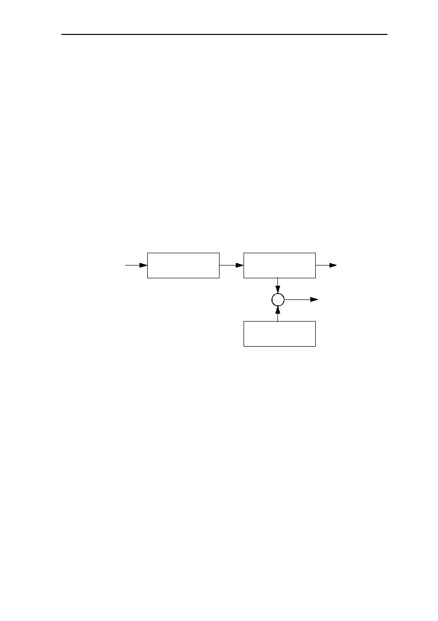
TIMER 5-1
5. Timer and CPU Clock Modes
5.1 Overview
The on-chip timer is controlled via three registers:
Timer prescaler register TPR G21
Timer register TR G23
Timer compare register TCR G22
G21..G23 can be addressed only via the high global flag H by a MOV or MOVI instruction.
The content of G21 (timer prescaler register) cannot be read.
The write-only TPR sets a carry flag C (overflow) when the value of the counter in TPR
equals to the content of TPR, and transfers carry flag C to the TR. When the TPR transfers
carry flag to the TR, TR increments by one on modulo 2
32
. Timer clock frequency is
determined by the content of TPR.
When the TR higers than or equals to the TCR, the timer interrupt is generated.
TR
TCR
x
Timer Interrupt
TPR
Processor Clock
Frequency
Timer Clock
Frequency
carry
compare
Fig. 5.1 The block diagram of on-chip timer.
5.1.1 Timer Prescaler Register TPR
Global register G21 is the write-only Timer Prescaler Register TPR. The TPR adapts the
timer clock to different processor clock frequencies and controls the PLL clock output.
Bits 26 and 27 select the processor clock. Bits 23..16 determine the basic time unit
frequency of timer clock := frequency of processor clock divided by (n+2)
n
is the value to be loaded into the TPR at the bit positions 23..16, it is calculated according
to the formula:
n = (time unit
frequency of processor clock) - 2
Bit 31 determines the effect of a write to TPR. If bit 31 is 0, a write to TPR takes
effect immediately, the processor clock divider is changed and the timer prescaler
divider is reloaded. If bit 31 is 1, the processor clock divider and timer prescaler
divider update is delayed until the current basic time unit ends. At the end of the
current time unit, the processor clock divider and the timer prescaler divider are
updated with the new values. This allows keeping absolute timing even when the
5-2 CHAPTER 5
processor clock is changed by simultaneously changing the processor clock
divider and the timer prescaler divider.
The TPR is initialized to bit 27=1, bits 26 and 23..16=0 on reset (from the
RTESET# pin or by a clock-Down reset), i.e. the processor starts with CPU clock =
XTAL1 clock, the prescaler divides by 2. During a Watchdog (IO3 Timer) Reset,
the TPR is preserved, This allows the use of the Watchdog as a controlled time-
out without losing the time base.
Bits 30..28, 25..24 and 15..0 are reserved and must be zero on a move to TPR.
Bits
Name
Description
31
LoadEnable
1 = TPR update is de3layed until current prescaler time unit ends
0 = TPR update is performed immediately
30..28
Reserved
27..26 ClockDivider
CPU Clock Divider Control
11 = CPU clock = XTAL1 clock / 2
10 = CPU clock = XTAL1 clock
01 = CPU clock = XTAL1 clock * 2
00 = CPU clock = XTAL1 clock * 4
25..24
Reserved
23..16 TimerPrescaler
Timer Prescaler Division factor n
Range n = 0..255, Timer Prescaler divides by n+2
15..0
Reserved
Table 5.1: Memory Address Spaces
5.1.2 Timer Register TR
The TR is a 32-bit register that is incremented by one on each time unit modulo 2
32
. Its
content can be used as the lower word of a double-word integer, representing the time
inclusive date.
The TPR and the TR should be set only once on system initialization, whereby the
following instruction sequence must be observed strictly (interrupts must be locked out):
:
:
FETCH 4
ORI SR, $20 ; set H-flag
MOV TPR, Lx ; load prescaler register from local register x
ORI SR, $20 ; set H-flag
MOV TR, Ly ; load timer register from local register y
:
:
Note: The Fetch instruction is necessary to prevent insertion of idle cycles during the
prescripted instruction sequence.

TIMER 5-3
5.1.3 Timer Compare Register TCR
The content of the TCR is compared continuously with the content of the timer register TR.
An unsigned modulo comparison is performed according to:
result(31..0) := TR(31..0) - TCR(31..0)
On
result(31)
= 0, the TR is higher than or equal to the TCR.
When the timer interrupt is enabled (FCR(23) = 0) and the value in the TR is higher than
or equal to the value in the TCR, a timer interrupt is generated. This interrupt is cleared by
loading the TCR with a value higher than the current content of the TR.
Timer interrupts can be masked out by FCR(23) = 1; FCR(23) is set to one on Reset. The
timer interrupt disable bit FCR(23) does not affect the timer and compare function.
A delay time in the TCR is calculated according to the formula:
TCR := current content of TR + number of delay time units
The maximum
number of delay time units
allowed for this calculation is 2
31
-1.
For example:
TR(31..0) =
hex
FFFF FF00
delay time units (= 1000) =
hex
0000 03E8
TCR(31..0) =
hex
0000 02E8
Since the modulo comparison is an unsigned operation, only unsigned arithmetic must be
used for calculations with timer and timer compare values. Do not use the N or C flag to
test for the result of the comparison TR - TCR, use only result bit 31!
5.1.4 Power-Down Mode
When the power-down mode is entered, the execution pipeline of the processor is halted.
Only the logic for the timer, IO3 control modes, interrupt and refresh is being clocked, all
other clocks are disabled. The processor is temporarily activated for refresh and bus
arbitration cycles, no instructions are executed during these temporary clock cycles. The
processor resumes execution by any interrupt or on a reset.
Power-down mode can be entered by executing an I/O write instruction with address bits
A(27) and A(25..23) set to one and A(22) set to zero.
When power-down mode is entered via the I/O write instruction, the power-down mode
takes effect at the time when the I/O access is performed. Until this time, instruction
execution continues. To ensure that the power-down mode takes effect, the power-down
I/O access can be followed by a dummy load accesses (I/O or memory). A following
dependent instruction then waits until both I/O accesses are performed. Thus, instructions
following the MOV instruction are not executed until wakeup. Note that even though the
power-down request is an internal operation of the processor, bus grant must be given so
that the power-down I/O access can be performed.

5-4 CHAPTER 5
Power-down mode can be set by a program sequence as in the following example:
PowerDownIO EQU 1 << 27 | %1110 << 22 ; Bits 27, 25..23, 22
...
STW.IOA 0, 0, PowerDownIO ; set power-down mode
LDW.IOA 0, L4, PowerDownIO ; wait until power-down
MOV L4, L4 ; I/O is executed
... ; execution continues
; here after wakeup
5.1.5 Additional Power Saving
The CPU clock divider control can be used for example to switch the CPU to a slow clock
during power-down for additional power savings. In the following example, the XTAL1
clock is 20 MHz, the CPU runs normally at 80 MHz and is switched back to 10 MHz
during power-down. The timer prescaler setting is changed so that a time unit of 1 µs is
kept through the power-down sequence. Using the "delayed TPR update" feature, the 1 µs
absolute time is maintained even for the time units where the TPR setting changes.
Interrupts are locked out during power-down using the L bit in SR. This is done so that the
TPR setting can be changed back to fast clock and corresponding prescaler setting after
wakeup from power-down before the interrupt handler is called. The interrupt occurs at the
time the lock bit L in SR is cleared. The power-down is initiated by executing the power-
down I/O access. The power-down is guaranteed to be effective before the next (dummy)
I/O load access is done, thus the following MOV instruction is not executed until wakeup.
The instructions to restore the CPU clock speed and the prescaler setting can thus be
placed after the dummy load and MOV instructions.
TPR_fast EQU %00 << 26 | 78 << 16 ; fast TPR, divide by 80
TPR_slow EQU %11 << 26 | 8 << 16 ; slow TPR, divide by 10
DelayTPRUpd EQU 1 << 31 ; delayed TPR update
L_Bit EQU 1 << 15 ; Interrupt Lock in SR
H_Bit EQU 1 << 5 ; High-Global Bit in SR
PowerDownIO EQU 1 << 27 | %1110 << 22 ; Power-Down I/O address
...
MOVI L5, TPR_slow ; TPR for power-down
MOVI L6, TPR_fast ; TPR after power-down
ORI L5, DelayTPRUpd ; set delayed TPR update
ORI L6, DelayTPRUpd ; set delayed TPR update
ORI SR, L_Bit | H_Bit ; set Interrupt Lock
MOV TPR, L5 ; set slow clock
STW.IOA 0, 0, PowerDownIO ; set power-down mode
LDW.IOA 0, L4, PowerDownIO ; dummy load
MOV L4, L4 ; wait till done
; next instruction is
; executed after wakeup
ORI SR, H_Bit
MOV TPR, L6 ; restore fast clock
ANDNI SR, L_Bit ; allow interrupt now
... ; continue here after
; interrupt routine has
; been executed

TIMER 5-5
5.1.6 Sleep Mode
To further reduce power dissipation, the processor can be set into sleep mode. In this case,
the clock of the processor is completely switched off. When a quartz crystal is used for
processor clock generation, it is also switched off. An external reset signal or an interrupt
awakes the processor from sleep mode and the processor continues with the standard reset
procedure. Bit 10 in ISR indicates that the reset was caused by a wakeup from sleep mode.
The sleep mode can be entered by an I/O write instruction with address bits A(27) and
A(25..22) set to one. Note that any content of the internal RAM and the external DRAM as
well as the timer count will be lost during sleep mode. The sleep mode takes effect when
the I/O access is performed. After this, the processor behaves as in reset, i.e. the bus
request is deactivated until wakeup by an interrupt or reset. On wakeup by an interrupt, the
FCR setting is preserved through the reset sequence. As with the power-down I/O access, a
dummy load access could be placed after the sleep mode I/O access to ensure that the sleep
mode takes effect. Since the processor continues with a reset at wakeup from sleep mode,
an empty loop can be used as well to wait until the sleep mode I/O access has taken effect.
Note that even though sleep mode is an internal operation of the processor, bus grant must
be given so that the sleep mode set I/O access can be performed.
An interrupt signal awaking the processor from sleep mode must stay active at least until
the processor has begun executing its reset sequence. This latency time includes the startup
time of the crystal oscillator and of the PLL circuit. If the interrupt goes inactive before
this latency time has elapsed, the processor may fall back into sleep mode. In order to have
the effect of causing a processor interrupt, the interrupt signal should stay active until it is
acknowledged by the interrupt handler.
The sleep mode can be set by a program sequence as in the following example:
SleepModeIO EQU 1 << 27 | %1111 << 22 ; Bits 27, 25..22
...
STW.IOA 0, 0, SleepModeIO ; set sleep mode
SleepWait: BR SleepWait ; wait until sleep
; mode I/O is executed

BUS INTERFACE 6-7
6. Bus Interface
6.1 Bus Control General
The processor provides on-chip all functions for controlling memory and peripheral
devices, the including RAS-CAS multiplexing, DRAM refresh and parity generation and
checking. The number of bus cycles used for a memory or I/O access is also defined by the
processor; thus, no external bus controllers are required. All memory and peripheral
devices can be connected directly, pin by pin, without any glue logic.
The memory address space is divided into five partitions as follows:
Address (hex)
Address Space
Memory Type
0000 0000..3FFF FFFF Address Space MEM0
ROM, SRAM, DRAM
4000 0000..7FFF FFFF Address Space MEM1
ROM, SRAM
8000 0000..BFFF FFFF Address Space MEM2
ROM, SRAM
C000 0000..DFFF FFFF Address Space IRAM
Internal RAM (IRAM)
E000 0000..FFFF FFFF Address Space MEM3
ROM, SRAM
Table 6.1: Memory Address Spaces
The bus timing, refresh control and parity error disable for memory access is defined in the
bus control register BCR. The bus timing for I/O access is defined by address bits in the
I/O address.
On a memory or I/O access, the address bus signals are valid through the whole access. On
a memory access, the chip select signal for the selected memory area MEM0..MEM3 is
switched to low (active low) through the whole access. On a write access to memory or I/O,
the data bus and the parity signals are also activated and the write enable signal WE# is
switched to low through the whole access.
A bus wait cycle is inserted automatically to guarantee a minimum of one idle cycle
between the end of an output enable signal (OE#, IORD#, CASx# at read) and the
beginning of a subsequent write access. After a DRAM read access with an access time > 2
cycles, an additional bus wait cycle is inserted.

6-8 CHAPTER 6
6.1.1 Boot Width Selection
The processor provides two pins (BOOTW and BOOTB) for selecting the data bus width
for memory area MEM3 (boot memory area). Table 6.2 shows the encoding for selecting
the desired data bus width. The pin state is sampled during reset.
BOOTW
BOOTB
Data Bus Width
Don' t care
HIGH
8-bit
LOW
LOW
16-bit
HIGH
LOW
32-bit
Table 6.2: Data bus width encoding for memory area MEM3
The pins used for BOOTB and BOOTW were used as VCC pins at the GMS30C2232 and
GMS30C2216.
Thus, if the GMS30C2232 is used as a direct replacement for the GMS30C2132, the
GMS30C2232 defaults to 8-bit MEM3 width as the GMS30C2132 did.
BOOTW is tied low internally for the GMS30C2216 processor, the BOOTB pin can then
be used to select between 8-bit and 16-bit MEM3 bus width.
6.1.2 SRAM and ROM Bus Access
On a one-cycle SRAM or EPROM read access, the output enable signal OE# is switched to
low during the second half of the access cycle; on a multi-cycle read access, OE# is
switched to low after the first access cycle and remains low through the rest of the
specified access cycles. On a SRAM write access, the write enable signals WE0#..WE3#
corresponding to the bytes to be written are switched to low analogous to the OE# signal
for single and multiple access cycles.
For memory area MEM2, an address setup cycle preceding the access cycles can be
specified. For MEM0..MEM3, bus hold cycles can be specified. Bus hold cycles are
additional cycles succeeding the access cycles where neither OE# nor WE0#..WE3# is low
but all other bus signals are asserted. The bus hold cycles can be specified to be skipped or
enforced. (see section
6.4.7. MEMx Bus Hold Break
).
BUS INTERFACE 6-9
6.1.3 DRAM Bus Access
A DRAM access to the same DRAM page as addressed by the previous DRAM access is
executed as fast page mode access. See bus control register BCR(17..16) for the access
time and low-cycles of the CASx# signals. CAS0#..CAS3# signals enable the
corresponding memory bytes 0..3.
A RAS access occurs when the DRAM page is different from the previously accessed
DRAM page. The RAS# signal is switched to high for the number of specified precharge
cycles. The high-order row address bits are multiplexed to the bit positions of the low-
order column address bits according to the specified page size after the first bus cycle until
the end of the specified RAS-to-CAS delay cycles. After the RAS-to-CAS delay cycles,
the column address bits are available on the low-order bit positions and the CAS access
cycle begins.
The row address bits are available at the high-order bit positions for the whole DRAM
access. After a DRAM access, the addressed DRAM page is being available for fast page
mode accesses to the same page until either a new DRAM page is addressed, the processor
is released to another bus master for DMA or a DRAM refresh takes place.
Note: The multiplexed row address bits are not in any specific order.
DRAM Read and Write Cycle
(1) Write Cycle
Active word line
TR: ON
Load stored data to
bit line
Data write
(2) Read Cycle
Apply V
DD
/2 to bit line
Active word line
Read
data
stored in capacitor
(3) Refresh (CAS before RAS)
CAS before RAS signal
Enter refresh mode
Store
original data to sense amplifier
Active word line
Refresh (data write)
Word Line (Row Address Line)
Pass
Transister
Capacitor
Bit Line (Column Address Line)

6-10 CHAPTER 6
6.1.3.1 DRAM Row Address Bits Multiplexing
Table 8.3 shows the DRAM row address bits multiplexing. The page size code is specified
in the Bus Control Register BCR. The gray fields denote the multiplexed DRAM row
address bits. The white fields denote the DRAM row address bits that are not
multiplexed.
Address Bus bits
31..16
15 14 13 12 11 10 9 8 7 6 5 4 3 2 1 0
Page Size
Code
DRAM Row Address Bits
0 (000
2
)
31..16
29 27 25 23 21 19 17 28 26 24 22 20 18 16
£ -
£ -
1 (001
2
)
31..16
15 27 25 23 21 19 17 16 26 24 22 20 18 16 28 29
2 (010
2
)
31..16
15 14 25 23 21 19 17 15 14 24 22 20 18 16 26 27
3 (011
2
)
31..16
15 14 13 23 21 19 17 15 14 13 22 20 18 16 24 25
4 (100
2
)
31..16
15 14 13 12 21 19 17 15 14 13 12 20 18 16 22 23
5 (101
2
)
31..16
15 14 13 12 11 19 17 15 14 13 12 11 18 16 20 21
6 (110
2
)
31..16
15 14 13 12 11 10 17 15 14 13 12 11 10 16 18 19
7 (111
2
)
31..16
15 14 13 12 11 10 9 16 14 13 12 11 10 9 16 17
Table 6.3: DRAM Row Address Bits Multiplexing
Note: DRAM can only be connected to memory area MEM0. The address bit A0 of the
address bus is not used in case of a 16-bit bus size for memory area MEM0. The address
bits A1 and A0 of the address bus are not used in case of a 32-bit bus size for memory area
MEM0. In case of page size code 0, only a 32-bit bus size for memory area MEM0 can be
used. Memory area MEM0 is only selected, if address bits A31 and A30 of a memory
address are zero.

BUS INTERFACE 6-11
6.2 I/O Bus Access
The bus timing for an I/O access is specified by bits 11..3 of the I/O address.
On an I/O access, the I/O read strobe IORD# or the I/O write strobe IOWR# is switched
low for a read or write access respectively after the first access cycle and remains low for
the rest of the specified access cycles. The beginning of the IORD# or IOWR# signal can
be delayed by more than one cycle by specifying additional address setup cycles preceding
the access cycles. The beginning of the next bus access can be delayed by specifying bus
hold cycles succeeding the access cycles. Bus hold cycles are required by many I/O
devices due to the time required to switch from driving the data bus to three states.
Bit 11 of the I/O address enables a wait-pin controlled I/O access. The INT3/WAIT input
of the processor is sampled after the first three access cycles of the specified I/O access
time. The I/O access will be extended by inserting further access cycles as long as the sig-
nal at the WAIT input is asserted. When the WAIT signal becomes deasserted, the access
will be terminated. Note that there is latency of about 2..3 processor cycles until a signal
change at the WAIT input becomes effective. The polarity of the WAIT signal can be
programmed via bit 26 of the
Function Control Register FC
R. When FCR(26) is set to 1
(default after reset), the WAIT signal is high asserted; when FCR(26) is set to 0, the WAIT
signal is low asserted. A minimum of four I/O access cycles must be specified when the
I/O wait mode is being enabled.
When an I/O device requires R/W# direction and data strobe control, IORD# can be
specified (by address bit 10 = 1) as data strobe. WE# is then used as R/W# signal.
......
Reserved
11
10
9
8
7
6
5
4
3
2
1
0
I/O Address
Wait Enable
Peri. Device Control Mode
0=IORD#/IOWR#
1=R/W#/DATA strobe control
Address Set-Up Time
00=0 Cycle
01=2 Cycle
10=4 Cycle
11=8 Cycle
Access Time
000=2 Cycle
001=4 Cycle
010=6 Cycle
011=8 Cycle
100=10 Cycle
101=12 Cycle
110=14 Cycle
111=16 Cycle
Bus Hold Time after Read/Write Access
00 = none
01 = 2 Cycle
10 = 4 Cycle
11 = 6 Cycle
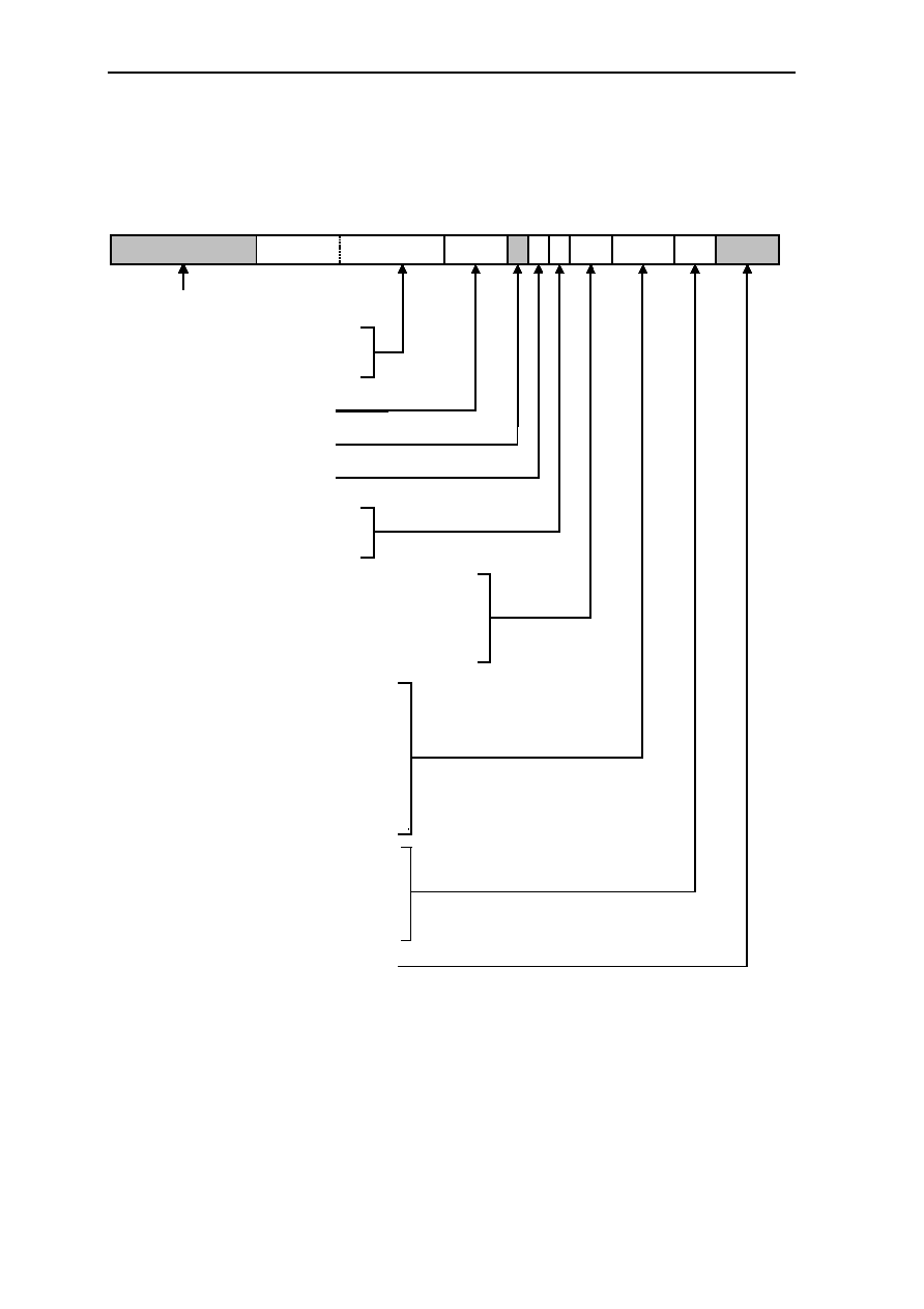
6-12 CHAPTER 6
6.2.1 I/O Bus Control
With I/O addresses, address setup, access and bus hold time can be specified by bits in the
I/O address as follows:
0
2
3
4
5
7
8
9
10
Reserved (must be 0)
Address Setup Time before Read or Write Access
00 = 0 cycles
01 = 2 cycles
10 = 4 cycles
11 = 6 cycles
Access Time for Read or Write Access
000 = 2 cycles
001 = 4 cycles
010 = 6 cycles
011 = 8 cycles
100 = 10 cycles
101 = 12 cycles
110 = 14 cycles
111 = 16 cycles
Bus Hold Time after Read or Write Access
00 = 0 cycles
01 = 2 cycles
10 = 4 cycles
11 = 6 cycles
Reserved for System Peripheral
11
Peripheral Device Control Mode
0 = IORD# / IOWR# Strobe Control
1 = R/W# / Data Strobe Control
21
25
I/O Address and/or I/O Chip Select
GMS30C2216: 6 Bits
GMS30C2232: 10 Bits
12
13
Wait Enable
Reserved for Internal Use (must be 0)
I/O Register Address
15
Figure 6.1: I/O Bus Control
Reserved bits must always be supplied as zero when specifying an I/O address in a
program.

BUS INTERFACE 6-13
6.3 Bus Control Register BCR
Global register G20 is the write-only bus control register BCR. The BCR defines the
parameters (bus timing, refresh control, page fault and parity error disable) for accessing
external memory located in address spaces MEM0..MEM3.
All bits of the BCR are set to one on Reset. They are intended to be initialized according to
the hardware environment.
Bits
Name
Description
31..28 Mem3Access
Access time for address space MEM3
1111 = 16 clock cycles
1110 = 15 clock cycles
1101 = 14 clock cycles
1100 = 13 clock cycles
1011 = 12 clock cycles
1010 = 11 clock cycles
1001 = 10 clock cycles
1000 = 9 clock cycles
0111 = 8 clock cycles
0110 = 7 clock cycles
0101 = 6 clock cycles
0100 = 5 clock cycles
0011 = 4 clock cycles
0010 = 3 clock cycles
0001 = 2 clock cycles
0000 = 1 clock cycle
27..24 Mem2Access
Access time for address space MEM2
1111 = 16 clock cycles
1110 = 15 clock cycles
1101 = 14 clock cycles
1100 = 13 clock cycles
1011 = 12 clock cycles
1010 = 11 clock cycles
1001 = 10 clock cycles
1000 = 9 clock cycles
0111 = 8 clock cycles
0110 = 7 clock cycles
0101 = 6 clock cycles
0100 = 5 clock cycles
0011 = 4 clock cycles
0010 = 3 clock cycles
0001 = 2 clock cycles
0000 = 1 clock cycle
23
Mem1Hold
Bus hold time code for address space MEM1
When BCR(22) = 1:
1 = 2 clock cycles
0 = 1 clock cycle
When BCR(22) = 0
1 = 1 clock cycle
0 = 0 clock cycles

6-14 CHAPTER 6
Bits
Name
Description
22..20 Mem1Access
Access time for address space MEM1
111 = 8 clock cycles
110 = 7 clock cycles
101 = 6 clock cycles
100 = 5 clock cycles
011 = 4 clock cycles
010 = 3 clock cycles
001 = 2 clock cycles
000 = 1 clock cycle
MEM0 = Non-DRAM (MCR(21) = 1):
19..16 Mem1Access
Access time for address space MEM0
1111 = 16 clock cycles
1110 = 15 clock cycles
1101 = 14 clock cycles
1100 = 13 clock cycles
1011 = 12 clock cycles
1010 = 11 clock cycles
1001 = 10 clock cycles
1000 = 9 clock cycles
0111 = 8 clock cycles
0110 = 7 clock cycles
0101 = 6 clock cycles
0100 = 5 clock cycles
0011 = 4 clock cycles
0010 = 3 clock cycles
0001 = 2 clock cycles
0000 = 1 clock cycle
14
Mem0Setup
Address setup time for address space MEM0
11 = 3 clock cycles
10 = 2 clock cycles
01 = 1 clock cycle
00 = 0 clock cycles
13..11 Mem0Hold
Address setup time for address apace MEM0
111 = 7 clock cycles
110 = 6 clock cycles
101 = 5 clock cycles
100 = 4 clock cycles
011 = 3 clock cycles
010 = 2 clock cycles
001 = 1 clock cycles
000 = 0 clock cycles
MEM0 = Non-DRAM (MCR(21) = 0):
19..18 RasPrecharge
RAS precharge time for address space MEM0
when MCR(8)=0 when MCR(8)=1
11 = 4 clock cycles 6 clock cycles
10 = 3 clock cycles 5 clock cycles
01 = 2 clock cycles 4 clock cycles
00 = 1 clock cycle 3 clock cycles

BUS INTERFACE 6-15
Bits
Name
Description
17..16 CASAccess
CAS access time for address space MEM0
when MCR(8)=0 when MCR(8)=1
11 = 4 clock cycles 6 clock cycles
10 = 3 clock cycles 5 clock cycles
01 = 2 clock cycles 4 clock cycles
00 = 1 clock cycle 3 clock cycles
15..14 RasToCas
Ras to CAS delay time
11 = 4 clock cycles
10 = 3 clock cycles
01 = 2 clock cycles
00 = 1 clock cycle
13..11 RefreshSelect
Refresh rate select (CAS before RAS refresh)
111 = Refresh disabled
110 = Refresh every 4 prescaler time units
101 = Refresh every 8 prescaler time units
100 = Refresh every 16 prescaler time units
011 = Refresh every 32 prescaler time units
010 = Refresh every 64 prescaler time units
001 = Refresh every 128 prescaler time units
000 = Refresh every 256 prescaler time units
10..8
Mem3Hold
Bus hold time code for address space MEM3
111 = 7 clock cycles
110 = 6 clock cycles
101 = 5 clock cycles
100 = 4 clock cycles
011 = 3 clock cycles
010 = 2 clock cycles
001 = 1 clock cycle
000 = 0 clock cycles
7
Mem3Setup
Address setup time for address space MEM3
1 = 1 clock cycle
0 = 0 clock cycles
6..4
PageSizeCode
Page size code
3
Mem2Setup
Address setup time for address space MEM2
1 = 1 clock cycle
0 = 0 clock cycles
2..0
Mem2Hold
Bus hold time code for address space MEM2
111 = 7 clock cycles
110 = 6 clock cycles
101 = 5 clock cycles
100 = 4 clock cycles
011 = 3 clock cycles
010 = 2 clock cycles
001 = 1 clock cycle
000 = 0 clock cycles
Table 6.4: Bus Control Register BCR
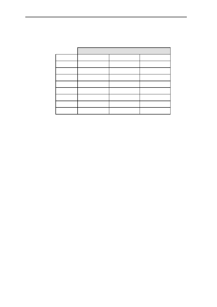
6-16 CHAPTER 6
The DRAM type used and the physical page size of the DRAM are specified by bits 6..4,
in the BCR. Table 8.5 shows the encoding of BCR(6..4) and the associated column address
ranges for memory areas with bus sizes of 32, 16 and 8 bits.
Columns Address Range
BCR(6..4) 32-bit Bus Size 16-bit Bus Size 8-bit Bus Size
000
A15..A2
A15..A1
A15..A0
001
A14..A2
A14..A1
A14..A0
010
A13..A2
A13..A1
A13..A0
011
A12..A2
A12..A1
A12..A0
100
A11..A2
A11..A1
A11..A0
101
A10..A2
A10..A1
A10..A0
110
A9..A2
A9..A1
A9..A0
111
A8..A2
A8..A1
A8..A0
Table 6.5: Column Address Ranges

BUS INTERFACE 6-17
6.4 Memory Control Register MCR
Global register G27 is the write-only memory control register MCR. The MCR controls
additional parameters for the external memory, the internal memory refresh rate, the
mapping of the entry table and the processor power management. All bits of the MCR are
set to one on Reset except for the MEM3BusSize bits that are initialized from the BOOTW
and BOOTB pads. The MCR bits must be initialized according to the hard ware
environment and the desired function.
Bits
Name
Description
31
MEM3ParityDisable Parity check disable for address space MEM3
1 = disabled
0 = enabled
30
MEM2ParityDisable Parity check disable for address space MEM2
1 = disabled
0 = enabled
29
MEM1ParityDisable Parity check disable for address space MEM1
1 = disabled
0 = enabled
28
MEM0ParityDisable Parity check disable for address space MEM0
1 = disabled
0 = enabled
27
Reserved
26
MEM2WaitDisable Wait signal disable for address space MEM2
1 = disabled
0 = enabled
25
Reserved
24
Reserved
23
MEM2ByteMode
Byte write access mode for address space MEM2
1 = WE0# .. WE3# act as byte write strobe
0 = WE0# .. WE3# act as byte enable signal
22
Reserved for internal use
21
MEM0MemoryType 1 = Non-DRAM
0 = DRAM
20
IRAMRefreshTest
1 = Normal Mode
0 = Test Mode
19
MEM1ByteMode
Byte write access mode for address space MEM1
1 = WE0# .. WE3# act as byte write strobe
0 = WE0# .. WE3# act as byte enable signal
18..16 IRAMRefreshRate
111 = Disabled
110 = Refresh every 2 prescaler time units (recommended)
101 = Refresh every 4 prescaler time units
100 = Refresh every 8 prescaler time units
011 = Refresh every 16 prescaler time units
010 = Refresh every 32 prescaler time units
001 = Refresh every 64 prescaler time units
000 = Refresh every 128 prescaler time units

6-18 CHAPTER 6
Bits
Name
Description
MEM0 = Non-DRAM (MCR(21) = 1):
15
MEM0ByteMode
Byte write access mode for address space MEM0
1 = WE0# .. WE3# act as byte write strobe
0 = WE0# .. WE3# act as byte enable signal
MEM0 = Non-DRAM (MCR(21) = 0):
15
DRAMType
1 = Fast Page Mode DRAMs
0 = EDO DRAMs
14..12 EntryTableMap
111 = MEM3
110 = reserved
101 = reserved
100 = reserved
011 = Internal RAM (IRAM)
010 = MEM2
001 = MEM1
000 = MEM0
11
MEM3BusHoldBrea
k
1 = Break Disabled
0 = Break Enabled
10
MEM2BusHoldBrea
k
1 = Break Disabled
0 = Break Enabled
9
MEM1BusHoldBrea
k
1 = Break Disabled
0 = Break Enabled
MEM0 = Non-DRAM (MCR(21) = 1):
8
MEM0BusHoldBrea
k
1 = Break Disabled
0 = Break Enabled
MEM0 = Non-DRAM (MCR(21) = 0):
8
DRAMBusHold
1 = Break Enabled, Bus Hold time 1 cycle
0 = Break Enabled, Bus Hold time 0 cycle
7..6
MEM3BusSize
11 = 8 bit
10 = 16 bit
01 = reserved
00 = 32 bit
5..4
MEM2BusSize
11 = 8 bit
10 = 16 bit
01 = reserved
00 = 32 bit
3..2
MEM1BusSize
11 = 8 bit
10 = 16 bit
01 = reserved
00 = 32 bit
1..0
MEM0BusSize
11 = 8 bit
10 = 16 bit
01 = reserved
00 = 32 bit
Table 6.6: Memory Control Register MC

BUS INTERFACE 6-19
6.4.1 MEMx Parity Disable
Bits 31..28 of the MCR control parity generation and parity check for each memory area.
The default setting is parity check disables. The appropriate MCR bit must be cleared to
enable the parity check for that memory area.
6.4.2 MEMx Wait Disable
Bit 26 of the MCR controls the wait pin function for the memory area MEM2. The default
setting is wait function disabled. The MCR bit must be cleared to enable the wait function
for the MEM2 memory area. When this function is enabled, the INT2/WAIT input of the
processor is used as wait pin. Any MEM2 memory access remains active as long as the
signal at the WAIT input is asserted (the WAIT input is sampled after the first three access
cycles of the memory access). The access will be terminated after the WAIT input becomes
disserted. Whether the input is low-asserted or high-asserted can be programmed via bit 26
of the Function Control Register FCR. A minimum access time of four cycles must be
specified for a memory area with the wait function enabled.
If the INT3/WAIT input is used as wait pin, bit 30 of the FCR (INT3Mask) should be set to
1 so that no interrupts are generated on the assertion of WAIT.
6.4.3 MEMx Byte Mode
Bit 23, 19, and 15 of the MCR control the byte write access mode for memory areas
MEM2, MEM1, and MEM0, respectively. The default setting is byte-write-strobe,
meaning that the signals WE0#..WE3# are used as write strobe signals for writing the
appropriate data byte to the external memory. When the MCR bit is cleared, the signals
WE0#..WE3# act as a byte enable signal and the general WE# signal must be used for
writing the data to the memory.
Note: Most SRAM chips with 16-bit or 32-bit wide data interface require a single write-
enable signal and dedicated enable signals for each byte. The setting MEMxByteMode = 0
is intended specifically for those types of memories.
6.4.4 Power Down
Bit 22 of the MCR controls the power-down mode. The default setting is
processor active
.
To switch the processor to power-down mode MCR(22) must be cleared. The switch to
power-down is initiated by a transition from MCR(22) = 1 to MCR(22) = 0; thus,
MCR(22) must be restored to one for at least one cycle before a new switch to power-down
mode can occur.
In power-down mode, only the logic for the timer, IO3Control modes, interrupt and refresh
is being clocked, all other clocks are disabled. The switch to power-down mode is delayed
until the memory pipeline is empty. The processor is activated temporarily for refresh and
bus arbitration cycles and is switched back to
processor active
by any interrupt or on Reset.
Note that MCR(22) is not switched back to one by an interrupt.
6.4.5 IRAM Refresh Test
Bit 20 of the MCR specifies the internal RAM (IRAM) refresh test. The default setting is
normal mode, MCR(20) = 0 specifies refresh test mode.

6-20 CHAPTER 6
6.4.6 IRAM Refresh Rate
Bits 18..16 of the MCR specify the IRAM refresh rate in number (4..256) of prescaler
time units. The default setting is disabled. Recommended refresh rate for normal IRAM
usage is every 2 prescaler time units.
6.4.7 DRAM Type
When the MEM0 memory type is set to DRAM (MCR(21)=0), bit 15 of the MCR acts as
control bit for selecting the DRAM type. The default setting is Fast-Page-Mode DRAM.
To support EDO DRAMs, MCR(15) must be cleared.
When the DRAM type indicates Fast-Page-Mode DRAMs, the OE# signal of the processor
is left disserted during DRAM accesses. The OE# pin of the DRAMs must then be tied low
for correct DRAM operation.
When the DRAM type indicates EDO DRAMs, OE# must be connected to the DRAMs
and is asserted on DRAM read accesses. OE# stays active for one half clock cycle past the
end of the CAS# signals, the read data is sampled at the end of OE#. Thus, the processor
can take advantage of the EDO fracture.
6.4.8 Entry Table Map
Bits 14..12 of the MCR map the entry table to one of the memory areas MEM0..MEM3 or
to the IRAM. With a mapping to MEM3 (default setting), the entry table is mapped to the
end of MEM3, with all other settings, the entry table is mapped to the beginning of the
specified memory area.
6.4.9 MEMx Bus Hold Break
Bits 11..8 specify a memory bus hold break for MEM3..MEM0 respectively. The default
setting is
disabled
. With
enabled
, bus hold cycles are skipped when the next memory access
addresses the same memory area. Regularly, the bus hold break should be
enabled
; it must
only be left
disabled
to accommodate (rare) SRAMs or ROMs which need all specified
cycles before a new access can be started (e.g. for charge restore).
If the MEM0 memory type is DRAM, bit 8 changes the RasPrecharge and CASAccess
cycle counts specified in BCR, and specifies a bus hold time of 0 or 1 cycle. Bus hold
break for DRAM is always enabled.
6.4.10 MEMx Bus Size
Bits 7..0 specify the bus size for each of the four memory areas

BUS INTERFACE 6-21
6.5 Input Status Register ISR
Global register G25 is the read-only input status register ISR. The ISR reflects the input
levels at the pins IO1..IO3 as well as the input levels at the four interrupt pins INT1..INT4
and contains the EventFlag, the EqualFlag, the WatchdogFlag and the ClockOnFlag. Re-
served bits are read as.
The input levels are not affected by the polarity bits in the Function Control Register FCR,
they reflect always the true signal level at the corresponding pins with a latency of 2..3
cycles, a 1 signals high level.
Bits
Name
Description
31..11
Reserved
10
ClockOnFlag
Determines the source of the last reset event
1 = Last reset caused by a clock-down command
0 = Last reset caused by RESET# signal or watchdog timer
9
WatchdogFlag
Determines the source of the last reset event
1 = Last reset caused by watchdog timer (IO3 timer)
0 = Last reset caused by RESET# signal or clock-down
command
8
EventFlag
Set to 1 in IO3Timing Mode when IO3Level is equal to
IO3Polarity
Cleared to 0 by FCR(13) = 1 or write to the WCR
7
EqualFlag
Set to 1 in IO3Timing or IO3TimerInterrupt Mode when
WCR(15..0) = TR(15..0)
Cleared to 0 by FCR(13) = 1 or write to the WCR
6
IO3Level
Reflects the signal level at the IO3 Pin
1 = High Level
0 = Low Level
5
IO2Level
Reflects the signal level at the IO2 Pin
1 = High Level
0 = Low Level
4
IO1Level
Reflects the signal level at the IO1 Pin
1 = High Level
0 = Low Level
3
Int4Level
Reflects the signal level of interrupt input INT4
1 = High Level
0 = Low Level
2
Int3Level
Reflects the signal level of interrupt input INT3
1 = High Level
0 = Low Level
1
Int2Level
Reflects the signal level of interrupt input INT2
1 = High Level
0 = Low Level
0
Int1Level
Reflects the signal level of interrupt input INT1
1 = High Level
0 = Low Level
Table 6.7: Input Status Register ISR

6-22 CHAPTER 6
6.6 Function Control Register FCR
Global register G26 is the write-only function control register FCR. The FCR controls the
polarity and function of the I/O pins IO1..IO3 and the interrupt pins INT1..INT4, the timer
interrupt mask and priority, the bus lock, the CLKOUT pin and the Extended Overflow
exception. All bits of the FCR are set to one on Reset exception (from the RESET# pin or
as a result of a watchdog overrun). They must be initialized according to the hardware
environment and the desired function. The reserved bits must not be changed when the
FCR is updated.
The FCR is preserved on a clock-down reset in order to have the correct interrupt mask and
polarity for the wakeup from clock-down.
Each of the four interrupt pins INT1..INT4 can cause a processor interrupt when the
corresponding interrupt mask bit is cleared. The corresponding polarity bit determines
whether the signal at the interrupt pin must be low (polarity bit = 0) or high (polarity
bit = 1) to cause an interrupt. Additionally, the internal timer interrupt can be enabled or
disabled separately.
Each of the I/O pins IO1..IO3 can be either used as input or interrupt signal (IOxDirection
= 1) or as output (IOxDirection = 0). The CLKOUT pin of the processor can be pro-
grammed to provide a static output level of either high or low, or it can be configured to
provide the processor's internal clock signal undivided or divided by two or four.
Bits
Name
Description
31
INT4Mask
1 = Interrupt INT4 Disabled
0 = Interrupt INT4 Enabled
30
INT3Mask
1 = Interrupt INT3 Disabled
0 = Interrupt INT3 Enabled
29
INT2Mask
1 = Interrupt INT2 Disabled
0 = Interrupt INT2 Enabled
28
INT1Mask
1 = Interrupt INT1 Disabled
0 = Interrupt INT1 Enabled
27
INT4Polarity
1 = Non-Inverted (Interrupt on High Level)
0 = Inverted (Interrupt on Low Level)
26
INT3Polarity
1 = Non-Inverted (Interrupt on High Level)
0 = Inverted (Interrupt on Low Level)
25
INT2Polarity
1 = Non-Inverted (Interrupt on High Level)
0 = Inverted (Interrupt on Low Level)
24
INT1Polarity
1 = Non-Inverted (Interrupt on High Level)
0 = Inverted (Interrupt on Low Level)
23
TINTDisable
1 = Timer Interrupt Disabled
0 = Timer Interrupt Enabled
22
CLKOUTPolarity
1 = Inverted / High
0 = Non-Inverted / Low
21..20 TimerPriority
11 = Priority 6 (higher than Priority of INT1)
10 = Priority 8 (higher than Priority of INT2)
01 = Priority 10 (higher than Priority of INT3)
00 = Priority 12 (higher than Priority of INT4)

BUS INTERFACE 6-23
Bits
Name
Description
19..18 CLICKOUTControl 11 = Output reflects CLKOUTPolarity
10 = Processor clock
01 = Processor clock / 2
00 = Processor clock / 4
17
BusLock
DMA Access
1 = Non-Locked
0 = Locked out
16
EOVDisable
Extended Overflow Exception:
1 = Disabled
0 = Enabled
15..14
Reserved
13..12 IO3Control
IO3 Control State:
11 = IO3Standard Mode
10 = Watchdog Mode
01 = IO3Timing Mode
00 = IO3TimerInterrupt Mode
11
Reserved
10
IO3Direction
1 = Input
0 = Output
9
IO3Polarity
1 = Non-Inverted
0 = Inverted
8
IO3Mask
On Input: 1 = IO3 Interrupt Disabled
0 = IO3 Interrupt Enabled
On Output: 1 = IO3 Output reflects IO3Polarity
0 = Reserved
7
Reserved
6
IO2Direction
1 = Input
0 = Output
5
IO2Polarity
1 = Non-Inverted
0 = Inverted
4
IO2Mask
On Input: 1 = IO2 Interrupt Disabled
0 = IO2 Interrupt Enabled
On Output: 1 = IO2 Output reflects IO2Polarity
0 = Reserved
3
Reserved
2
IO1Direction
1 = Input
0 = Output
1
IO1Polarity
1 = Non-Inverted
0 = Inverted
0
IO1Mask
On Input: 1 = IO1 Interrupt Disabled
0 = IO1 Interrupt Enabled
On Output: 1 = IO1 Output reflects IO1Polarity
0 = Output reflects Supervisor Flag XOR NOT
IO1Polarity
Table 6.8: Function Control Register FCR
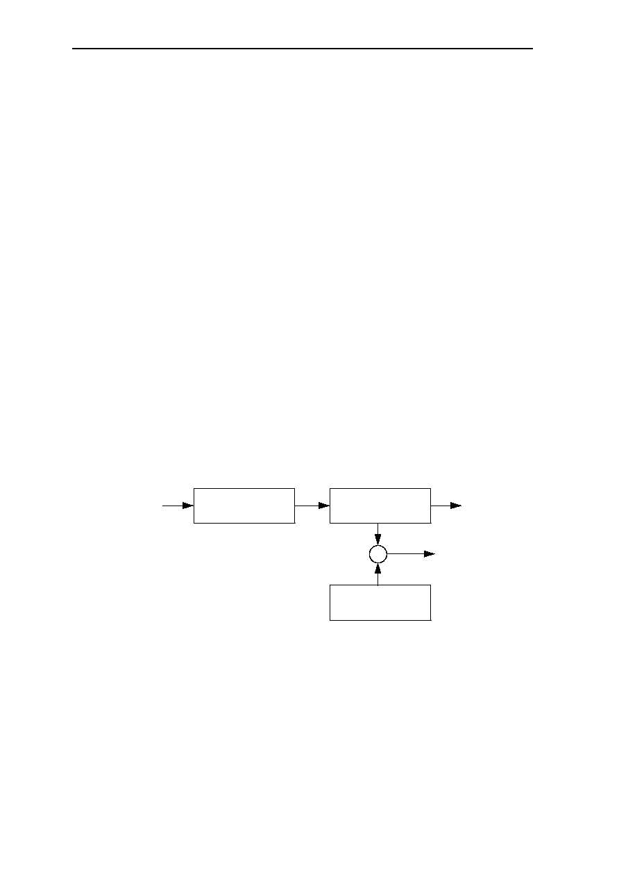
6-24 CHAPTER 6
6.7 Watchdog Compare Register WCR
Global register G24 is the watchdog compare register WCR. Only bits 15..0 are used, bits
31..16 are reserved, they must be zero on a move to the WCR. In the present version, bits
31..16 are read as zero. The WCR is used by the IO3 control modes (see section
6.8. IO3
Control Modes
).
6.8 IO3 Control Modes
Additionally to the standard use like IO1 and IO2 (see
section 6.9.3. Bus Signal
Description
), there are special control modes in combination with the IO3 pin. These
control modes are specified by FCR(13) and FCR(12).
On all IO3 control modes, the watchdog compare register WCR must be set before the
control mode is specified in the FCR, otherwise the EqualFlag could be set erroneously.
The EqualFlag and the EventFlag are being cleared on all IO3 control modes by either
setting FCR(13) to one or a move to the watchdog compare register WCR.
6.8.1 IO3Standard Mode
FCR(13) = 1, FCR(12) = 1 specifies IO3Standard mode.
Standard use of IO3 without any additional IO3 control functions. See section
6.9.3. for
signals IO1..IO3
.
6.8.2 Watchdog Mode
FCR(13) = 1, FCR(12) = 0 specifies Watchdog mode.
A Reset exception occurs when WCR(15..0) = TR(15..0). The standard use of IO3 is not
affected.
TR
WCR
x
Reset Exception
TPR
Processor Clock
Frequency
Timer Clock
Frequency
carry
compare
Note: The WCR must be set before the IO3 control mode is determined by FCR(13..12) as
Watchdog mode.

BUS INTERFACE 6-25
6.8.3 IO3Timing Mode
FCR(13) = 0, FCR(12) = 1 specifies the IO3Timing mode.
On IO3Direction = Input:
When input signal IO3Level = IO3Polarity, the EventFlag ISR(8) is set and the current
contents of the TR(15..0) is copied to the WCR. Thus, the time of the event indicated by
the 16 low-order bits of the TR is captured in the WCR. When WCR(15..0) = TR(15..0)
before the EventFlag is set, the EqualFlag ISR(7) is set. Either flag set causes an interrupt
when the IO3 interrupt is enabled.
Note: The EventFlag and the EqualFlag can be used to distinguish between an input signal
transition and a timeout. The EventFlag can be set even after the EqualFlag (but not vice
versa) during the interrupt latency time; thus, when the EventFlag is set, WCR(15..0)
contains always the time when the input reached the level specified by IO3Polarity. Note
that the EventFlag is immediately set on entering IO3Timing mode when the input signal is
already on the specified level. WCR(15..0) must be set on a value different from the value
of the TR(15..0), otherwise the EqualFlag is set immediately. The maximum span for the
timeout is 2
16
-1 ticks of the TR.
IO3Direction = Output:
When WCR(15..0) = TR(15..0), the EqualFlag is set and an interrupt occurs when the IO3
interrupt is enabled. Additionally, an internal toggle latch is toggled. The IO3 output signal
is high when the value of the toggle latch and IO3Polarity are not equal, otherwise low.
Thus, each toggling causes a transition of the IO3 output signal. The toggle latch is cleared
by setting FCR(13) to 1.
Note: This mode can be used to create an arbitrary output signal sequence by just updating
the WCR. When the program switches to IO3Standard mode after the end of a signal
sequence and the toggle latch remained set to 1, FCR(13) must be set to 1 and IO3Polarity
be inverted coincidentally in the same move to FCR to avoid a transition of the IO3 output
signal. The IO3 interrupt must also be disabled in the same move to FCR to avoid an
interrupt from the output signal.
6.8.4 IO3TimerInterrupt Mode
FCR(13) = 0, FCR(12) = 0 specifies the IO3TimerInterrupt mode.
Additionally to the standard use of IO3, the condition WCR(15..0) = TR(15..0) sets the
EqualFlag ISR(7) and causes an IO3 interrupt regardless of the IO3Mask in FCR(8) (IO3
interrupt disable).
Note: When the IO3 interrupt is disabled, the IO3TimerInterrupt mode can be used
independently of the use of IO3 as input or output. When the IO3 interrupt is enabled, the
IO3TimerInterrupt mode can be used as a timeout for the IO3 interrupt. The EqualFlag can
then be used to distinguish between timeout and an IO3 interrupt.

6-26 CHAPTER 6
6.9 Bus Signals
6.9.1 Bus Signals for the GMS30C2232 Processor
The following table is an overview of the bus signals of the
GMS30C2232
microprocessor.
For a detailed description of the function of the bus signals refer to section
6.9.3. Bus
Signal Description
.
The signal states are defined as I = input, O = output and Z = three-state (inactive).
States
Pin count Signal Name
Description
I
1
XTAL1/CLKIN
External Crystal, optionally Clock Input
O
1
XTAL2
External Crystal
O
1
CLKOUT
Clock Output
O/Z
26
A25..A0
Address Bus
O/I
32
D31..D0
Data Bus
O/I
4
DP0..DP3
Parity bits
O/Z
1
RAS#
DRAM RAS signal / Chip Select for MEM0
O/Z
4
CAS0#..CAS3#
DRAM CAS signal for bytes 0..3
O/Z
1
WE#
Write Enable for DRAM and R/W# for I/O
O/Z
3
CS1#..CS3#
Chip Select for MEM1..MEM3
O/Z
4
WE0#..WE3#
Write Enable/Byte Enable for SRAM bytes 0..3
O/Z
1
OE#
Output Enable for SRAMs, EPROMs, EDO DRAMs
O/Z
1
IORD#
I/O Read Strobe, optionally I/O Data Strobe
O/Z
1
IOWR#
I/O Write Strobe
O
1
RQST
Bus Request Output
I
1
GRANT#
Bus Grant Input
O
1
ACT
Active as Bus Master
I
3
INT1..INT2, INT4 Interrupt Inputs
I
1
INT3/WAIT
Interrupt Input or Wait Input
O/I
3
IO1..IO3
Programmable Input / Output
I
2
BOOTW, BOOTB Boot bus width selection inputs for MEM3
I
1
RESET#
Reset Input
16
NC
No Connect (not for GMS30C2232-144TQFP)
26
VDD
Power Supply Voltage
26
GND
Ground
Total:
160 (144 for GMS30C2232-144TQFP)
Table 6.9: Bus Signals for the GMS30C2232 Processor

BUS INTERFACE 6-27
6.9.2 Bus Signals for the GMS30C2216 Processor
The following table is an overview to the bus signals of the
GMS30C2216
microprocessor.
For detailed description of the function of the bus signals refer to section
6.9.3. Bus Signal
Description
.
The signal states are defined as I = input, O = output and Z = three-state (inactive).
States Pin count Signal-Names
Description
I
1
XTAL1/CLKIN
External Crystal, optionally Clock Input
O
1
XTAL2
External Crystal
O
1
CLKOUT
Clock Output
O/Z
22
A21..A0
Address Bus
O/I
16
D15..D0
Data Bus
O/I
2
DP0..DP1
Parity bits
O/Z
1
RAS#
DRAM RAS signal / Chip Select for MEM0
O/Z
2
CAS0#..CAS1#
DRAM CAS signal for bytes 0..1 / 2..3
O/Z
1
WE#
Write Enable
O/Z
3
CS1#..CS3#
Chip Select for MEM1..MEM3
O/Z
2
WE0#..WE1#
Write Enable/Byte Enable for SRAM bytes 0..1 / 2..3
O/Z
1
OE#
Output Enable for SRAMs, EPROMs, EDO DRAMs
O/Z
1
IORD#
I/O Read Strobe, optionally I/O Data Strobe
O/Z
1
IOWR#
I/O Write Strobe
O
1
RQST
Bus Request Output
I
1
GRANT#
Bus Grant Input
O
1
ACT
Active as Bus Master
I
3
INT1..INT2, INT4 Interrupt Inputs
I
1
INT3/WAIT
Interrupt Input or Wait Input
O/I
3
IO1..IO3
Programmable Input / Output
I
1
BOOTB
Boot bus width selection input for MEM3
I
1
RESET#
Reset Input
16
VDD
Power Supply Voltage
18
GND
Ground
Total:
100
Table 6.10: Bus Signals for the GMS30C2216 Processor

6-28 CHAPTER 6
6.9.3 Bus Signal Description
The following section describes the bus signals for both the
GMS30C2232
and
GMS30C2216
microprocessor in detail.
In the following signal description, the signal states are defined as I = input, O = output
and Z = three-state (inactive).
States Names Use
I XTAL1/CLKIN Input for quartz crystal. When the clock is generated by an
external clock generator, XTAL1 is used as clock input. The
clock signal is multiplied by four and divided according to the
TPR setting to generate the internal clock.
O XTAL2 Output for quartz crystal. XTAL2 is not connected when an
external clock generator is used.
O CLKOUT Clock signal output or programmable output. CLKOUT can be
selected as a programmable output pin or as output delivering
the CPU clock signal divided by 1, 2 or 4. CLKOUT can be
used to supply a clock signal to peripheral devices.
O/Z A25..A0 The address bits A25..A0 represent the address bus. An active
high bit signals a "one". A0 is the least significant bit. With the
E1-16
, only A21..A0 are connected to the address bus pins.
O/I D31..D0 Data bus. The signals D31..D0 (D15..D0 with the
GMS30C2216
)
represent the bidirectional data bus; active high signals a "one".
At a read access, data is transferred from the data bus to the
register set or to the instruction cache only at the cycle
corresponding to the last actual read access cycle, thus inhibiting
garbled data from being transferred.
At a write access, the data bus signals are activated during the
address setup, write and bus hold cycle(s).
A halfword or byte to be written is multiplexed from its right-
adjusted position in a register to the addressed halfword or byte
position. Thus, no external multiplexing of data signals is
required.
On a 32-bit wide memory area, byte addresses 0, 1, 2 and 3
correspond to D31..D24, D23..D16, D15..D8 and D7..D0
respectively (big endian).
On a 16-bit wide memory area, byte address 2 and 3 in the first
access and byte addresses 0 and 1 in the second access
correspond to D15..D8 and D7..D0 respectively.
On a 8-bit wide memory area, byte addresses 3..0 correspond to
D7..D0 in succeeding accesses.

BUS INTERFACE 6-29
States Names Use
O/I DP0..DP3 Data Parity signals. DP0..DP3 represent the bidirectional parity
signals; active high indicates a "one". With the
GMS30C2232
,
DP0, DP1, DP2 and DP3 correspond to D31..D24, D23..D16,
D15..D8 and D7..D0 respectively. With the
GMS30C2216
, DP0
and DP1 correspond to D15..D8 and D7..D0 respectively.
At a write access, all data parity signals are activated during the
address setup, write and bus hold cycles.
At a read access, the corresponding data parity signals are
evaluated at the last read access cycle when parity checking for
the addressed memory area is enabled.
Parity "odd" is used, that is, the correct parity bit is "one" when
all bits of the corresponding byte are "zero".
O/Z RAS# Row Address Strobe. Active low indicates row address strobe
asserted.
RAS# is activated high and then again low when the processor
accesses a new page in the DRAM address space, that is when
any of the (high order) RAS address bits is different from the
RAS address bits of the last DRAM access. RAS# is left low
after any own DRAM access.
RAS# is activated high, low and then high by a refresh cycle.
When the bus is granted to another bus master, the processor
starts the next DRAM access as a RAS access.
At any non-RAS address cycle, RAS# is left unchanged, thus, a
previously selected DRAM page is not affected.
When non-DRAM memory is placed in memory area MEM0,
RAS# is used as the chip select signal for this memory.
O/Z CAS0#..CAS3# Column Address Strobe. Active low indicates column address
strobe asserted. CAS0#..CAS3# are only used by a DRAM for
column access cycles and for "CAS before RAS" refresh.
With the
GMS30C2232
, CAS0#..CAS3# correspond to the
column address enable signals for D31..D24, D23..D16,
D15..D8 and D7..D0 respectively.
With the
GMS30C2216
, CAS0# and CAS1# correspond to the
column address enable signals for D15..D8 and D7..D0
respectively.
O/Z WE# Write Enable. WE# is signaled in the same cycle(s) as address
signals. Active low indicates a write access, active high
indicates a read access.
WE# is intended to be used as DRAM Write Enable and as
R/W# for I/O access when IORD# is specified as data strobe
(see IORD#).
Note: WE# can also be used to control bus transceivers when
peripheral devices or slow memories must be separated from the
processor data bus in order to decrease the capacitive load of the
processor data bus.

6-30 CHAPTER 6
States Names Use
O/Z CS1#..CS3# Chip Select. Chip select is signaled in the same cycle(s) as the
address signals. Active low of CS1#..CS3# indicates chip select
for the memory areas MEM1..MEM3 respectively.
Note: RAS# is used as chip select for a non-DRAM memory in
MEM0.
O/Z WE0#/BE0# SRAM Write Enable. Active low indicates write enable for the
..WE3#/BE3# corresponding byte, active high indicates write disable.
When the byte mode for the corresponding memory area is
enabled, WE0#..WE3# are used as byte enables BE0#..BE3#;
low indicates enable, high indicates disable. The WE# signal is
then used as write enable signals.
With the GMS30C2232, WE0#..WE3# correspond to the enable
signals for D31..D24, D23..D16, D15..D8 and D7..D0
respectively.
With the
GMS30C2216
, WE0# and WE1# correspond to the
enable signals for D15..D8 and D7..D0 respectively.
O/Z OE# Output Enable for SRAMs, EPROMs and EDO DRAMs. OE# is
active low on a SRAM, EPROM or EDO DRAM read access.
O/Z IORD# I/O Read Strobe, optionally I/O data strobe. The use of IORD#
is specified in the I/O address. Bit 10 = 0 specifies I/O read
strobe, bit 10 = 1 specifies I/O data strobe. When specified as
I/O read strobe, IORD# is low on I/O read access cycles, high
on all other cycles. When specified as I/O data strobe, IORD# is
low on any I/O access cycles, high on all other cycles.
Note: When IORD# is specified as I/O data strobe, WE# can be
used as R/W# signal.
O/Z IOWR# I/O Write Strobe. When specified as I/O writes strobe by I/O
address bit 10 = 0, IOWR# is active low on I/O write access
cycles.
O RQST RQST signals the request for a memory or I/O access. RQST is
high from the beginning of the request until the requested access
is completed.
I GRANT# Bus Grant. GRANT# is signaled low by an (off-chip) bus arbiter
to grant access to the bus for memory and I/O cycles. When
Grant# is switched from low to high during an access, the bus is
only released to another bus master after completion of the
current access. The GRANT# signal supplied by a bus arbiter
may be asynchronous to the clock; it is synchronized on-chip to
avoid metastable. For systems with a single bus master,
GRANT# must be tied low.
Note: GRANT# is recommended to be kept low by the bus
arbiter on the bus master with the last access; thus, any
subsequent access by the same bus master saves the
synchronization time.

BUS INTERFACE 6-31
States Names Use
O ACT Active as bus master. ACT is signaled high when GRANT# is
low and it is kept high during a current bus access. Since
GRANT# is asynchronous, ACT follows GRANT# with a delay
of 2..3 cycles. ACT is also kept high on a bus lock
(FCR(17) = 0) from the beginning of the first access after
FCR(17) is cleared to zero until the bus lock is released by
setting FCR(17) to one.
Note: When ACT transits from high to low, the address and data
bus are switched to three state (inactive). All bus control signals
marked O/Z are driven high and then switched to three state.
These signals are kept high by an on-chip resistor (ca. 1 M
)
tied on-chip to Vcc.
I INT1..INT4 Interrupt Request. A signal of a specified level on any of the
INT1..INT4 interrupt request pins causes an interrupt exception
when the interrupt lock flag L is zero and the corresponding
INTxMask bit in FCR is not set. The INTxPolarity bits in FCR
specify the level of the INTx signals: INTxPolarity = 1 causes
an interrupt on a high input signal level, INTxPolarity = 0
causes an interrupt on a low input signal level. INT1..INT4 may
be signaled asynchronously to the clock; they are not stored
internally.
A transition of INT1..INT4 is effective after a minimum of three
cycles. The response time may be much higher depending on the
number of cycles to the end of the current instruction or the
number of cycles until the interrupt lock flag L is cleared.
Note: The signal level of INT1..INT4 can be inspected in
ISR(0)..ISR(4). Thus, with the corresponding INTxMask bit set,
INT1..INT4 can be used just as input signals.
O/I IO1..IO3 General Input-Output. IO1..IO3 can be individually configured
via IOxDirection bits in the FCR as either input or output pins.
When configured as input, IO1..IO3 can be used like
INT1..INT4 for additional interrupt or input signals.
When configured as output, the IOxPolarity bit in FCR specifies
the output signal level. IOxPolarity = 1 specifies a high level,
IOxPolarity = 0 specifies a low level. IO1..IO3 are always
switched rail-to-rail regardless of the setting of MCR(25). An
output signal at IO1 or IO2 cannot cause an interrupt regardless
of the corresponding IOxMask bit; however, it can be inspected
as IOxLevel in ISR (e.g. for testing). IO3 can be used for
various control functions.
I RESET# Reset processor. RESET# low resets the processor to the initial
state and halts all activity. RESET# must be low for at least two
cycles. On a transition from low to high, a Reset exception
occurs and the processor starts execution at the Reset entry. The
transition may occur asynchronously to the clock.
O/Z BOOTW, Input pins for selecting the data bus width for boot memory area
BOOTB MEM3 (see section 6.1.1. Boot Width Selection).
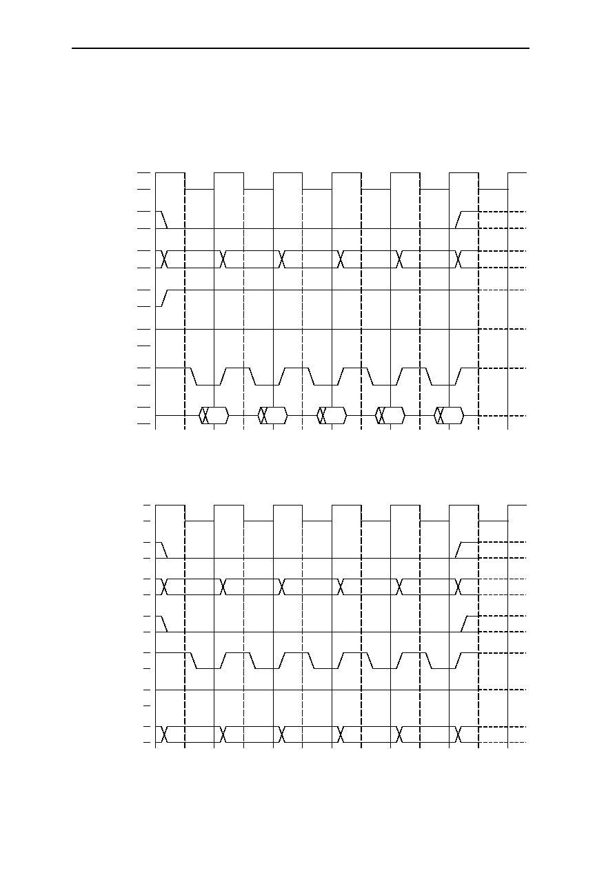
6-32 CHAPTER 6
6.10 Bus Cycles
6.10.1 MEMx Byte Mode = 1
6.10.1.1 SRAM and ROM Single-Cycle Read Access
Figure 6.2: SRAM and ROM Single-Cycle Read Access, MEMx Byte Mode = 1
6.10.1.2 SRAM Single-Cycle Write Access
Figure 6.3: SRAM Single-Cycle Write Access, MEMx Byte Mode = 1
CLK
Chip Select
Address Bus
WE#
WE0#..WE3#
Data Bus
(read data)
OE#
addr. 1
addr. 2
addr. 3
addr. 4
addr. 5
data 1
data 2
data 3
data 4
data 5
CLK
Chip Select
Address Bus
WE#
WE0#..WE3#
Data Bus
OE#
addr. 1
addr. 2
addr. 3
addr. 4
addr. 5
data 1
data 2
data 3
data 4
data 5
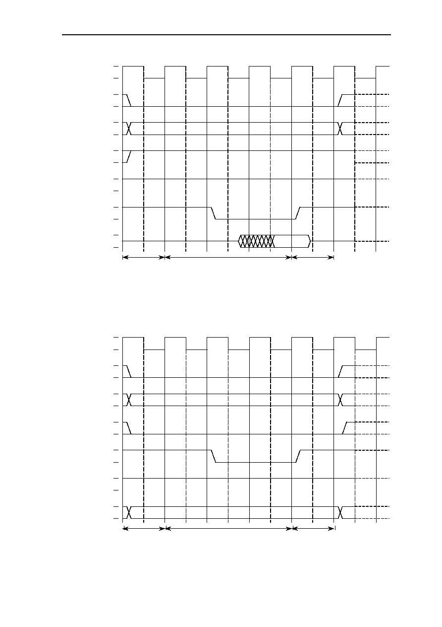
BUS INTERFACE 6-33
6.10.1.3 SRAM and ROM Multi-Cycle Read Access
Figure 6.4: SRAM and ROM Multi-Cycle Read Access, MEMx Byte Mode = 1
6.10.1.4 SRAM Multi-Cycle WriteAccess
Figure 6.5: SRAM Multi-Cycle Write Access, MEMx Byte Mode = 1
CLK
Chip Select
Address Bus
WE#
WE0#..WE3#
Data Bus
OE#
Address setup
time 0..3 cycles
Access time
2..16 cycles
Bus hold
time
0..7 cycles
Address setup
time 0..3 cycles
Access time
2..16 cycles
Bus hold
time
0..7 cycles
CLK
Chip Select
Address Bus
WE#
WE0#..WE3#
Data Bus
OE#
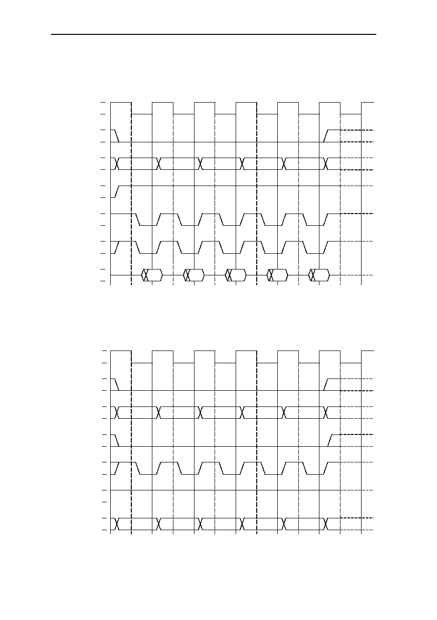
6-34 CHAPTER 6
6.10.2 MEMx Byte Mode = 0
6.10.2.1 SRAM Single-Cycle Read Access
Figure 6.6: SRAM Single-Cycle Read Access, MEMx Byte Mode = 0
6.10.2.2 SRAM Single-Cycle Write Access
Figure 6.7: SRAM Write-Cycle Read Access, MEMx Byte Mode = 0
CLK
Chip Select
Address Bus
WE#
BE0#..BE3#
Data Bus
(read data)
OE#
addr. 1
addr. 2
addr. 3
addr. 4
addr. 5
data 1
data 2
data 3
data 4
data 5
CLK
Chip Select
Address Bus
WE#
BE0#..BE3#
Data Bus
OE#
addr. 1
addr. 2
addr. 3
addr. 4
addr. 5
data 1
data 2
data 3
data 4
data 5
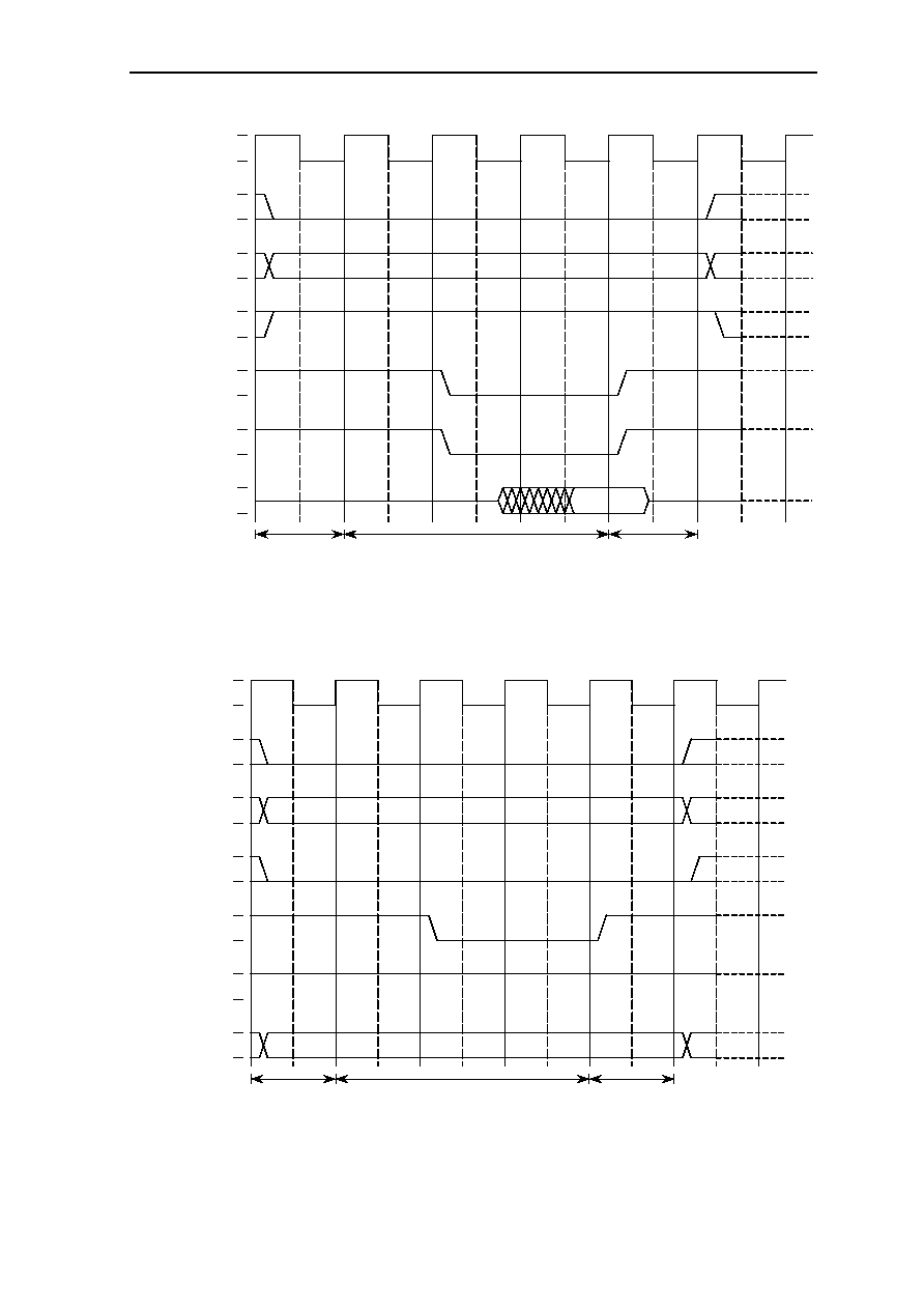
BUS INTERFACE 6-35
6.10.2.3 SRAM Multi-Cycle Read Access
Figure 6.8: SRAM Multi-Cycle Read Access, MEMx Byte Mode = 0
6.10.2.4 SRAM Multi-Cycle Write Access
Figure 6.9: SRAM Multi-Cycle Write Access, MEMx Byte Mode = 0
Address
setup time
0..3 cycles
Access
time 2..16
Bus hold
time
0..7 cycles
CLK
Chip Select
Address Bus
WE#
BE0#..BE3#
Data Bus
OE#
CLK
Chip Select
Address Bus
WE#
BE0#..BE3#
Data Bus
OE#
Address setup
time 0..3
cycles
Access
time 2..16
Bus hold time
0..7 cycles

6-36 CHAPTER 6
6.10.3 MEM2 Read Access with WAIT Pin
Figure 6.10: MEM2 Read Access with WAIT Pin
Note:
·
Arrows on WAIT signal indicate the times where the signal is inspected.
·
In this example
specified access time: 4 cycles
actual access time: 6 = 4 cycles + 2 additional cycles caused by WAIT pin
CLK
Chip Select
Address Bus
WE0#..WE3#
WAIT
Data Bus
OE#
Access time
(minimum 4 cycle)
Next access
or bus hold
time if specified
MEM2 Byte Mode = 1, INT3Polarity = Inverted,
address setup time = 0 cycles, bus hold time = 0 cycles
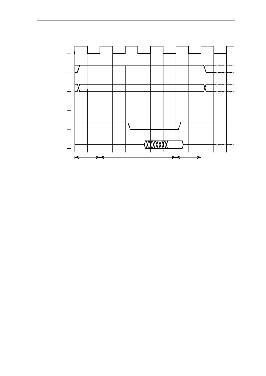
BUS INTERFACE 6-37
6.10.4 I/O Read Access
CLK
Chip Select
Address Bus
WE#
IORD#
Data Bus
Access time
2..16 cycles
Address
setup time
0..6 cycles
Bus hold
time
0..6 cycles
Figure 6.11: I/O Read Access
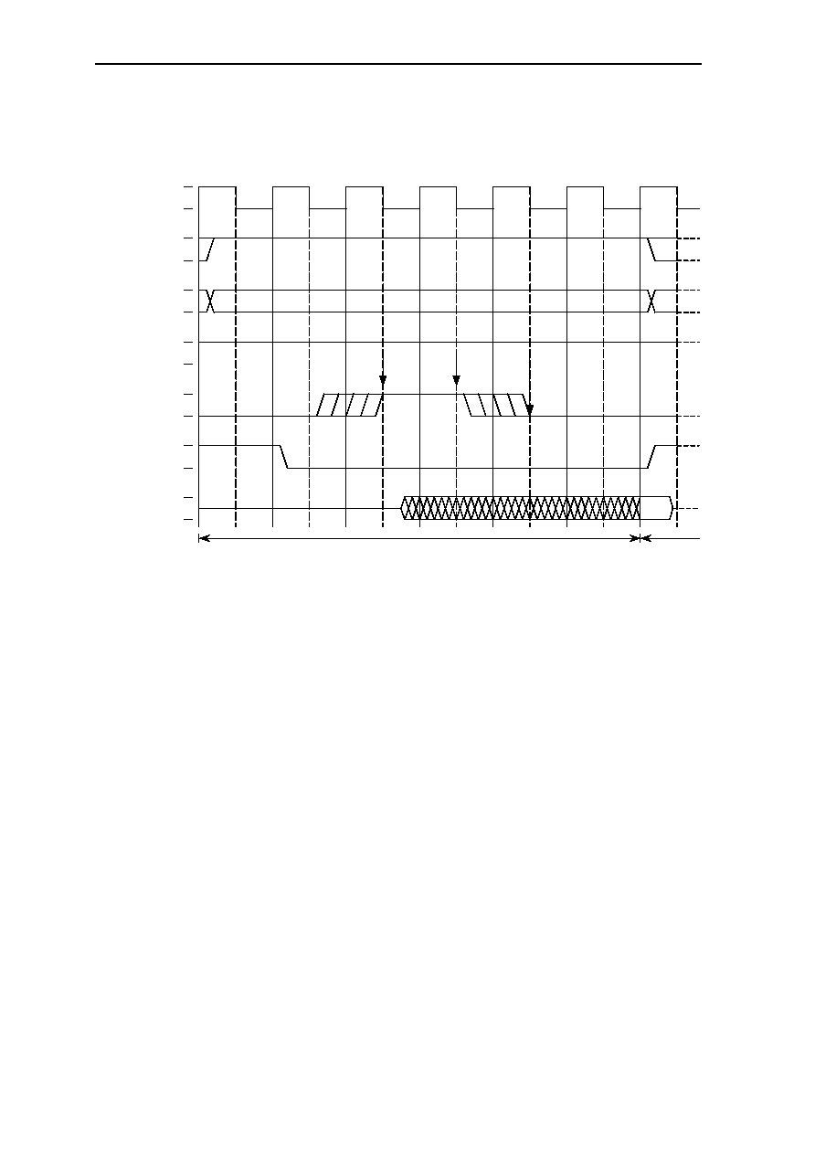
6-38 CHAPTER 6
6.10.5 I/O Read Access with WAIT Pin
Figure 6.12: I/O Read Access with WAIT Pin
Note:
·
Arrows on WAIT signal indicate the times where the signal is inspected.
·
In this example
specified access time: 4 cycles
actual access time: 6 = 4 cycles + 2 additional cycles caused by WAIT pin
CLK
Chip Select
Address Bus
WE#
WAIT
Data Bus
OE#
Access time
(minimum 4 cycle)
Next access
or bus hold
time if specified
address setup time = 0 cycles, bus hold time = 0 cycles, INT3Polarity =
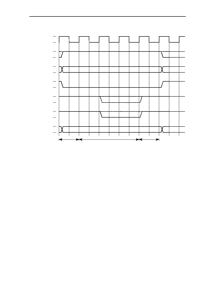
BUS INTERFACE 6-39
6.10.6 I/O Write Access
CLK
Chip Select
Address Bus
WE#
IORD#
Data Bus
Access time
2..16 cycles
Address
setup time
0..6 cycles
Bus hold
time
1..7 cycles
IOWR#
Figure 6.13: I/O Write Access
Note:
·
If IORD# is used as I/O data strobe, IORD# instead of IOWR# is activated low.
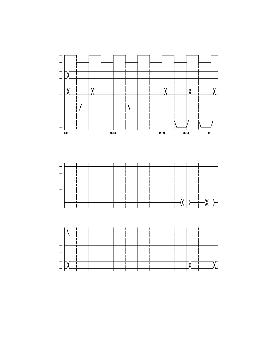
6-40 CHAPTER 6
6.10.7 DRAM
6.10.7.1 Fast Page Mode DRAM Access
Figure 6.14: Fast Page Mode DRAM Access
CLK
Address Bus
high order bits
Address Bus
low order bits
RAS#
CAS0#..CAS3#
RAS precharge time
1..6 cycles
RAS to CAS delay time
1..6 cycles
CAS access
time
1..6 cycles
CAS access
time
1..6 cycles
WE#
OE#
Data Bus
(read data)
at read access
WE#
OE#
Data Bus
(write data)
at write access
valid
undefine
Row address
col. addr. col. addr.
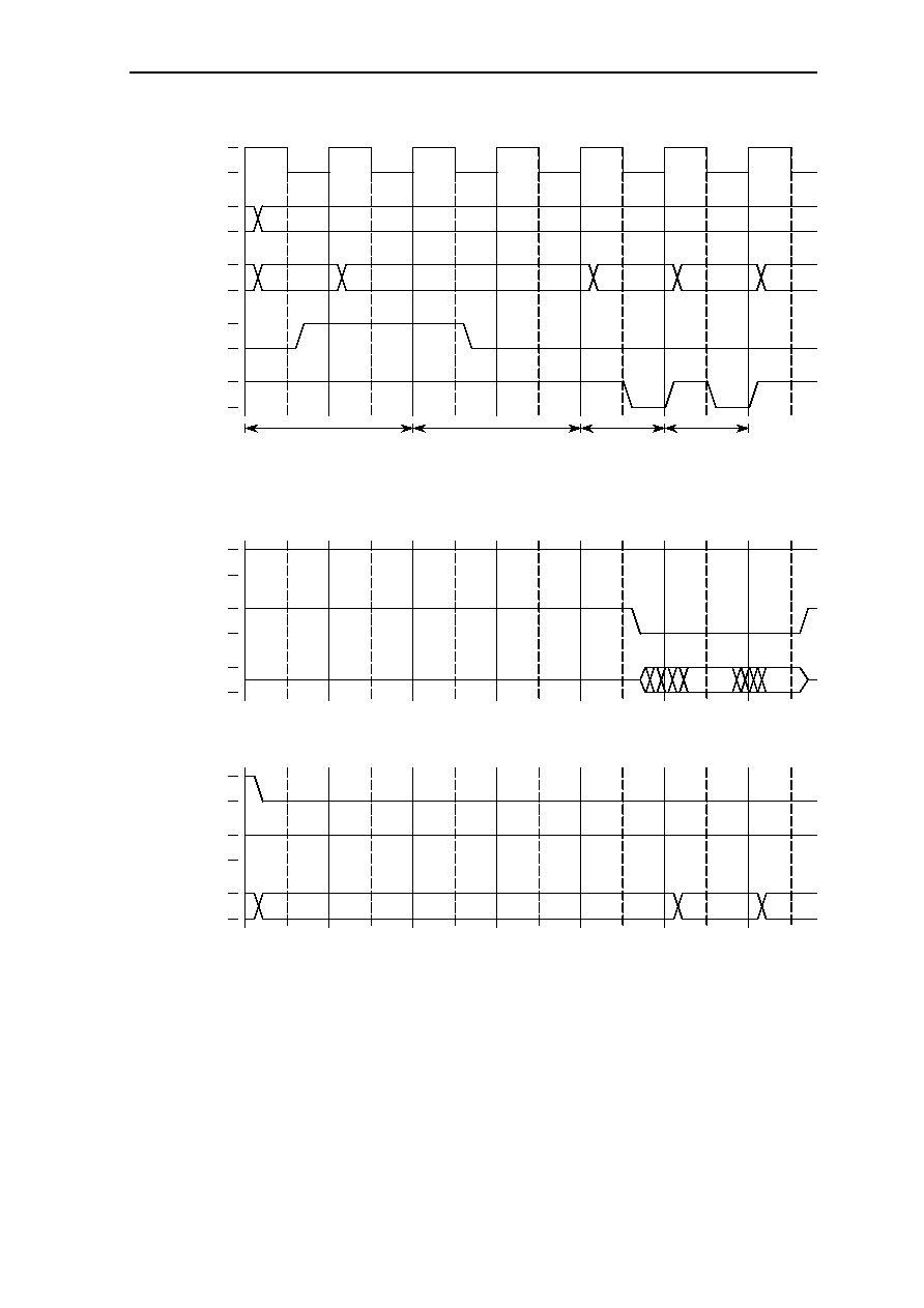
BUS INTERFACE 6-41
6.10.7.2 EDO DRAM Single-Cycle Access
Figure 6.15: EDO DRAM Single-Cycle Access
CLK
Address Bus
high order
bits
Address Bus
low order bits
RAS#
CAS0#..CAS3#
RAS precharge time
1..6 cycles
RAS to CAS delay time
1..6 cycles
CAS access
time
1..6 cycles
CAS access
time
1..6 cycles
WE#
OE#
Data Bus
(read data)
at read access
WE#
OE#
Data Bus
(write data)
at write access
valid
undefin
Row address
col. addr.
col. addr.
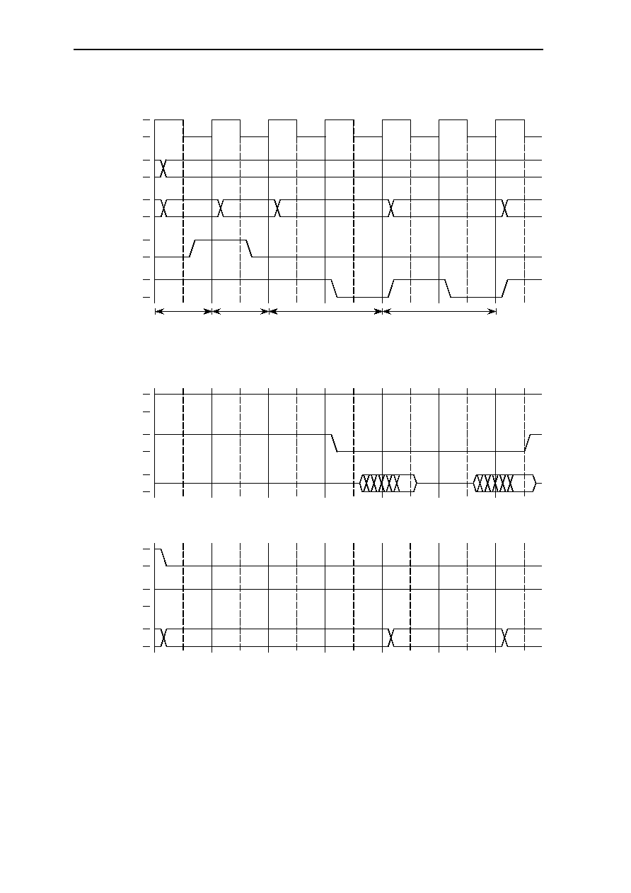
6-42 CHAPTER 6
6.10.7.3 EDO DRAM Multi-Cycle Access
Figure 6.16: EDO DRAM Multi--Cycle Access
CLK
Address Bus
high order
bits
Address Bus
low order bits
RAS#
CAS0#..CAS3#
CAS access time
1..6 cycles
CAS access time
1..6 cycles
RAS to CAS
delay time
1..4 cycles
RAS access
time
1..6 cycles
WE#
OE#
Data Bus
(read data)
at read access
WE#
OE#
Data Bus
(write data)
at write access
valid
undefin
row addr.
Column address
Column address
OE# is set after the first cycle of the CAS access time
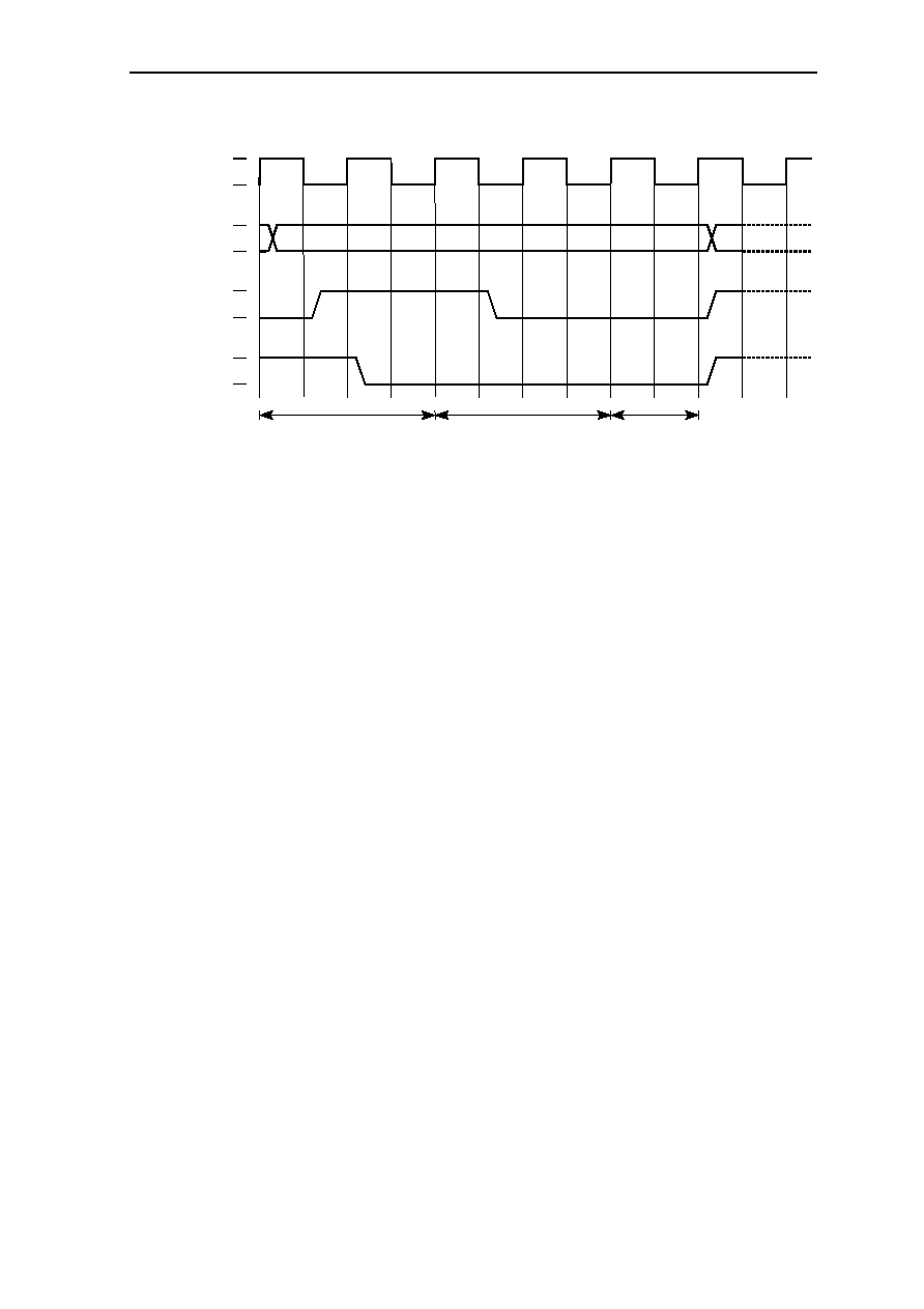
BUS INTERFACE 6-43
6.10.7.4 DRAM Refresh (CAS before RAS Refresh)
CLK
Address Bus
CAS#
RAS to CAS delay time
1..4 cycles
RAS precharge time
1..4 cycles
CAS access
time
1..6 cycles
RAS#
undefined
Figure 6.17: DRAM Refresh
6-44 CHAPTER 6
6.11 DC Characteristics
Absolute Maximum Ratings
Case temperature T
C
under Bias: 0°C to +70°C
extended temperature range on request
Storage Temperature: -65°C to +150°C
Voltage on any Pin with respect to ground: -0.5V to V
CC
+ 0.5V
D.C. Parameters
Supply Voltage V
CC
: 3.3V
±
0.30V
Case Temperature T
CASE
: 0°C to +85°C
Symbol
Parameter
MIN
MAX
UNIT
Notes
VIL
Input Low Voltage
-0.3
+0.8
V
except CLKIN
VIH
Input High Voltage
2.0
5V+0.5
V
except CLKIN
VOL
Output Low Voltage
0.45
V
at 4
§ Ì
VOH
Output High Voltage
2.4
V
at 4
§ Ì
ILI
Input Leakage Current
¡ ¾
20
§ Ë
ILO
Output Leakage Current
¡ ¾
20
§ Ë
C
CLK
Clock Capacitance
10
§ Ü
C
ADR
Output Capacitance
A12..A0
15
§ Ü
C
I
/
O
Input/output Capacitance all
other signals
10
§ Ü
Table 6.11: DC Characterist
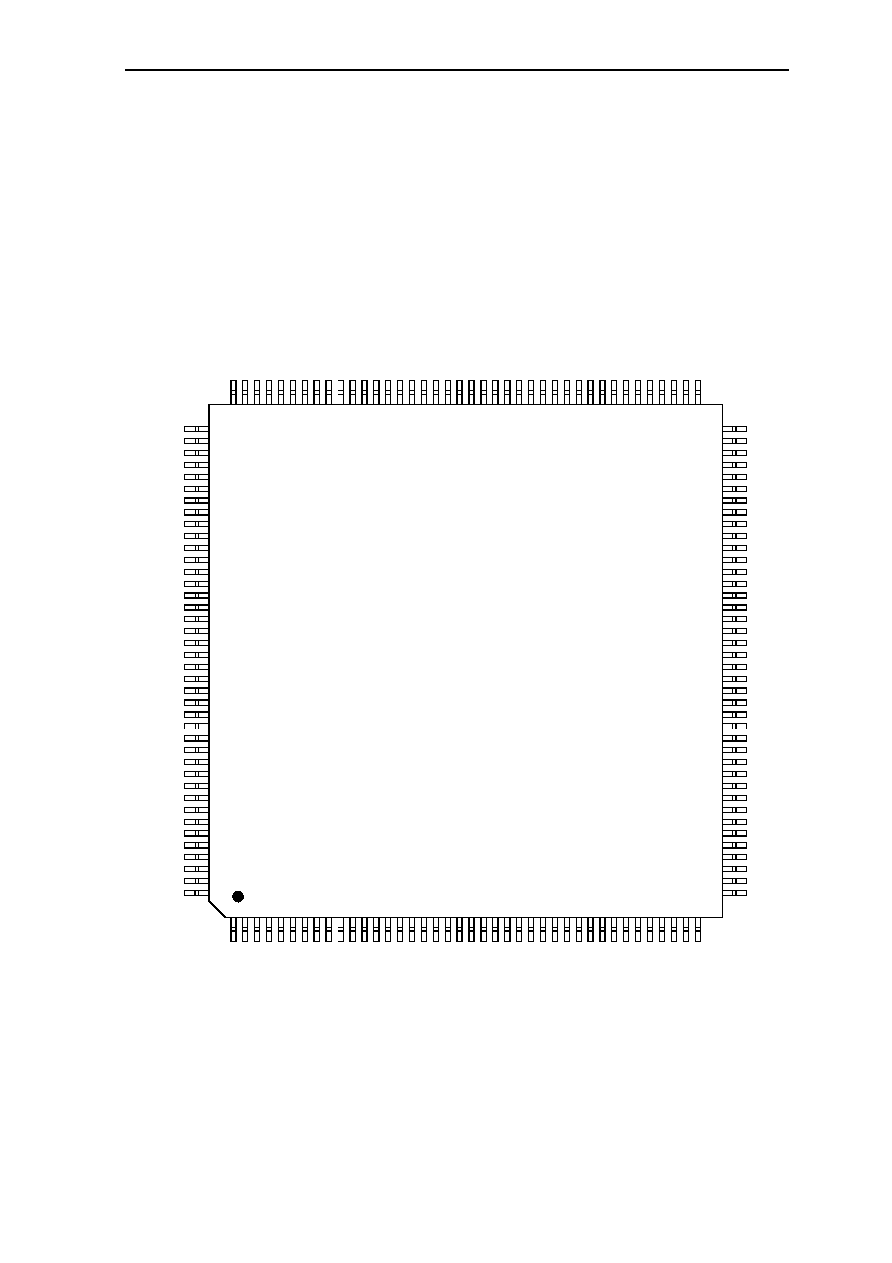
MECHANICAL DATA 7-1
7. Mechanical Data
7.1 GMS30C2232, 160-Pin MQFP-Package
7.1.1 Pin Configuration - View from Top Side
2
1
3
4
5
6
7
8
9
10
11
12
13
14
15
16
17
18
19
20
21
22
23
24
25
108
107
106
105
104
103
102
101
100
99
98
96
95
94
93
92
91
90
89
88
87
86
85
84
121
122
123
124
125
126
127
128
129
130
131
132
133
97
48
47
46
45
44
43
42
41
71
70
69
68
67
66
65
64
63
62
49
50
A24
A23
GND
VCC
A22
A8
A7
VCC
A6
A5
A4
GND
WE0#/BE0#
WE1#/BE1#
VCC
CAS0#
A14
GND
VCC
ACT
A13
GND
WE#
GND
VCC
VCC
D23
D22
GND
D5
D4
D3
VCC
D2
D1
D0
VCC
GND
D21
D20
D19
DP2
DP3
VCC
GND
RESET#
GRANT#
VCC
GND
VCC
VCC
GND
IO3
IO
WR#
CS3#
CS2#
CS1#
GND
RAS#
A19
VCC
A20
A21
GND
D31
D30
D29
A9
A10
A11
A12
VCC
D28
D27
D26
GND
W
E2#
/BE2#
IORD#
OE#
VCC
CAS3#
CAS2#
CAS1#
GND
XTAL1/CLKIN
XTAL2
IO2
VCC
D16
D17
D18
A3
A2
A1
A0
GND
DP1
DP0
83
82
81
BOOT
W
CLKOUT
IO1
GND
RQST
INT4
INT3
/WAIT
INT2
INT1
GND
VCC
61
60
59
58
57
56
55
54
53
52
51
VCC
GND
D9
GND
D8
D7
VCC
GND
D6
D24
26
27
28
29
30
31
32
33
34
35
36
GND
D25
D15
D14
VCC
D13
D12
D11
D10
GND
VCC
134
135
136
137
138
139
140
141
142
143
144
VCC
GND
BOOTB
A18
A17
GND
VCC
A16
A15
A25
GND
72
GND
VCC
W
E3#
/BE3#
NC
NC
NC
NC
109
110
111
112
113
114
115
116
117
118
119
120
73
74
75
76
77
78
79
80
NC
NC
NC
NC
37
38
39
40
NC
NC
NC
NC
145
146
147
148
149
150
151
152
153
154
155
156
157
158
159
160
NC
NC
NC
NC
GMS30C2232
Figure 7.1: GMS30C2232, 160-Pin MQFP-Package

7-2 CHAPTER 7
7.1.2 Pin Cross Reference by Pin Name
Signal Location Signal Location Signal Location Signal Location
A0 ................... 97 D3......................59 GND.................. 50 NC................... 118
A1 ................... 98 D4......................58 GND.................. 56 NC................... 123
A2 ................... 99 D5......................57 GND.................. 65 NC................... 124
A3 ................. 100 D6......................51 GND.................. 68 NC................... 157
A4 ................. 137 D7......................48 GND.................. 73 NC................... 158
A5 ................. 138 D8......................47 GND.................. 79 OE #................ 113
A6 ................. 139 D9......................45 GND.................. 82 RAS# ................ 11
A7 ................. 141 D10....................36 GND.................. 90 RESET# ............ 74
A8 ................. 142 D11....................35 GND.................. 96 RQST ................ 89
A9 ................... 20 D12....................34 GND................ 108 VCC .................... 1
A10 ................. 21 D13....................33 GND.................119 VCC .................. 13
A11 ................. 22 D14....................31 GND................ 122 VCC .................. 24
A12 ................. 23 D15....................30 GND................ 126 VCC .................. 32
A13 ............... 127 D16..................103 GND................ 130 VCC .................. 40
A14 ............... 131 D17..................102 GND................ 136 VCC .................. 41
A15 ............... 150 D18..................101 GND................ 145 VCC .................. 49
A16 ............... 151 D19....................69 GND................ 148 VCC .................. 53
A17 ............... 154 D20....................67 GND................ 153 VCC .................. 60
A18 ............... 155 D21....................66 GND................ 159 VCC .................. 64
A19 ................. 12 D22....................55 GRANT# ........... 75 VCC .................. 72
A20 ................. 14 D23....................54 INT1.................. 85 VCC .................. 76
A21 ................. 15 D24....................52 INT2.................. 86 VCC .................. 80
A22 ............... 143 D25....................29 INT3/WAIT........ 87 VCC .................. 81
A23 ............... 146 D26....................27 INT4.................. 88 VCC ................ 104
A24 ............... 147 D27....................26 IO1.................... 91 VCC ................ 112
A25 ............... 149 D28....................25 IO2.................. 105 VCC ................ 120
ACT .............. 128 D29....................19 IO3...................... 5 VCC ................ 121
BOOTB......... 156 D30....................18 IORD#..............114 VCC ................ 129
BOOTW.......... 93 D31....................17 IOWR#................ 6 VCC ................ 133
CAS0# .......... 132 DP0 ...................94 NC ...................... 3 VCC ................ 140
CAS1# .......... 109 DP1 ...................95 NC ...................... 4 VCC ................ 144
CAS2# .......... 110 DP2 ...................70 NC .................... 37 VCC ................ 152
CSS3# .......... 111 DP3 ...................71 NC .................... 38 VCC ................ 160
CLKOUT
...... 92 GND ....................2 NC .................... 43 WE# ................ 125
CS1# ................ 9 GND ..................10 NC .................... 44 WE0#/BE0# .... 135
CS2#
................ 8 GND ..................16 NC .................... 77 WE1#/BE1# .... 134
CS3# ................ 7 GND ..................28 NC .................... 78 WE2#/BE2# .... 115
D0................... 63 GND ..................39 NC .................... 83 WE3#/BE3# .... 116
D1................... 62 GND ..................42 NC .................... 84 XTAL1/CLKIN . 107
D2................... 61 GND ..................46 NC ...................117 XTAL2 ............. 106

MECHANICAL DATA 7-3
7.1.3 Pin Cross Reference by Location
Location Signal Location Signal Location Signal Location Signal
1 .......VCC 41....... VCC 81....... VCC 121....... VCC
2 .......GND 42....... GND 82....... GND 122....... GND
3 .......NC 43....... NC 83....... NC 123....... NC
4 .......NC 44....... NC 84....... NC 124....... NC
5 .......IO3 45....... D9 85....... INT1 125....... WE#
6 .......IOWR# 46....... GND 86....... INT2 126....... GND
7 .......CS3# 47....... D8 87....... INT3/WAIT 127....... A13
8 .......CS2# 48....... D7 88....... INT4 128....... ACT
9 .......CS1# 49....... VCC 89....... RQST 129....... VCC
10 .......GND 50....... GND 90....... GND 130....... GND
11.......RAS# 51....... D6 91....... IO1 131....... A14
12 .......A19 52....... D24 92....... CLKOUT 132....... CAS0#
13 .......VCC 53....... VCC 93....... BOOTW 133....... VCC
14 .......A20 54....... D23 94....... DP0 134....... WE1#/BE1#
15 .......A21 55....... D22 95....... DP1 135....... WE0#/BE0#
16 .......GND 56....... GND 96....... GND 136....... GND
17 .......D31 57....... D5 97....... A0 137....... A4
18 .......D30 58....... D4 98....... A1 138....... A5
19 .......D29 59....... D3 99....... A2 139....... A6
20 .......A9 60....... VCC 100....... A3 140....... VCC
21 .......A10 61....... D2 101....... D18 141....... A7
22 .......A11 62....... D1 102....... D17 142....... A8
23 .......A12 63....... D0 103....... D16 143....... A22
24 .......VCC 64....... VCC 104....... VCC 144....... VCC
25 .......D28 65....... GND 105....... IO2 145....... GND
26 .......D27 66....... D21 106....... XTAL2 146....... A23
27 .......D26 67....... D20 107....... XTAL1/CLKIN 147....... A24
28 .......GND 68....... GND 108....... GND 148....... GND
29 .......D25 69....... D19 109....... CAS1# 149....... A25
30 .......D15 70....... DP2 110....... CAS2# 150....... A15
31 .......D14 71....... DP3 111....... CAS3# 151....... A16
32 .......VCC 72....... VCC 112....... VCC 152....... VCC
33 .......D13 73....... GND 113....... OE# 153....... GND
34 .......D12 74....... RESET# 114....... IORD# 154....... A17
35 .......D11 75....... GRANT# 115....... WE2#/BE2# 155....... A18
36 .......D10 76....... VCC 116....... WE3#/BE3# 156....... BOOTB
37 .......NC 77....... NC 117....... NC 157....... NC
38 .......NC 78....... NC 118....... NC 158....... NC
39 .......GND 79....... GND 119....... GND 159....... GND
40 .......VCC 80....... VCC 120....... VCC 160....... VCC
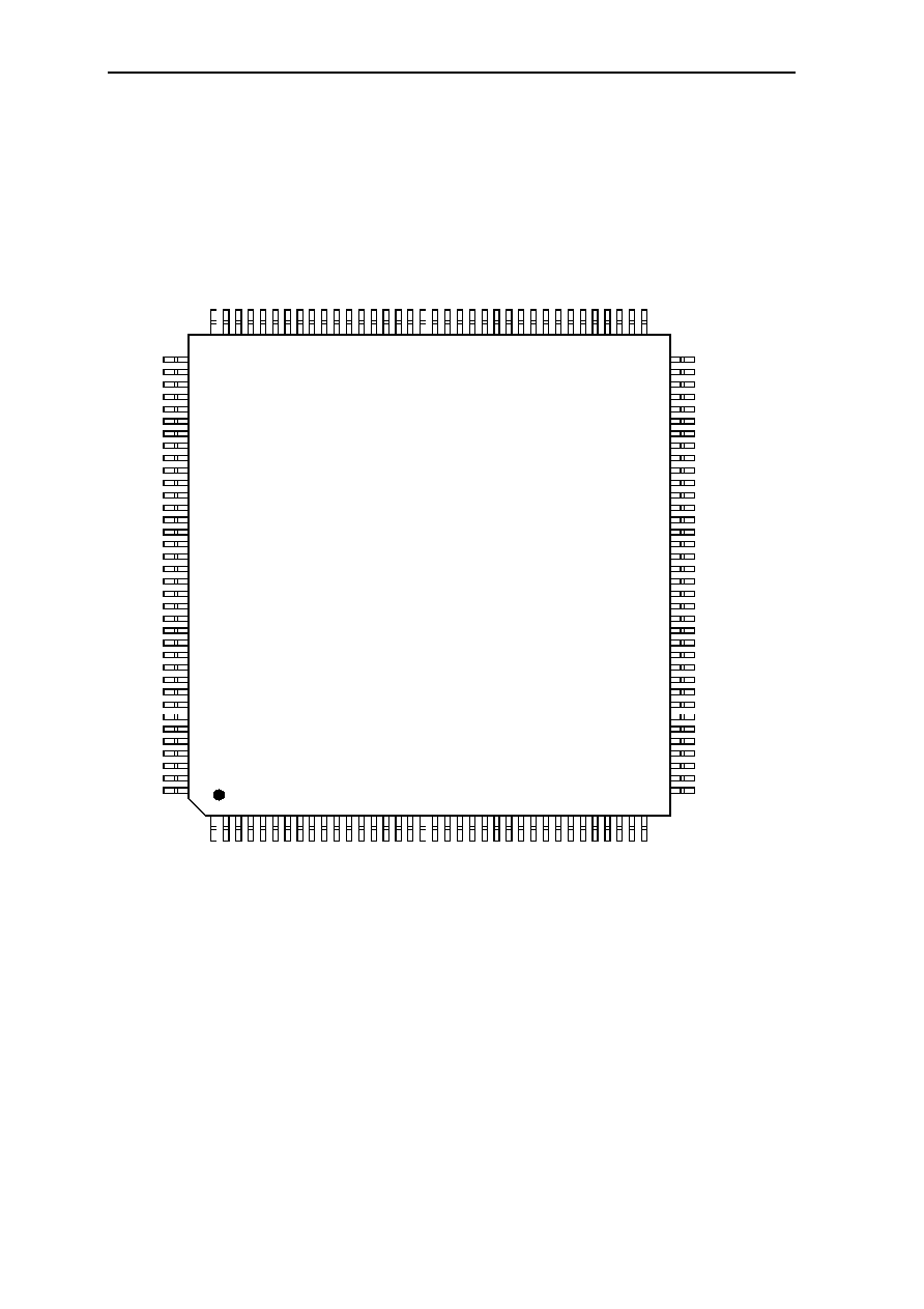
7-4 CHAPTER 7
7.2 GMS30C2232, 144-Pin TQFP-Package
7.2.1 Pin Configuration - View from Top Side
2
1
3
4
5
6
7
8
9
10
11
12
13
14
15
16
17
18
19
20
21
22
23
24
25
108
107
106
105
104
103
102
101
100
99
98
96
95
94
93
92
91
90
89
88
87
86
85
123
124
125
126
127
128
129
130
131
132
133
97
48
47
46
45
44
43
71
70
69
68
67
66
65
64
63
62
49
50
A20
A21
GND
D31
D30
D29
A9
A10
A11
A12
VCC
D28
D27
D26
GND
D25
D15
D14
VCC
D13
D12
D11
D10
GND
VCC
GND
XTAL1/CLKIN
XTAL2
IO2
VCC
D16
D17
D18
A3
A2
A1
A0
GND
DP1
DP0
CLKOUT
IO1
GND
RQST
INT4
INT3
INT2
INT1
GND
VCC
VCC
GND
BOOTB
A18
A17
GND
VCC
A16
A15
A25
GND
A24
A23
GND
VCC
A22
A8
A7
VCC
A6
A5
A4
GND
W
E0#
/BE0#
W
E1#
/BE1#
GND
GND
D8
D7
VCC
GND
D6
D24
VCC
D23
D22
GND
D5
D4
D3
VCC
D2
D1
D0
VCC
GND
D21
D20
84
83
GND
D19
DP2
DP3
VCC
GND
RESET#
GRANT#
VCC
GND
VCC
61
60
59
58
57
56
55
54
53
52
51
VCC
GND
WE3#
WE2#
IORD#
OE#
VCC
CAS3#
CAS2#
CAS1#
26
27
28
29
30
31
32
33
34
35
36
VCC
CAS0#
A14
GND
VCC
ACT
A13
GND
W
E#
GND
VCC
134
135
136
137
138
139
140
141
142
143
144
VCC
GND
IO3
IOWR#
CS3#
CS2#
CS1#
GND
RAS#
A19
VCC
72
BOOTW
VCC
D9
GMS30C2232
42
41
40
39
38
37
82
81
80
79
78
77
76
75
74
73
109
110
111
112
113
114
115
116
117
118
119
120
121
122
Figure 7.2: GMS30C2232, 144-Pin TQFP-Package

MECHANICAL DATA 7-5
7.2.2 Pin Cross Reference by Pin Name
Signal Location Signal Location Signal Location Signal Location
A0................... 58 CS3# ...............140 DP3 .................. 80 IOWR# ............ 141
A1................... 57 D0 .....................88 GND ................... 2 OE#................... 42
A2................... 56 D1 .....................89 GND ................... 6 RAS# .............. 136
A3................... 55 D2 .....................90 GND ..................11 RESET#............ 77
A4................... 22 D3 .....................92 GND ................. 14 RQST................ 66
A5................... 21 D4 .....................93 GND ................. 23 VCC .................... 1
A6................... 20 D5 .....................94 GND ................. 29 VCC .................... 7
A7................... 18 D6 ...................100 GND ................. 33 VCC .................. 15
A8................... 17 D7 ...................103 GND ................. 35 VCC .................. 19
A9................. 127 D8 ...................104 GND ................. 38 VCC .................. 26
A10............... 126 D9 ...................106 GND ................. 47 VCC .................. 30
A11 ............... 125 D10 ................. 111 GND ................. 59 VCC .................. 36
A12............... 124 D11.................. 112 GND ................. 65 VCC .................. 37
A13................. 32 D12 ................. 113 GND ................. 71 VCC .................. 43
A14................. 28 D13 ................. 114 GND ................. 74 VCC .................. 51
A15................... 9 D14 ................. 116 GND ................. 78 VCC .................. 72
A16................... 8 D15 ................. 117 GND ................. 83 VCC .................. 73
A17................... 5 D16 ...................52 GND ................. 86 VCC .................. 75
A18................... 4 D17 ...................53 GND ................. 95 VCC .................. 79
A19............... 135 D18 ...................54 GND ............... 101 VCC .................. 87
A20............... 133 D19 ...................82 GND ............... 105 VCC .................. 91
A21............... 132 D20 ...................84 GND ............... 107 VCC .................. 98
A22................. 16 D21 ...................85 GND ................110 VCC ................ 102
A23................. 13 D22 ...................96 GND ................119 VCC ................ 108
A24................. 12 D23 ...................97 GND ............... 131 VCC ................ 109
A25................. 10 D24 ...................99 GND ............... 137 VCC ................ 115
ACT ................ 31 D25 ................. 118 GND ............... 143 VCC ................ 123
BOOTB............. 3 D26 .................120 GRANT#........... 76 VCC ................ 134
BOOTW.......... 62 D27 .................121 INT1.................. 70 VCC ................ 144
CAS0#............ 27 D28 .................122 INT2.................. 69 WE# .................. 34
CAS1#............ 46 D29 .................128 INT3/WAIT........ 68 WE0#/BE0# ...... 24
CAS2#............ 45 D30 .................129 INT4.................. 67 WE1#/BE1# ...... 25
CAS3#............ 44 D31 .................130 IO1.................... 64 WE2#/BE2# ...... 40
CLKOUT......... 63 DP0 ...................61 IO2.................... 50 WE3#/BE3# ...... 39
CS1# ............ 138 DP1 ...................60 IO3.................. 142 XTAL1/CLKIN ... 48
CS2# ............ 139 DP2 ...................81 IORD # ............. 41 XTAL2 ............... 49

7-6 CHAPTER 7
7.2.3 Pin Cross Reference by Location
Location Signal Location Signal Location Signal Location Signal
1 .......VCC 37 .......VCC 73 ....... VCC 109....... VCC
2 .......GND 38 .......GND 74 ....... GND 110....... GND
3 .......BOOTB 39 .......WE3#/BE3# 75 ....... VCC 111....... D10
4 .......A18 40 .......WE2#/BE2# 76 ....... GRANT# 112....... D11
5 .......A17 41 .......IORD# 77 ....... RESET# 113....... D12
6 .......GND 42 .......OE# 78 ....... GND 114....... D13
7 .......VCC 43 .......VCC 79 ....... VCC 115....... VCC
8 .......A16 44 .......CAS3# 80 ....... DP3 116....... D14
9 .......A15 45 .......CAS2# 81 ....... DP2 117....... D15
10 .......A25 46 .......CAS1# 82 ....... D19 118....... D25
11 .......GND 47 .......GND 83 ....... GND 119....... GND
12 .......A24 48 .......XTAL1/CLKIN 84 ....... D20 120....... D26
13 .......A23 49 .......XTAL2 85 ....... D21 121....... D27
14 .......GND 50 .......IO2 86 ....... GND 122....... D28
15 .......VCC 51 .......VCC 87 ....... VCC 123....... VCC
16 .......A22 52 .......D16 88 ....... D0 124....... A12
17 .......A8 53 .......D17 89 ....... D1 125....... A11
18 .......A7 54 .......D18 90 ....... D2 126....... A10
19 .......VCC 55 .......A3 91 ....... VCC 127....... A9
20 .......A6 56 .......A2 92 ....... D3 128....... D29
21 .......A5 57 .......A1 93 ....... D4 129....... D30
22 .......A4 58 .......A0 94 ....... D5 130....... D31
23 .......GND 59 .......GND 95 ....... GND 131....... GND
24 .......WE0#/BE0# 60 .......DP1 96 ....... D22 132....... A21
25 .......WE1#/BE1# 61 .......DP0 97 ....... D23 133....... A20
26 .......VCC 62 .......VCC 98 ....... VCC 134....... VCC
27 .......CAS0# 63 .......CLKOUT 99 ....... D24 135....... A19
28 .......A14 64 .......IO1 100 ....... D6 136....... RAS#
29 .......GND 65 .......GND 101 ....... GND 137....... GND
30 .......VCC 66 .......RQST 102 ....... VCC 138....... CS1#
31 .......ACT 67 .......INT4 103 ....... D7 139....... CS2#
32 .......A13 68 .......INT3 104 ....... D8 140....... CS3#
33 .......GND 69 .......INT2 105 ....... GND 141....... IOWR#
34 .......WE# 70 .......INT1 106 ....... D9 142....... IO3
35 .......GND 71 .......GND 107 ....... GND 143....... GND
36 .......VCC 72 .......VCC 108 ....... VCC 144....... VCC
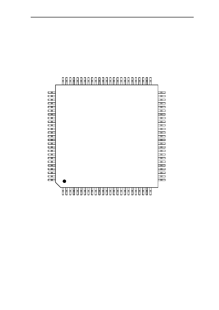
MECHANICAL DATA 7-7
7.3 GMS30C2216, 100-Pin TQFP-Package
7.3.1 Pin Configuration - View from Top Side
2
1
3
4
5
6
7
8
9
10
11
12
13
14
15
16
17
18
19
20
21
22
23
24
25
75
74
73
72
71
70
69
68
67
66
65
63
62
61
60
59
58
57
56
55
54
53
90
91
92
93
94
95
96
97
98
99
100
64
37
36
35
34
33
32
38
39
A20
A21
GND
A9
A10
A11
A12
VCC
GND
D15
D14
VCC
D13
D12
D11
D10
GND
XTAL1/CLKIN
XTAL2
IO2
VCC
A3
A2
A1
A0
GND
CLKOUT
IO1
GND
RQST
INT4
INT3/WAIT
INT2
INT1
BOOTB
A18
A17
GND
VCC
A16
A15
GND
GND
VCC
A8
A7
VCC
A6
A5
A4
GND
GND
D8
D7
VCC
GND
D6
GND
D5
D4
D3
VCC
D2
D1
D0
VCC
GND
GND
VCC
GND
RESET#
GRANT#
VCC
WE1#/BE1#
WE0#/BE0#
IORD#
OE#
VCC
CAS1#
CAS0#
VCC
A14
GND
VCC
ACT
A13
GND
WE#
IO3
IOWR#
CS3#
CS2#
CS1#
GND
RAS#
A19
VCC
50
D9
GMS30C2216
31
30
29
28
27
26
77
79
80
81
82
83
84
85
86
87
88
89
76
78
48
47
49
46
45
44
43
42
41
40
52
51
DP0
DP1
Figure 7.3: GMS30C2216, 100-Pin TQFP-Package

7-8 CHAPTER 7
7.3.2 Pin Cross Reference by Pin Name
Signal Location Signal Location Signal Location Signal Location
A0 ................... 41 CAS1#...............31 GND.................... 9 IOWR# .............. 99
A1 ................... 40 CLKOUT............43 GND.................. 17 OE#................... 29
A2 ................... 39 CS1# .................96 GND.................. 20 RAS# ................ 94
A3 ................... 38 CS2# .................97 GND.................. 24 RESET .............. 53
A4 ................... 16 CS3# .................98 GND.................. 33 RQST ................ 46
A5 ................... 15 D0......................61 GND.................. 42 VCC .................... 5
A6 ................... 14 D1......................62 GND.................. 45 VCC .................. 10
A7 ................... 12 D2......................63 GND.................. 54 VCC .................. 13
A8 ................... 11 D3......................65 GND.................. 58 VCC .................. 18
A9 ................... 88 D4......................66 GND.................. 59 VCC .................. 21
A10 ................. 87 D5......................67 GND.................. 68 VCC .................. 30
A11 ................. 86 D6......................69 GND.................. 70 VCC .................. 37
A12 ................. 85 D7......................72 GND.................. 74 VCC .................. 51
A13 ................. 23 D8......................73 GND.................. 83 VCC .................. 55
A14 ................. 19 D9......................75 GND.................. 89 VCC .................. 60
A15 ................... 7 D10....................76 GND.................. 95 VCC .................. 64
A16 ................... 6 D11 ....................77 GRANT# ........... 52 VCC .................. 71
A17 ................... 3 D12....................78 INT1.................. 50 VCC .................. 80
A18 ................... 2 D13....................79 INT2.................. 49 VCC .................. 84
A19 ................. 93 D14....................81 INT3/WAIT........ 48 VCC .................. 92
A20 ................. 91 D15....................82 INT4.................. 47 WE# .................. 25
A21 ................. 90 DP0 ...................57 IO1.................... 44 WE0#/BE0# ...... 27
ACT ................ 22 DP1 ...................56 IO2.................. 136 WE1#/BE1# ...... 26
BOOTB............. 1 GND ....................4 IO3.................. 100 XTAL1/CLKIN ... 34
CAS0# ............ 32 GND ....................8 IORD#............... 28 XTAL2 ............... 35

MECHANICAL DATA 7-9
7.3.3 Pin Cross Reference by Location
Location Signal Location Signal Location Signal Location Signal
1 .......BOOTB 26....... WE1#/BE1# 51....... VCC 76....... D10
2 .......A18 27....... WE0#/BE0# 52....... GRANT# 77....... D11
3 .......A17 28....... IORD# 53....... RESET# 78....... D12
4 .......GND 29....... OE# 54....... GND 79....... D13
5 .......VCC 30....... VCC 55....... VCC 80....... VCC
6 .......A16 31....... CAS1# 56....... DP1 81....... D14
7 .......A15 32....... CAS0# 57....... DP0 82....... D15
8 .......GND 33....... GND 58....... GND 83....... GND
9 .......GND 34....... XTAL1/CLKIN 59....... GND 84....... VCC
10 .......VCC 35....... XTAL2 60....... VCC 85....... A12
11.......A8 36....... IO2 61....... D0 86....... A11
12 .......A7 37....... VCC 62....... D1 87....... A10
13 .......VCC 38....... A3 63....... D2 88....... A9
14 .......A6 39....... A2 64....... VCC 89....... GND
15 .......A5 40....... A1 65....... D3 90....... A21
16 .......A4 41....... A0 66....... D4 91....... A20
17 .......GND 42....... GND 67....... D5 92....... VCC
18 .......VCC 43....... CLKOUT 68....... GND 93....... A19
19 .......A14 44....... IO1 69....... D6 94....... RAS#
20 .......GND 45....... GND 70....... GND 95....... GND
21 .......VCC 46....... RQST 71....... VCC 96....... CS1#
22 .......ACT 47....... INT4 72....... D7 97....... CS2#
23 .......A13 48....... INT3/WAIT 73....... D8 98....... CS3#
24 .......GND 49....... INT2 74....... GND 99....... IOWR#
25 .......WE# 50....... INT1 75....... D9 100....... IO3
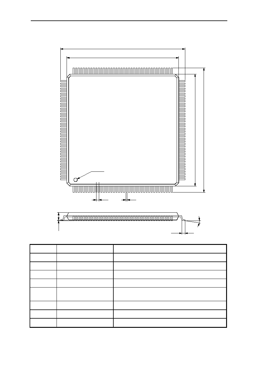
7-10 CHAPTER 7
7.4 Package-Dimensions
b
D
D
1
E
1
Index
A
1
A
2
L
E
P
Figure 7.4: GMS30C2232, GMS30C2216 Package-Outline
Symbol
Term
Definition
A1
Standoff height
Height from ground plane to bottom edge of package
A2
Package height
Height of package itself
E, D
Overall length & width
Length and width including leads
D1, E1
Package length & width
Length and width of package
L
Length of flat lead
section
Length of flat lead section
P
Lead pitch
Lead pitch
b
Lead width
Width of a lead
Lead angle
Angle of lead versus seating plane
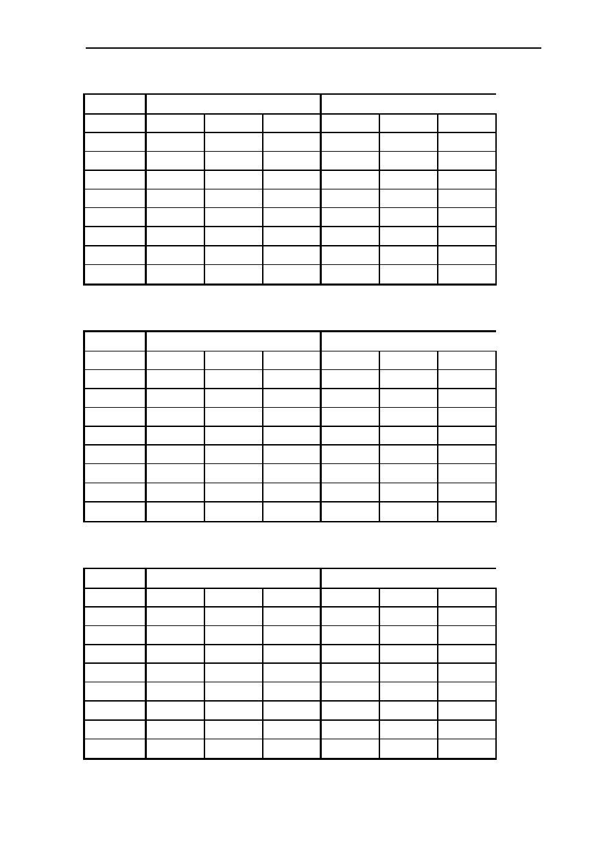
MECHANICAL DATA 7-11
GMS30C2232, 160-Pin MQFP-Package
Symbol
Dimensions in Millimeters
Dimensions in Inches
Min.
Nom.
Max.
Min.
Nom.
Max
A1
0.25
0.36
0.47
(0.010)
(0.014)
(0.018)
A2
3.20
3.40
3.60
(0.126)
(0.134)
(0.142)
E, D
31.20
31.90
32.15
(1.228)
(1.256)
(1.266)
E1, D1
27.90
28.00
28.10
(1.098)
(1.102)
(1.106)
L
0.63
0.88
1.03
(0.025)
(0.035)
(0.041)
P
0.65
(0.0256)
b
0.22
0.29
0.38
(0.009)
(0.012)
(0.015)
0°
7°
(0°)
(7°)
GMS30C2232, 144-Pin TQFP-Package
Symbol
Dimensions in Millimeters
Dimensions in Inches
Min.
Nom.
Max.
Min.
Nom.
Max
A1
0.05
0.10
0.15
(0.002)
(0.004)
(0.006)
A2
1.35
1.40
1.45
(0.053)
(0.055)
(0.057)
E, D
21.80
22.00
22.20
(0.858)
(0.866)
(0.874)
E1, D1
19.90
20.00
20.10
(0.783)
(0.787)
(0.791)
L
0.45
0.60
0.75
(0.018)
(0.024)
(0.030)
P
0.50
(0.0197)
b
0.17
0.22
0.27
(0.007)
(0.009)
(0.011)
0°
7°
(0°)
(7°)
GMS30C2216, 100-Pin TQFP-Package
Symbol
Dimensions in Millimeters
Dimensions in Inches
Min.
Nom.
Max.
Min.
Nom.
Max
A1
0.05
0.10
0.15
(0.002)
(0.004)
(0.006)
A2
1.35
1.40
1.45
(0.053)
(0.055)
(0.057)
E, D
15.80
16.00
16.20
(0.622)
(0.630)
(0.638)
E1, D1
13.90
14.00
14.10
(0.547)
(0.551)
(0.555)
L
0.45
0.60
0.75
(0.018)
(0.024)
(0.030)
P
0.50
(0.0197)
b
0.17
0.22
0.27
(0.007)
(0.009)
(0.011)
0°
7°
(0°)
(7°)


Appendix A. Instruction Set Details A-1
Appendix. Instruction Set Details
This appendix provides a detailed description of the operation of each GMS30C2216/32
RISC/DSP instruction. The instructions are listed in alphabet order.
The exceptions that may occur due to the execution of each instruction are listed after the
description of each instruction. The description of the immediate causes and manner of
handling exceptions is omitted from the instruction description in this chapter. Refer to
chapter 4 for detailed description of exceptions and handling.
Instruction Classes
GMS30C2216/32 RISC/DSP instructions are divided into 7 classes
1. Memory Instruction: Load data form memory in a register or store data from a register
to memory. I/O devices are also addressed by memory instructions.
2. Move Instruction: Source operand or the immediate operand is copied to the
destination register.
3. Computational Instruction: Perform arithmetic, logical, shift and rotate operations on
values in registers.
4. Branch and Delayed Branch Instruction: When the branch condition is met, place the
branch address PC+rel in the program counter PC and clear the cache-mode flag M.
5. Extended DSP Instruction: The extended DSP functions use the on-chip multiply-
accumulate unit.
6. Software Instruction: Cause a branch to the subprogram associated with each Software
instruction.
7. Special Instruction: Call, Trap, Frame, Return and Fetch instruction
Instruction Notation
Instruction notation is same as the notation of using chapter 2 and 3. (see section 2.1
Instruction Notation)

A-2 Appendix A. Instruction Set Details
ADD
ADD
Format:
RR format
Rd-code
Rs-code
OP-code
0010 10
d
s
15
10
9
8
7
4 3
0
s = 0: Rs-code encoded G0..G15 for Rs
s = 1: Rs-code encoded L0..L15 for Rs
d = 0: Rd-code encoded G0..G15 for Rd
d = 1: Rd-code encoded L0..L15 for Rd
Notation:
ADD Rd, Rs
ADD Rd, C (when SR is denoted as a Rs)
Description:
The source operand (Rs) is added to the destination operand (Rd), the result is placed in the
destination register (Rd) and the condition flag are set or cleared accordingly.
Both operands and the result are interpreted as either all signed or all unsigned integers.
When the SR is denoted as a source operand, carry flag C is added instead of the SR.
Operation:
When Rs is not SR
Rd := Rd + Rs;
Z := Rd = 0;
N := Rd(31);
V := overflow;
C := carry;
When Rs is SR
Rd := Rd + C;
Z := Rd = 0;
N := Rd(31);
V := overflow;
C := carry;
Exceptions:
None.

Appendix A. Instruction Set Details A-3
ADD with carry
ADDC
Format:
RR format
Rd-code
Rs-code
OP-code
0101 00
d
s
15
10
9
8
7
4 3
0
s = 0: Rs-code encoded G0..G15 for Rs
s = 1: Rs-code encoded L0..L15 for Rs
d = 0: Rd-code encoded G0..G15 for Rd
d = 1: Rd-code encoded L0..L15 for Rd
Notation:
ADDC Rd, Rs
ADDC Rd, C (when SR is denoted as a Rs)
Description:
The source operand (Rs) + C is added to the destination operand (Rd), the result is placed
in the destination register (Rd) and the condition flag are set or cleared accordingly.
Both operands and the result are interpreted as either all signed or all unsigned integers.
When the SR is denoted as a source operand, carry flag C is added instead of the SR.
Operation:
When Rs is not SR
Rd := Rd + Rs + C;
Z := Z and (Rd=0);
N := Rd(31);
V := overflow;
C := carry;
When Rs is SR
Rd := Rd + C;
Z := Z and (Rd=0);
N := Rd(31);
V := overflow;
C := carry;
Exceptions:
None.
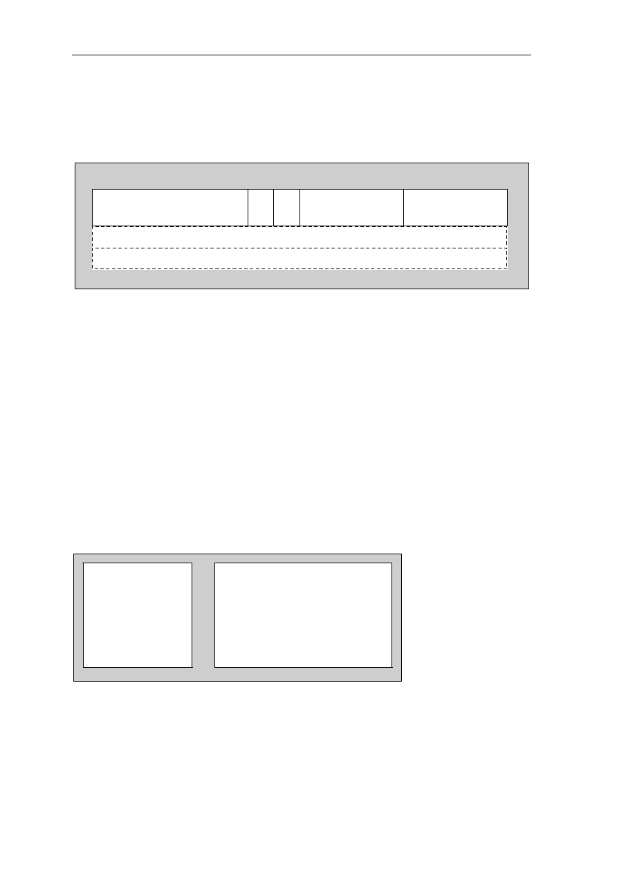
A-4 Appendix A. Instruction Set Details
ADD Immediate
ADDI
Format:
Rimm format
d = 0: Rd-code encoded G0..G15 for Rd
d = 1: Rd-code encoded L0..L15 for Rd
n: bit 8 // bit 3..0 encode n = 0..31, see Table 2.3 Encoding of Immediate Values
Rd-code
n
OP-code
0100 10
d
n
15
10
9
8
7
4 3
0
imm1
imm2
Notation:
ADDI Rd, imm
ADDI Rd, CZ (when n = 0 )
Description:
The immediate operand (imm) is added to the destination operand (Rd), the result is placed
in the destination register (Rd) and the condition flag are set or cleared accordingly.
Both operands and the result are interpreted as either all signed or all unsigned integers.
When the immediate value n = 0, C is only added to the destination operand if Z = 0 or
Rd(0) is one (round to even).
Operation:
When n is not zero
Rd := Rd + imm;
Z := Rd = 0;
N := Rd(31);
V := overflow;
C := carry;
When n is zero
Rd := Rd + (C and (Z=0 or Rd(0)));
Z := Rd = 0
N := Rd(31);
V := overflow;
C := carry;
Exceptions:
None.

Appendix A. Instruction Set Details A-5
Signed ADD with trap
ADDS
Format:
RR format
Rd-code
Rs-code
OP-code
0010 11
d
s
15
10
9
8
7
4 3
0
s = 0: Rs-code encoded G0..G15 for Rs
s = 1: Rs-code encoded L0..L15 for Rs
d = 0: Rd-code encoded G0..G15 for Rd
d = 1: Rd-code encoded L0..L15 for Rd
Notation:
ADDS Rd, Rs
ADDS Rd, C (when SR is denoted as a Rs)
Description:
The source operand (Rs) is added to the destination operand (Rd), the result is placed in the
destination register (Rd) and the condition flag are set or cleared accordingly.
Both operands and the result are signed integers and a trap to Range Error occurs at
overflow.
When the SR is denoted as a source operand, carry flag C is added instead of the SR.
Operation:
When Rs is not SR
Rd := Rd + Rs;
Z := Rd = 0;
N := Rd(31);
V := overflow;
if overflow then
trap -> Range Error
When Rs is SR
Rd := Rd + C;
Z := Rd = 0;
N := Rd(31);
V := overflow;
if overflow then
trap -> Range Error
Exceptions:
Overflow exception (trap to Range Error).
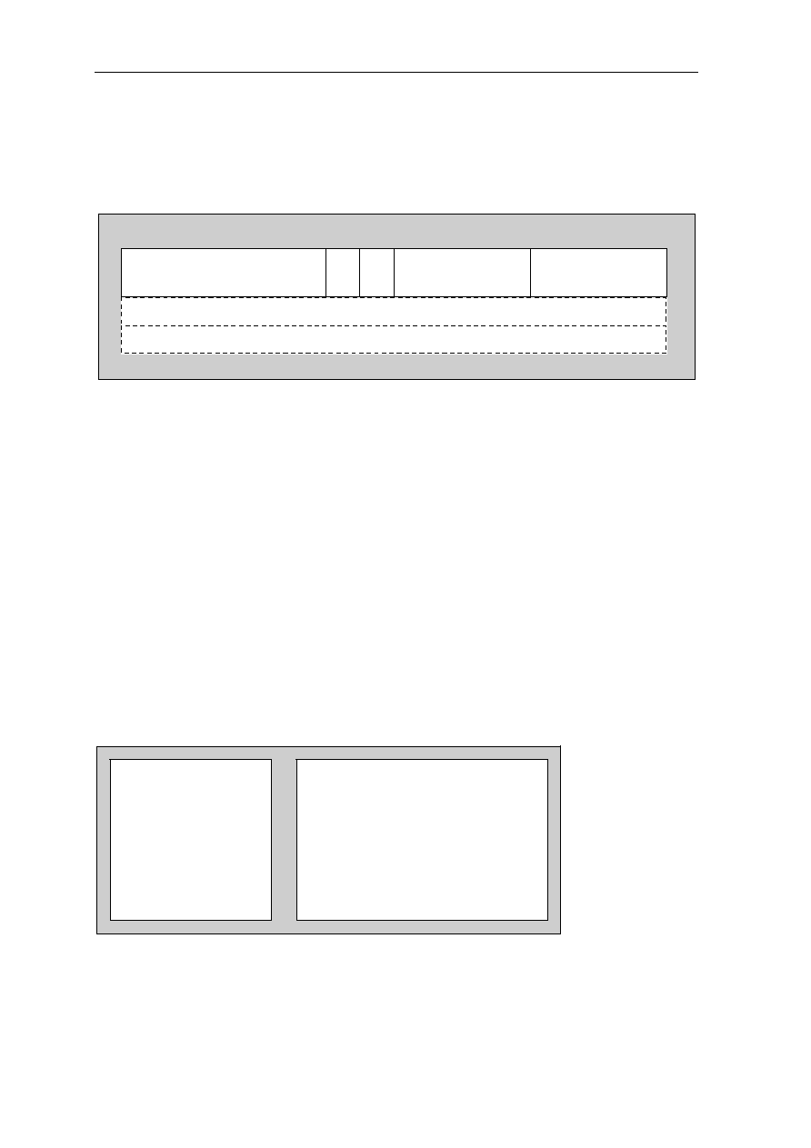
A-6 Appendix A. Instruction Set Details
Signed ADD Immediate with trap
ADDSI
Format:
Rimm format
d = 0: Rd-code encoded G0..G15 for Rd
d = 1: Rd-code encoded L0..L15 for Rd
n: bit 8 // bit 3..0 encode n = 0..31, see Table 2.3 Encoding of Immediate Values
Rd-code
n
OP-code
0110 11
d
n
15
10
9
8
7
4 3
0
imm1
imm2
Notation:
ADDSI Rd, imm
ADDSI Rd, CZ (when n = 0 )
Description:
The immediate operand (imm) is added to the destination operand (Rd), the result is placed
in the destination register (Rd) and the condition flag are set or cleared accordingly.
Both operands and the result are signed integers and a trap to Range Error occurs at
overflow.
When the immediate value n = 0, C is only added to the destination operand if Z = 0 or
Rd(0) is one (round to even).
Operation:
When Rs is not SR
Rd := Rd + imm;
Z := Rd = 0;
N := Rd(31);
V := overflow;
if overflow then
trap -> Range Error
When Rs is SR
Rd := Rd + (C and (Z=0 or Rd(0)));
Z := Rd = 0;
N := Rd(31);
V := overflow;
if overflow then
trap -> Range Error
Exceptions:
Overflow exception (trap to Range Error)

Appendix A. Instruction Set Details A-7
AND
AND
Format:
RR format
Rd-code
Rs-code
OP-code
0101 01
d
s
15
10
9
8
7
4 3
0
s = 0: Rs-code encoded G0..G15 for Rs
s = 1: Rs-code encoded L0..L15 for Rs
d = 0: Rd-code encoded G0..G15 for Rd
d = 1: Rd-code encoded L0..L15 for Rd
Notation:
AND Rd, Rs
Description:
The result of a bitwise logical AND of the source operand (Rs) and the destination operand
(Rd) is placed in the destination register (Rd) and the Z flag is set or cleared accordingly.
Operation:
Rd := Rd and Rs;
Z := Rd = 0;
Exceptions:
None.

A-8 Appendix A. Instruction Set Details
AND with source used inverted
ANDN
Format:
RR format
Rd-code
Rs-code
OP-code
0011 01
d
s
15
10
9
8
7
4 3
0
s = 0: Rs-code encoded G0..G15 for Rs
s = 1: Rs-code encoded L0..L15 for Rs
d = 0: Rd-code encoded G0..G15 for Rd
d = 1: Rd-code encoded L0..L15 for Rd
Notation:
ANDN Rd, Rs
Description:
The result of a bitwise logical AND not (ANDN) of the source operand (Rs) and the
destination operand (Rd) is placed in the destination register (Rd) and the Z flag is set or
cleared accordingly. The source operand is used inverted (itself remaining unchanged).
Operation:
Rd := Rd and not Rs;
Z := Rd = 0;
Exceptions:
None.

Appendix A. Instruction Set Details A-9
AND with imm used inverted
ANDNI
Format:
Rimm format
d = 0: Rd-code encoded G0..G15 for Rd
d = 1: Rd-code encoded L0..L15 for Rd
n: bit 8 // bit 3..0 encode n = 0..31, see Table 2.3 Encoding of Immediate Values
Rd-code
n
OP-code
0111 01
d
n
15
10
9
8
7
4 3
0
imm1
imm2
Notation:
ANDNI Rd, imm
Description:
The result of a bitwise logical AND not (ANDN) of the source operand (Rs) and the
immediate operand (Rd) is placed in the destination register (Rd) and the Z flag is set or
cleared accordingly. The immediate operand is used inverted (itself remaining unchanged).
Operation:
Rd := Rd and not imm;
Z := Rd = 0;
Exceptions:
None.

A-10 Appendix A. Instruction Set Details
Branch on Carry
BC
Format:
PCrel format
low-rel
OP-code
1111 0100
15
6
8
7
0
S: sign bit of rel
rel = 25 S // low-rel // 0
range -128 ~ 126
0
S
Notation:
BC rel
Description:
If the carry flag C is set (C = 1), place the branch address PC + rel (relative of the first byte
after the Branch instruction) in the program counter PC and clear the cache-mode flag M;
all condition flags remain unchanged. Then instruction execution proceeds at the branch
address placed in the PC
When the branch condition is not met, the M flag and the condition flags remain
unchanged and instruction execution proceeds sequentially.
Note: rel is signed to allow forward or backward branches.
Operation:
If C = 1 then
PC := PC + rel
M := 0
Exceptions:
None.

Appendix A. Instruction Set Details A-11
Branch on Equal
BE
Format:
PCrel format
low-rel
OP-code
1111 0010
15
6
8
7
0
S: sign bit of rel
rel = 25 S // low-rel // 0
range -128 ~ 126
0
S
Notation:
BE rel
Description:
If the zero flag is set (Z = 1), place the branch address PC + rel (relative of the first byte
after the Branch instruction) in the program counter PC and clear the cache-mode flag M;
all condition flags remain unchanged. Then instruction execution proceeds at the branch
address placed in the PC
When the branch condition is not met, the M flag and the condition flags remain
unchanged and instruction execution proceeds sequentially.
Note: rel is signed to allow forward or backward branches.
Operation:
If Z = 1 then
PC := PC + rel
M := 0
Exceptions:
None.

A-12 Appendix A. Instruction Set Details
Branch on Greater or Equal
BGE
Format:
PCrel format
low-rel
OP-code
1111 1001
15
6
8
7
0
S: sign bit of rel
rel = 25 S // low-rel // 0
range -128 ~ 126
0
S
Notation:
BGE rel
Description:
If the negative flag N is cleared (N = 0, non-negative), place the branch address PC + rel
(relative of the first byte after the Branch instruction) in the program counter PC and clear
the cache-mode flag M; all condition flags remain unchanged. Then instruction execution
proceeds at the branch address placed in the PC
When the branch condition is not met, the M flag and the condition flags remain
unchanged and instruction execution proceeds sequentially.
Note: rel is signed to allow forward or backward branches.
Operation:
If N = 0 then
PC := PC + rel
M := 0
Exceptions:
None.

Appendix A. Instruction Set Details A-13
Branch on Greater Than
BGT
Format:
PCrel format
low-rel
OP-code
1111 1011
15
6
8
7
0
S: sign bit of rel
rel = 25 S // low-rel // 0
range -128 ~ 126
0
S
Notation:
BGT rel
Description:
If the negative flag N and the zero flag Z are cleared (N = 0 and Z = 0), place the branch
address PC + rel (relative of the first byte after the Branch instruction) in the program
counter PC and clear the cache-mode flag M; all condition flags remain unchanged. Then
instruction execution proceeds at the branch address placed in the PC
When the branch condition is not met, the M flag and the condition flags remain
unchanged and instruction execution proceeds sequentially.
Note: rel is signed to allow forward or backward branches.
Operation:
If N=0 and Z=0 then
PC := PC + rel
M := 0
Exceptions:
None.

A-14 Appendix A. Instruction Set Details
Branch on Higher or Equal
BHE
Format:
PCrel format
low-rel
OP-code
1111 0101
15
6
8
7
0
S: sign bit of rel
rel = 25 S // low-rel // 0
range -128 ~ 126
0
S
Notation:
BHE rel
Description:
If the carry flag C is cleared (C = 0), place the branch address PC + rel (relative of the first
byte after the Branch instruction) in the program counter PC and clear the cache-mode flag
M; all condition flags remain unchanged. Then instruction execution proceeds at the
branch address placed in the PC
When the branch condition is not met, the M flag and the condition flags remain
unchanged and instruction execution proceeds sequentially.
Note: rel is signed to allow forward or backward branches.
Operation:
If C = 0 then
PC := PC + rel
M := 0
Exceptions:
None.

Appendix A. Instruction Set Details A-15
Branch on Higher Than
BHT
Format:
PCrel format
low-rel
OP-code
1111 0111
15
6
8
7
0
S: sign bit of rel
rel = 25 S // low-rel // 0
range -128 ~ 126
0
S
Notation:
BHE rel
Description:
If the carry flag C and the zero flag Z are cleared (C = 0 and Z = 0), place the branch
address PC + rel (relative of the first byte after the Branch instruction) in the program
counter PC and clear the cache-mode flag M; all condition flags remain unchanged. Then
instruction execution proceeds at the branch address placed in the PC
When the branch condition is not met, the M flag and the condition flags remain
unchanged and instruction execution proceeds sequentially.
Note: rel is signed to allow forward or backward branches.
Operation:
If C=0 and Z=0 then
PC := PC + rel
M := 0
Exceptions:
None.

A-16 Appendix A. Instruction Set Details
Branch on Less or Equal
BLE
Format:
PCrel format
low-rel
OP-code
1111 1010
15
6
8
7
0
S: sign bit of rel
rel = 25 S // low-rel // 0
range -128 ~ 126
0
S
Notation:
BLE rel
Description:
If the negative flag N is set or the zero flag Z is set (N = 1 or Z = 1), place the branch
address PC + rel (relative of the first byte after the Branch instruction) in the program
counter PC and clear the cache-mode flag M; all condition flags remain unchanged. Then
instruction execution proceeds at the branch address placed in the PC
When the branch condition is not met, the M flag and the condition flags remain
unchanged and instruction execution proceeds sequentially.
Note: rel is signed to allow forward or backward branches.
Operation:
If N=1 or Z=1 then
PC := PC + rel
M := 0
Exceptions:
None.

Appendix A. Instruction Set Details A-17
Branch on Less Than
BLT
Format:
PCrel format
low-rel
OP-code
1111 1000
15
6
8
7
0
S: sign bit of rel
rel = 25 S // low-rel // 0
range -128 ~ 126
0
S
Notation:
BLT rel
Description:
If the negative flag N is set (N = 1), place the branch address PC + rel (relative of the first
byte after the Branch instruction) in the program counter PC and clear the cache-mode flag
M; all condition flags remain unchanged. Then instruction execution proceeds at the
branch address placed in the PC
When the branch condition is not met, the M flag and the condition flags remain
unchanged and instruction execution proceeds sequentially.
Note: rel is signed to allow forward or backward branches.
Operation:
If N = 1 then
PC := PC + rel
M := 0
Exceptions:
None.

A-18 Appendix A. Instruction Set Details
Branch on Negative
BN
Format:
PCrel format
low-rel
OP-code
1111 1000
15
6
8
7
0
S: sign bit of rel
rel = 25 S // low-rel // 0
range -128 ~ 126
0
S
Notation:
BN rel
Description:
If the negative flag N is set (N = 1), place the branch address PC + rel (relative of the first
byte after the Branch instruction) in the program counter PC and clear the cache-mode flag
M; all condition flags remain unchanged. Then instruction execution proceeds at the
branch address placed in the PC
When the branch condition is not met, the M flag and the condition flags remain
unchanged and instruction execution proceeds sequentially.
Note: rel is signed to allow forward or backward branches.
Operation:
If N = 1 then
PC := PC + rel
M := 0
Exceptions:
None.

Appendix A. Instruction Set Details A-19
Branch on No Carry
BNC
Format:
PCrel format
low-rel
OP-code
1111 0101
15
6
8
7
0
S: sign bit of rel
rel = 25 S // low-rel // 0
range -128 ~ 126
0
S
Notation:
BNC rel
Description:
If the carry flag C is cleared (C = 0), place the branch address PC + rel (relative of the first
byte after the Branch instruction) in the program counter PC and clear the cache-mode flag
M; all condition flags remain unchanged. Then instruction execution proceeds at the
branch address placed in the PC
When the branch condition is not met, the M flag and the condition flags remain
unchanged and instruction execution proceeds sequentially.
Note: rel is signed to allow forward or backward branches.
Operation:
If C = 0 then
PC := PC + rel
M := 0
Exceptions:
None.

A-20 Appendix A. Instruction Set Details
Branch on Not Equal
BNE
Format:
PCrel format
low-rel
OP-code
1111 0011
15
6
8
7
0
S: sign bit of rel
rel = 25 S // low-rel // 0
range -128 ~ 126
0
S
Notation:
BNE rel
Description:
If the zero flag Z is cleared (Z = 0), place the branch address PC + rel (relative of the first
byte after the Branch instruction) in the program counter PC and clear the cache-mode flag
M; all condition flags remain unchanged. Then instruction execution proceeds at the
branch address placed in the PC
When the branch condition is not met, the M flag and the condition flags remain
unchanged and instruction execution proceeds sequentially.
Note: rel is signed to allow forward or backward branches.
Operation:
If Z = 0 then
PC := PC + rel
M := 0
Exceptions:
None.

Appendix A. Instruction Set Details A-21
Branch on Non-Negative
BNN
Format:
PCrel format
low-rel
OP-code
1111 1001
15
6
8
7
0
S: sign bit of rel
rel = 25 S // low-rel // 0
range -128 ~ 126
0
S
Notation:
BNN rel
Description:
If the negative flag N is cleared (N = 0, non-negative), place the branch address PC + rel
(relative of the first byte after the Branch instruction) in the program counter PC and clear
the cache-mode flag M; all condition flags remain unchanged. Then instruction execution
proceeds at the branch address placed in the PC
When the branch condition is not met, the M flag and the condition flags remain
unchanged and instruction execution proceeds sequentially.
Note: rel is signed to allow forward or backward branches.
Operation:
If N = 0 then
PC := PC + rel
M := 0
Exceptions:
None.

A-22 Appendix A. Instruction Set Details
Branch on Not Overflow
BNV
Format:
PCrel format
low-rel
OP-code
1111 0001
15
6
8
7
0
S: sign bit of rel
rel = 25 S // low-rel // 0
range -128 ~ 126
0
S
Notation:
BNV rel
Description:
If the overflow flag V is cleared (V = 0), place the branch address PC + rel (relative of the
first byte after the Branch instruction) in the program counter PC and clear the cache-mode
flag M; all condition flags remain unchanged. Then instruction execution proceeds at the
branch address placed in the PC
When the branch condition is not met, the M flag and the condition flags remain
unchanged and instruction execution proceeds sequentially.
Note: rel is signed to allow forward or backward branches.
Operation:
If V = 0 then
PC := PC + rel
M := 0
Exceptions:
None.

Appendix A. Instruction Set Details A-23
Branch on None-Zero
BNZ
Format:
PCrel format
low-rel
OP-code
1111 0011
15
6
8
7
0
S: sign bit of rel
rel = 25 S // low-rel // 0
range -128 ~ 126
0
S
Notation:
BNZ rel
Description:
If the zero flag Z is cleared (Z = 0), place the branch address PC + rel (relative of the first
byte after the Branch instruction) in the program counter PC and clear the cache-mode flag
M; all condition flags remain unchanged. Then instruction execution proceeds at the
branch address placed in the PC
When the branch condition is not met, the M flag and the condition flags remain
unchanged and instruction execution proceeds sequentially.
Note: rel is signed to allow forward or backward branches.
Operation:
If Z = 0 then
PC := PC + rel
M := 0
Exceptions:
None.

A-24 Appendix A. Instruction Set Details
Branch on Smaller or Equal
BSE
Format:
PCrel format
low-rel
OP-code
1111 0110
15
6
8
7
0
S: sign bit of rel
rel = 25 S // low-rel // 0
range -128 ~ 126
0
S
Notation:
BSE rel
Description:
If the carry flag C is set (C = 1) or the zero flag is set (Z = 1), place the branch address PC
+ rel (relative of the first byte after the Branch instruction) in the program counter PC and
clear the cache-mode flag M; all condition flags remain unchanged. Then instruction
execution proceeds at the branch address placed in the PC
When the branch condition is not met, the M flag and the condition flags remain
unchanged and instruction execution proceeds sequentially.
Note: rel is signed to allow forward or backward branches.
Operation:
If C=1 or Z=1 then
PC := PC + rel
M := 0
Exceptions:
None.

Appendix A. Instruction Set Details A-25
Branch
BR
Format:
PCrel format
low-rel
OP-code
1111 1100
15
6
8
7
0
S: sign bit of rel
rel = 25 S // low-rel // 0
range -128 ~ 126
0
S
Notation:
BR rel
Description:
Place the branch address PC + rel (relative of the first byte after the Branch instruction) in
the program counter PC and clear the cache-mode flag M; all condition flags remain
unchanged. Then instruction execution proceeds at the branch address placed in the PC
Note: rel is signed to allow forward or backward branches.
Operation:
PC := PC + rel
M := 0
Exceptions:
None.

A-26 Appendix A. Instruction Set Details
Branch on Overflow
BV
Format:
PCrel format
low-rel
OP-code
1111 0000
15
6
8
7
0
S: sign bit of rel
rel = 25 S // low-rel // 0
range -128 ~ 126
0
S
Notation:
BV rel
Description:
If the overflow flag V is set (V = 1), place the branch address PC + rel (relative of the first
byte after the Branch instruction) in the program counter PC and clear the cache-mode flag
M; all condition flags remain unchanged. Then instruction execution proceeds at the
branch address placed in the PC
When the branch condition is not met, the M flag and the condition flags remain
unchanged and instruction execution proceeds sequentially.
Note: rel is signed to allow forward or backward branches.
Operation:
If V = 1 then
PC := PC + rel
M := 0
Exceptions:
None.

Appendix A. Instruction Set Details A-27
Branch on Zero
BZ
Format:
PCrel format
low-rel
OP-code
1111 0010
15
6
8
7
0
S: sign bit of rel
rel = 25 S // low-rel // 0
range -128 ~ 126
0
S
Notation:
BZ rel
Description:
If the zero flag is set (Z = 1), place the branch address PC + rel (relative of the first byte
after the Branch instruction) in the program counter PC and clear the cache-mode flag M;
all condition flags remain unchanged. Then instruction execution proceeds at the branch
address placed in the PC
When the branch condition is not met, the M flag and the condition flags remain
unchanged and instruction execution proceeds sequentially.
Note: rel is signed to allow forward or backward branches.
Operation:
If Z = 1 then
PC := PC + rel
M := 0
Exceptions:
None.
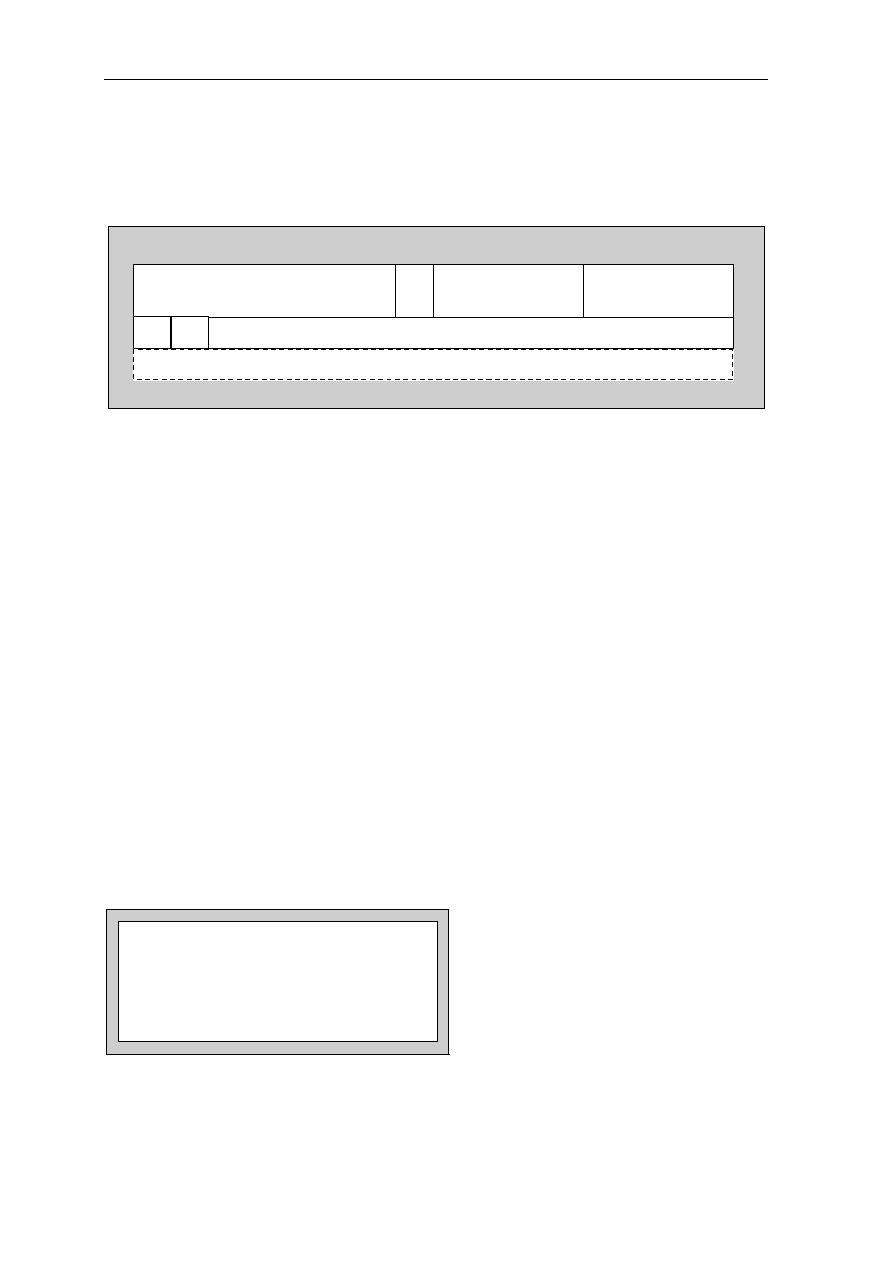
A-28 Appendix A. Instruction Set Details
Call
CALL
Format:
LRconst format
s = 0: Rs-code encoded G0..G15 for Rs
s = 1: Rs-code encoded L0..L15 for Rs, Ld-code encodes L0..L15 for Ld
S: Sign bit of const
e = 0: const = 18S // const1, range -16,384 ~ 16,383
e = 1: const = 2S // const1 // const2, range -1,073,741,824 ~ 1,073,741,823
Ld-code
Rs-code
OP-code
1110111
s
15
9
8
7
4 3
0
imm1
imm2
const1
const2
e
S
Notation:
CALL Ld, Rs, const
CALL Ld, 0, const (when Rs denotes SR)
Description:
The Call instruction causes a branch to a subprogram.
The branch address Rs + const, or const alone if Rs denotes the SR, is placed in the
program counter PC. The old PC containing the return address is saved in Ld; the old
supervisor-state flag S is also saved in bit zero of Ld. The old status register SR is saved in
Ldf, the saved instruction-length code ILC contains the length (2 or 3) of the Call
instruction. Then the frame pointer FP is incremented by the value of the Ld-code and the
frame length FL is set to six, thus creating a new stack frame.
The cache-mode flag M is cleared. All condition flags remain unchanged. Then instruction
execution proceeds at the branch address placed in the PC.
Operation:
If Rs denotes not SR then PC := Rs +const
else PC := const
Ld := old PC(31..1) // old S;
Ldf := old SR;
FP := Fo + Ld code; (Ld-cod 0 is treated as 16)
FL := 6; M:= 0;
Exceptions:
None.

Appendix A. Instruction Set Details A-29
Check
CHK
Format:
RR format
Rd-code
Rs-code
OP-code
0000 00
d
s
15
10
9
8
7
4 3
0
s = 0: Rs-code encoded G0..G15 for Rs
s = 1: Rs-code encoded L0..L15 for Rs
d = 0: Rd-code encoded G0..G15 for Rd
d = 1: Rd-code encoded L0..L15 for Rd
Notation:
CHK Rd, Rs
Description:
A destination operand is checked and a trap to a Range Error occurs if the destination
operand is higher than the source operand.
All registers and all condition flags remain unchanged. All operands are interpreted as
unsigned integers.
When Rs denotes the PC, CHK trap if Rd > PC. Thus, CHK PC, PC always traps. Since
CHK PC, PC is encoded as 16 zeros, an erroneous jump into a string of zeros causes a trap
to Range Error, thus trapping some address errors.
Operation:
If Rs does not denote SR and Rd > Rs then
trap -> Range Error
Exceptions:
Range Error.

A-30 Appendix A. Instruction Set Details
Check Zero
CHKZ
Format:
RR format
Rd-code
Rs-code
OP-code
0000 00
d
s
15
10
9
8
7
4 3
0
s = 0: Rs-code encoded G0..G15 for Rs
s = 1: Rs-code encoded L0..L15 for Rs
d = 0: Rd-code encoded G0..G15 for Rd
d = 1: Rd-code encoded L0..L15 for Rd
Notation:
CHK Rd, 0
Description:
A destination operand is checked and a trap to a Range Error occurs if the destination
operand is zero.
All registers and all condition flags remain unchanged. All operands are interpreted as
unsigned integers.
CHKZ shares its basic OP-code with CHK, it is differentiated by denoting the SR as source
operand.
CHKZ may be used to trap on uninitialized pointers with the value zero.
Operation:
If Rs denotes SR and Rd = 0 then
trap -> Range Error
Exceptions:
Range Error.

Appendix A. Instruction Set Details A-31
Compare with Source Operand
CMP
Format:
RR format
Rd-code
Rs-code
OP-code
0010 00
d
s
15
10
9
8
7
4 3
0
s = 0: Rs-code encoded G0..G15 for Rs
s = 1: Rs-code encoded L0..L15 for Rs
d = 0: Rd-code encoded G0..G15 for Rd
d = 1: Rd-code encoded L0..L15 for Rd
Notation:
CMP Rd, Rs
CMP Rd, C (when Rs denotes SR)
Description:
Two operands are compared by subtracting the source operand from the destination
operand. The condition flags are set or cleared according to the result; the result itself is
not retained. Note that the N flag indicates the correct compare result even in the case of an
overflow.
All operands and the result are interpreted as either all signed or all unsigned integers.
When the SR is denoted as a source operand at CMP, C is subtracted instead of SR.
Operation:
When Rs is not SR
result := Rd - Rs;
Z := Rd = Rs;
N := Rd < Rs signed;
V := overflow;
C := Rd < RS unsigned;
When Rs is SR
result := Rd - C;
Z := Rd = C;
N := Rd < C signed;
V := overflow;
C := Rd < C unsigned;
Exceptions:
None

A-32 Appendix A. Instruction Set Details
Compare Bit
CMPB
Format:
RR format
Rd-code
Rs-code
OP-code
0011 00
d
s
15
10
9
8
7
4 3
0
s = 0: Rs-code encoded G0..G15 for Rs
s = 1: Rs-code encoded L0..L15 for Rs
d = 0: Rd-code encoded G0..G15 for Rd
d = 1: Rd-code encoded L0..L15 for Rd
Notation:
CMPB Rd, Rs
Description:
The result of a bitwise logical AND of the source operand and the destination operand is
used to set or clear the Z flag accordingly; the result itself is not retained.
All operands and the result are interpreted as bit-string of 32 bits each.
Operation:
Z := (Rd and Rs) = 0;
Exceptions:
None
Appendix A. Instruction Set Details A-33
Compare Bit with Immediate
CMPBI
Format:
Rimm format
d = 0: Rd-code encoded G0..G15 for Rd
d = 0: Rd-code encoded L0..L15 for Rd
n: bit 8 // bit 3..0 encode n = 0..31, see Table 2.3 Encoding of Immediate Values
Rd-code
n
OP-code
0111 00
d
n
15
10
9
8
7
4 3
0
imm1
imm2
Notation:
CMPBI Rd, imm
CMPBI Rd, ANYBZ (when n = 0)
Description:
The result of a bitwise logical AND of the immediate operand and the destination operand
is used to set or clear the Z flag accordingly; the result itself is not retained.
All operands and the result are interpreted as bit-string of 32 bits each.
A special case of CMPBI differentiated by n = 0, if any byte of the destination operand is
zero then the zero flag Z is set (Z = 1).
Operation:
If n is not zero then
Z := (Rd and imm);
else
Z := Rd(31..24) = 0 or Rd(23..16) = 0 or
Rd(15..8) = 0 or Rd(7..0) = 0
Exceptions:
None
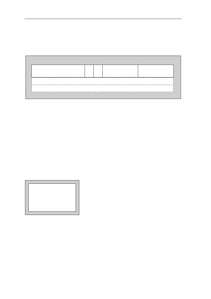
A-34 Appendix A. Instruction Set Details
Compare with Immediate
CMPI
Format:
Rimm format
d = 0: Rd-code encoded G0..G15 for Rd
d = 1: Rd-code encoded L0..L15 for Rd
n: bit 8 // bit 3..0 encode n = 0..31, see Table 2.3 Encoding of Immediate Values
Rd-code
n
OP-code
0110 00
d
n
15
10
9
8
7
4 3
0
imm1
imm2
Notation:
CMPI Rd, imm
Description:
Two operands are compared by subtracting the source operand from the destination
operand. The condition flags are set or cleared according to the result; the result itself is
not retained. Note that the N flag indicates the correct compare result even in the case of an
overflow.
All operands and the result are interpreted as either all signed or all unsigned integers.
Operation:
result := Rd - imm;
Z := Rd = imm;
N := Rd < imm signed;
V := overflow;
C := Rd < imm unsigned;
Exceptions:
None

Appendix A. Instruction Set Details A-35
Divide with Non-Negative Signed
DIVS
Format:
RR format
Rd-code
Rs-code
OP-code
0000 11
d
s
15
10
9
8
7
4 3
0
s = 0: Rs-code encoded G0..G15 for Rs
s = 1: Rs-code encoded L0..L15 for Rs
d = 0: Rd-code encoded G0..G15 for Rd
d = 1: Rd-code encoded L0..L15 for Rd
Notation:
DIVS Rd, Rs
Description:
The double-word destination operand (dividend) is divided by the single-word source
operand (divisor), the quotient is placed in the low-order destination register (Rdf), the
remainder is placed in the high-order destination register (Rd) and the condition flags are
set or cleared according to the quotient.
A trap to Range Error occurs if the divisor is zero or the value of the quotient exceeds the
integer value range (quotient overflow). The result (in Rd//Rdf) is then undefined. A trap to
Range Error also occurs and the result is undefined if the dividend is negative.
The dividend is a non-negative signed double-word integer, the devisor, the quotient and
the remainder are signed integers; a non-zero remainder has the sign of the dividend.
The result is undefined if Rs denotes the same register as Rd or Rdf or if the PC or the SR
is denoted.
Operation:
If Rs = 0 or quotient overflow or Rd(31) = 1 then
Rd//Rdf := undefined;
Z := undefined;, N := undefined;,
V :=1 trap -> Range Error
else
remainder Rd, quotient Rdf := (Rd//Rdf) / Rs;
Z := Rdf = 0
N := Rd(31),
V:= 0;
Exceptions:
Quotient Overflow (Trap to a Range Error)
Division by Zero (Trap to a Range Error)
Dividend is Negative (Trap to a Range Error)

A-36 Appendix A. Instruction Set Details
Divide with Unsigned
DIVU
Format:
RR format
Rd-code
Rs-code
OP-code
0000 10
d
s
15
10
9
8
7
4 3
0
s = 0: Rs-code encoded G0..G15 for Rs
s = 1: Rs-code encoded L0..L15 for Rs
d = 0: Rd-code encoded G0..G15 for Rd
d = 1: Rd-code encoded L0..L15 for Rd
Notation:
DIVU Rd, Rs
Description:
The double-word destination operand (dividend) is divided by the single-word source
operand (divisor), the quotient is placed in the low-order destination register (Rdf), the
remainder is placed in the high-order destination register (Rd) and the condition flags are
set or cleared according to the quotient.
A trap to Range Error occurs if the divisor is zero or the value of the quotient exceeds the
integer value range (quotient overflow). The result (in Rd//Rdf) is then undefined.
The dividend is an unsigned double-word integer, the devisor, the quotient and the
remainder are unsigned integers
The result is undefined if Rs denotes the same register as Rd or Rdf or if the PC or the SR
is denoted.
Operation:
If Rs = 0 or quotient overflow then
Rd//Rdf := undefined;
Z := undefined;, N := undefined;,
V :=1 trap -> Range Error
else
remainder Rd, quotient Rdf := (Rd//Rdf) / Rs;
Z := Rdf = 0
N := Rd(31),
V:= 0;
Exceptions:
Quotient Overflow (Trap to a Range Error)
Division by Zero (Trap to a Range Error)

Appendix A. Instruction Set Details A-37
Do
DO
Format:
LL format
Ld-code
Ls-code
OP-code
1100 1111
15
8
7
4 3
0
Ls-code encoded L0..L15 for Ls
Ld-code encoded L0..L15 for Ld
Notation:
Do xx... Ld, Ls
Description:
The Do instruction is executed as a Software instruction. (The Software instructions causes
a branch to the subprogram associated with each Software instruction.) The associated
subprogram is entered, the stack address other destination operand and one double-word
source operand are passed to it.
The halfword succeeding the Do instruction will be used by the associated subprogram to
differentiate branches to subordinate routines; the associated subprogram must increment
the saved return program counter PC by two.
"xx..." stands for the mnemonic of the differentiating halfword after the OP -code of the Do
instruction.
Operation:
PC := 23 oness // 0 // OP(11..8) // 4 zeros;
(FP + FL)^ := stack address of Ld;
(FP + FL + 1)^ := Ls;
(FP + FL + 2)^ := Lsf;
(FP + FL + 3)^ := old PC(31..1) // old S;
(FP + FL + 4)^ := old SR;
FP := FP + FL, FL := 6;, M := 0;
T := 0; L := 1;
Exceptions:
None

A-38 Appendix A. Instruction Set Details
Halfword (complex) add/sub with fixed-point adjustment
EHCFFTD
Format:
LLext format
Ld-code
Ls-code
OP-code
1100 1110
15
8
7
4 3
0
Ls-code encoded L0..L15 for Ls
Ld-code encoded L0..L15 for Ld
OP-code extention
0000 0000 1001 0110 (0x0096)
Notation:
EHCFFTD Ld, Ls
Description:
The extended DSP instruction uses on-chip multiply-accumulate unit. An Extended DSP
instruction is issued in one cycle; the processor starts execution of the next instruction
before the Extended DSP instruction is finished.
Double-word results are always placed in G14 and G15. The condition flags remain
unchanged
Ls does not used and should denote he same register.
This instruction can cause a n Extended Overflow exception when the Extended Overflow
Exception flag is enabled (FCR(16) = 0). Note that this overflow occurs asynchronously to
the execution of the Extended DSP instruction and any succeeding instructions.
Operation:
G14(31..16) ;= Ld(31..16) + (G14 >> 15);
G14(15..0) ;= Ld(15..0) + (G15 >> 15);
G15(31..16) ;= Ld(31..16) - (G14 >> 15);
G15(15..0) ;= Ld(15..0) - (G15 >> 15);
Exceptions:
Extended Overflow Exception

Appendix A. Instruction Set Details A-39
Halfword complex multiply/add
EHCMACD
Format:
LLext format
Ld-code
Ls-code
OP-code
1100 1110
15
8
7
4 3
0
Ls-code encoded L0..L15 for Ls
Ld-code encoded L0..L15 for Ld
OP-code extention
0000 0000 0100 1110 (0x004E)
Notation:
EHCMACD Ld, Ls
Description:
The extended DSP instruction uses on-chip multiply-accumulate unit. An Extended DSP
instruction is issued in one cycle; the processor starts execution of the next instruction
before the Extended DSP instruction is finished.
Double-word results are always placed in G14 and G15. The condition flags remain
unchanged
This instruction can cause a n Extended Overflow exception when the Extended Overflow
Exception flag is enabled (FCR(16) = 0). Note that this overflow occurs asynchronously to
the execution of the Extended DSP instruction and any succeeding instructions.
Operation:
G14 := G14 + Ld(31..16) * Ls(31..16) -
Ld(15..0) * Ls(15..0);
G15 := G15 + Ld(31..16) * Ls(31..16) +
Ld(15..0) * Ls(15..0);
Exceptions:
Extended Overflow Exception

A-40 Appendix A. Instruction Set Details
Halfword complex multiply
EHCMULD
Format:
LLext format
Ld-code
Ls-code
OP-code
1100 1110
15
8
7
4 3
0
Ls-code encoded L0..L15 for Ls
Ld-code encoded L0..L15 for Ld
OP-code extention
0000 0000 0100 0110 (0x0046)
Notation:
EHCMULD Ld, Ls
Description:
The extended DSP instruction uses on-chip multiply-accumulate unit. An Extended DSP
instruction is issued in one cycle; the processor starts execution of the next instruction
before the Extended DSP instruction is finished.
Double-word results are always placed in G14 and G15. The condition flags remain
unchanged
This instruction can cause a n Extended Overflow exception when the Extended Overflow
Exception flag is enabled (FCR(16) = 0). Note that this overflow occurs asynchronously to
the execution of the Extended DSP instruction and any succeeding instructions.
Operation:
G14 := Ld(31..16) * Ls(31..16) - Ld(15..0) * Ls(15..0);
G15 := Ld(31..16) * Ls(31..16) + Ld(15..0) * Ls(15..0);
Exceptions:
Extended Overflow Exception

Appendix A. Instruction Set Details A-41
Halfword (complex) add/subtract
EHCSUMD
Format:
LLext format
Ld-code
Ls-code
OP-code
1100 1110
15
8
7
4 3
0
Ls-code encoded L0..L15 for Ls
Ld-code encoded L0..L15 for Ld
OP-code extention
0000 0000 1000 0110 (0x0086)
Notation:
EHCSUMD Ld, Ls
Description:
The extended DSP instruction uses on-chip multiply-accumulate unit. An Extended DSP
instruction is issued in one cycle; the processor starts execution of the next instruction
before the Extended DSP instruction is finished.
Double-word results are always placed in G14 and G15. The condition flags remain
unchanged
This instruction can cause a n Extended Overflow exception when the Extended Overflow
Exception flag is enabled (FCR(16) = 0). Note that this overflow occurs asynchronously to
the execution of the Extended DSP instruction and any succeeding instructions.
Operation:
G14(31..16) := Ld(31..16) + G14;
G14(15..0) := Ld(15..0) + G15;
G15(31..16) := Ld(31..16) - G14;
G15(15..0) := Ld(15..0) - G14;
Exceptions:
Extended Overflow Exception

A-42 Appendix A. Instruction Set Details
Signed halfword multiply/add, single word product sum
EHMAC
Format:
LLext format
Ld-code
Ls-code
OP-code
1100 1110
15
8
7
4 3
0
Ls-code encoded L0..L15 for Ls
Ld-code encoded L0..L15 for Ld
OP-code extention
0000 0000 0010 1010 (0x002A)
Notation:
EHMAC Ld, Ls
Description:
The extended DSP instruction uses on-chip multiply-accumulate unit. An Extended DSP
instruction is issued in one cycle; the processor starts execution of the next instruction
before the Extended DSP instruction is finished.
Single-word results always use register G15 as destination register. The condition flags
remain unchanged
This instruction can cause a n Extended Overflow exception when the Extended Overflow
Exception flag is enabled (FCR(16) = 0). Note that this overflow occurs asynchronously to
the execution of the Extended DSP instruction and any succeeding instructions.
Operation:
G15 := G15 + Ld(31..16) * Ls(31..16) + Ld(15..0) * Ls(15..0);
Exceptions:
Extended Overflow Exception

Appendix A. Instruction Set Details A-43
Signed halfword multiply/add, double word product sum
EHMACD
Format:
LLext format
Ld-code
Ls-code
OP-code
1100 1110
15
8
7
4 3
0
Ls-code encoded L0..L15 for Ls
Ld-code encoded L0..L15 for Ld
OP-code extention
0000 0000 0010 1110 (0x002E)
Notation:
EHMACD Ld, Ls
Description:
The extended DSP instruction uses on-chip multiply-accumulate unit. An Extended DSP
instruction is issued in one cycle; the processor starts execution of the next instruction
before the Extended DSP instruction is finished.
Double-word results are always placed in G14 and G15. The condition flags remain
unchanged
This instruction can cause a n Extended Overflow exception when the Extended Overflow
Exception flag is enabled (FCR(16) = 0). Note that this overflow occurs asynchronously to
the execution of the Extended DSP instruction and any succeeding instructions.
Operation:
G14//G15 = G14//G15 + Ld(31..16) * Ls(31..16) +
Ld(15..0) * Ls(15..0);
Exceptions:
Extended Overflow Exception

A-44 Appendix A. Instruction Set Details
Signed multiply/add, single word product sum
EMAC
Format:
LLext format
Ld-code
Ls-code
OP-code
1100 1110
15
8
7
4 3
0
Ls-code encoded L0..L15 for Ls
Ld-code encoded L0..L15 for Ld
OP-code extention
0000 0001 0000 1010 (0x010A)
Notation:
EMAC Ld, Ls
Description:
The extended DSP instruction uses on-chip multiply-accumulate unit. An Extended DSP
instruction is issued in one cycle; the processor starts execution of the next instruction
before the Extended DSP instruction is finished.
Single-word results always use register G15 as destination register. The condition flags
remain unchanged
This instruction can cause a n Extended Overflow exception when the Extended Overflow
Exception flag is enabled (FCR(16) = 0). Note that this overflow occurs asynchronously to
the execution of the Extended DSP instruction and any succeeding instructions.
Operation:
G15 = G15 + Ld * Ls
Exceptions:
Extended Overflow Exception

Appendix A. Instruction Set Details A-45
Signed multiply/add, double word product sum
EMACD
Format:
LLext format
Ld-code
Ls-code
OP-code
1100 1110
15
8
7
4 3
0
Ls-code encoded L0..L15 for Ls
Ld-code encoded L0..L15 for Ld
OP-code extention
0000 0001 0000 1110 (0x010E)
Notation:
EMACD Ld, Ls
Description:
The extended DSP instruction uses on-chip multiply-accumulate unit. An Extended DSP
instruction is issued in one cycle; the processor starts execution of the next instruction
before the Extended DSP instruction is finished.
Double-word results are always placed in G14 and G15. The condition flags remain
unchanged
This instruction can cause a n Extended Overflow exception when the Extended Overflow
Exception flag is enabled (FCR(16) = 0). Note that this overflow occurs asynchronously to
the execution of the Extended DSP instruction and any succeeding instructions.
Operation:
G14//G15 = G14//G15 + Ld * Ls
Exceptions:
Extended Overflow Exception

A-46 Appendix A. Instruction Set Details
Signed multiply/subtract, single word product difference
EMSUB
Format:
LLext format
Ld-code
Ls-code
OP-code
1100 1110
15
8
7
4 3
0
Ls-code encoded L0..L15 for Ls
Ld-code encoded L0..L15 for Ld
OP-code extention
0000 0001 0001 1010 (0x011A)
Notation:
EMSUB Ld, Ls
Description:
The extended DSP instruction uses on-chip multiply-accumulate unit. An Extended DSP
instruction is issued in one cycle; the processor starts execution of the next instruction
before the Extended DSP instruction is finished.
Single-word results always use register G15 as destination register. The condition flags
remain unchanged
This instruction can cause a n Extended Overflow exception when the Extended Overflow
Exception flag is enabled (FCR(16) = 0). Note that this overflow occurs asynchronously to
the execution of the Extended DSP instruction and any succeeding instructions.
Operation:
G15 = G15 - Ld * Ls
Exceptions:
Extended Overflow Exception

Appendix A. Instruction Set Details A-47
Signed multiply/subtract, double word product difference
EMSUBD
Format:
LLext format
Ld-code
Ls-code
OP-code
1100 1110
15
8
7
4 3
0
Ls-code encoded L0..L15 for Ls
Ld-code encoded L0..L15 for Ld
OP-code extention
0000 0001 0001 1110 (0x011E)
Notation:
EMSUBD Ld, Ls
Description:
The extended DSP instruction uses on-chip multiply-accumulate unit. An Extended DSP
instruction is issued in one cycle; the processor starts execution of the next instruction
before the Extended DSP instruction is finished.
Double-word results are always placed in G14 and G15. The condition flags remain
unchanged
This instruction can cause a n Extended Overflow exception when the Extended Overflow
Exception flag is enabled (FCR(16) = 0). Note that this overflow occurs asynchronously to
the execution of the Extended DSP instruction and any succeeding instructions.
Operation:
G14//G15 = G14//G15 - Ld * Ls
Exceptions:
Extended Overflow Exception

A-48 Appendix A. Instruction Set Details
Signed or unsigned multiplication, single word product
EMUL
Format:
LLext format
Ld-code
Ls-code
OP-code
1100 1110
15
8
7
4 3
0
Ls-code encoded L0..L15 for Ls
Ld-code encoded L0..L15 for Ld
OP-code extention
0000 0001 0000 0000 (0x0100)
Notation:
EMUL Ld, Ls
Description:
The extended DSP instruction uses on-chip multiply-accumulate unit. An Extended DSP
instruction is issued in one cycle; the processor starts execution of the next instruction
before the Extended DSP instruction is finished.
Single-word results always use register G15 as destination register. The condition flags
remain unchanged
Operation:
G15 = Ld * Ls
Exceptions:
None.

Appendix A. Instruction Set Details A-49
Signed multiplication, double word product
EMULS
Format:
LLext format
Ld-code
Ls-code
OP-code
1100 1110
15
8
7
4 3
0
Ls-code encoded L0..L15 for Ls
Ld-code encoded L0..L15 for Ld
OP-code extention
0000 0001 0000 0110 (0x0106)
Notation:
EMULS Ld, Ls
Description:
The extended DSP instruction uses on-chip multiply-accumulate unit. An Extended DSP
instruction is issued in one cycle; the processor starts execution of the next instruction
before the Extended DSP instruction is finished.
Double-word results are always placed in G14 and G15. The condition flags remain
unchanged
Operation:
G14//G15 = Ld * Ls
Exceptions:
None.

A-50 Appendix A. Instruction Set Details
Unsigned multiplication, double word product
EMULU
Format:
LLext format
Ld-code
Ls-code
OP-code
1100 1110
15
8
7
4 3
0
Ls-code encoded L0..L15 for Ls
Ld-code encoded L0..L15 for Ld
OP-code extention
0000 0001 0000 0100 (0x0104)
Notation:
EMULU Ld, Ls
Description:
The extended DSP instruction uses on-chip multiply-accumulate unit. An Extended DSP
instruction is issued in one cycle; the processor starts execution of the next instruction
before the Extended DSP instruction is finished.
Double-word results are always placed in G14 and G15. The condition flags remain
unchanged
Operation:
G14//G15 = Ld * Ls
Exceptions:
None.

Appendix A. Instruction Set Details A-51
Delayed Branch on Carry
DBC
Format:
PCrel format
low-rel
OP-code
1110 0100
15
6
8
7
0
S: sign bit of rel
rel = 25 S // low-rel // 0
range -128 ~ 126
0
S
Notation:
DBC rel
Description:
If the carry flag C is set (C = 1), place the branch address PC + rel (relative of the first byte
after the Branch instruction) in the program counter PC. All condition flags and the cache
mode flag M remain unchanged.
Then the instruction after the Delayed Branch instruction, called the delay instruction, is
executed regardless of whether the delayed branch is taken or not taken.
When the delayed branch is not taken, the delay instruction is executed like a regular
instruction. The PC and the ILC are updated accordingly and instruction execution
proceeds sequentially.
When the delayed branch is taken, the delay instruction is executed before execution
proceeds at the branch target. The PC (containing the delayed-branch target address) is not
updated by the delay instruction. Any reference to the PC by the delay instruction
references the delayed-branch target address.
Operation:
If C = 0 then
PC := PC + rel
Exceptions:
None.

A-52 Appendix A. Instruction Set Details
Delayed Branch on Equal
DBE
Format:
PCrel format
low-rel
OP-code
1110 0010
15
6
8
7
0
S: sign bit of rel
rel = 25 S // low-rel // 0
range -128 ~ 126
0
S
Notation:
DBE rel
Description:
If the zero flag is set (Z = 1), place the branch address PC + rel (relative of the first byte
after the Branch instruction) in the program counter PC. All condition flags and the cache
mode flag M remain unchanged.
Then the instruction after the Delayed Branch instruction, called the delay instruction, is
executed regardless of whether the delayed branch is taken or not taken.
When the delayed branch is not taken, the delay instruction is executed like a regular
instruction. The PC and the ILC are updated accordingly and instruction execution
proceeds sequentially.
When the delayed branch is taken, the delay instruction is executed before execution
proceeds at the branch target. The PC (containing the delayed-branch target address) is not
updated by the delay instruction. Any reference to the PC by the delay instruction
references the delayed-branch target address.
Operation:
If Z = 1 then
PC := PC + rel
Exceptions:
None.

Appendix A. Instruction Set Details A-53
Delayed Branch on Greater or Equal
DBGE
Format:
PCrel format
low-rel
OP-code
1110 1001
15
6
8
7
0
S: sign bit of rel
rel = 25 S // low-rel // 0
range -128 ~ 126
0
S
Notation:
DBGE rel
Description:
If the negative flag N is cleared (N = 0, non-negative), place the branch address PC + rel
(relative of the first byte after the Branch instruction) in the program counter PC. All
condition flags and the cache mode flag M remain unchanged.
Then the instruction after the Delayed Branch instruction, called the delay instruction, is
executed regardless of whether the delayed branch is taken or not taken.
When the delayed branch is not taken, the delay instruction is executed like a regular
instruction. The PC and the ILC are updated accordingly and instruction execution
proceeds sequentially.
When the delayed branch is taken, the delay instruction is executed before execution
proceeds at the branch target. The PC (containing the delayed-branch target address) is not
updated by the delay instruction. Any reference to the PC by the delay instruction
references the delayed-branch target address.
Operation:
If N = 0 then
PC := PC + rel
Exceptions:
None.

A-54 Appendix A. Instruction Set Details
Delayed Branch on Greater Than
DBGT
Format:
PCrel format
low-rel
OP-code
1110 1011
15
6
8
7
0
S: sign bit of rel
rel = 25 S // low-rel // 0
range -128 ~ 126
0
S
Notation:
DBGT rel
Description:
If the negative flag N and the zero flag Z are cleared (N = 0 and Z = 0), place the branch
address PC + rel (relative of the first byte after the Branch instruction) in the program
counter PC. All condition flags and the cache mode flag M remain unchanged.
Then the instruction after the Delayed Branch instruction, called the delay instruction, is
executed regardless of whether the delayed branch is taken or not taken.
When the delayed branch is not taken, the delay instruction is executed like a regular
instruction. The PC and the ILC are updated accordingly and instruction execution
proceeds sequentially.
When the delayed branch is taken, the delay instruction is executed before execution
proceeds at the branch target. The PC (containing the delayed-branch target address) is not
updated by the delay instruction. Any reference to the PC by the delay instruction
references the delayed-branch target address.
Operation:
If N = 0 & Z = 0 then
PC := PC + rel
Exceptions:
None.

Appendix A. Instruction Set Details A-55
Delayed Branch on Higher or Equal
DBHE
Format:
PCrel format
low-rel
OP-code
1110 1001
15
6
8
7
0
S: sign bit of rel
rel = 25 S // low-rel // 0
range -128 ~ 126
0
S
Notation:
DBHE rel
Description:
If the carry flag C is cleared (C = 0), place the branch address PC + rel (relative of the first
byte after the Branch instruction) in the program counter PC. All condition flags and the
cache mode flag M remain unchanged.
Then the instruction after the Delayed Branch instruction, called the delay instruction, is
executed regardless of whether the delayed branch is taken or not taken.
When the delayed branch is not taken, the delay instruction is executed like a regular
instruction. The PC and the ILC are updated accordingly and instruction execution
proceeds sequentially.
When the delayed branch is taken, the delay instruction is executed before execution
proceeds at the branch target. The PC (containing the delayed-branch target address) is not
updated by the delay instruction. Any reference to the PC by the delay instruction
references the delayed-branch target address.
Operation:
If C = 0 then
PC := PC + rel
Exceptions:
None.

A-56 Appendix A. Instruction Set Details
Delayed Branch on Higher Than
DBHT
Format:
PCrel format
low-rel
OP-code
1110 0111
15
6
8
7
0
S: sign bit of rel
rel = 25 S // low-rel // 0
range -128 ~ 126
0
S
Notation:
DBHE rel
Description:
If the carry flag C and the zero flag Z are cleared (C = 0 and Z = 0), place the branch
address PC + rel (relative of the first byte after the Branch instruction) in the program
counter PC. All condition flags and the cache mode flag M remain unchanged.
Then the instruction after the Delayed Branch instruction, called the delay instruction, is
executed regardless of whether the delayed branch is taken or not taken.
When the delayed branch is not taken, the delay instruction is executed like a regular
instruction. The PC and the ILC are updated accordingly and instruction execution
proceeds sequentially.
When the delayed branch is taken, the delay instruction is executed before execution
proceeds at the branch target. The PC (containing the delayed-branch target address) is not
updated by the delay instruction. Any reference to the PC by the delay instruction
references the delayed-branch target address.
Operation:
If C = 0 & Z = 0 then
PC := PC + rel
Exceptions:
None.

Appendix A. Instruction Set Details A-57
Delayed Branch on Less or Equal
DBLE
Format:
PCrel format
low-rel
OP-code
1110 1010
15
6
8
7
0
S: sign bit of rel
rel = 25 S // low-rel // 0
range -128 ~ 126
0
S
Notation:
DBLE rel
Description:
If the negative flag N is set or the zero flag Z is set (N = 1 or Z = 1), place the branch
address PC + rel (relative of the first byte after the Branch instruction) in the program
counter PC. All condition flags and the cache mode flag M remain unchanged.
Then the instruction after the Delayed Branch instruction, called the delay instruction, is
executed regardless of whether the delayed branch is taken or not taken.
When the delayed branch is not taken, the delay instruction is executed like a regular
instruction. The PC and the ILC are updated accordingly and instruction execution
proceeds sequentially.
When the delayed branch is taken, the delay instruction is executed before execution
proceeds at the branch target. The PC (containing the delayed-branch target address) is not
updated by the delay instruction. Any reference to the PC by the delay instruction
references the delayed-branch target address.
Operation:
If N = 1 or Z = 1 then
PC := PC + rel
Exceptions:
None.

A-58 Appendix A. Instruction Set Details
Delayed Branch on Less Than
DBLT
Format:
PCrel format
low-rel
OP-code
1110 1000
15
6
8
7
0
S: sign bit of rel
rel = 25 S // low-rel // 0
range -128 ~ 126
0
S
Notation:
DBLT rel
Description:
If the negative flag N is set (N = 1), place the branch address PC + rel (relative of the first
byte after the Branch instruction) in the program counter PC. All condition flags and the
cache mode flag M remain unchanged.
Then the instruction after the Delayed Branch instruction, called the delay instruction, is
executed regardless of whether the delayed branch is taken or not taken.
When the delayed branch is not taken, the delay instruction is executed like a regular
instruction. The PC and the ILC are updated accordingly and instruction execution
proceeds sequentially.
When the delayed branch is taken, the delay instruction is executed before execution
proceeds at the branch target. The PC (containing the delayed-branch target address) is not
updated by the delay instruction. Any reference to the PC by the delay instruction
references the delayed-branch target address.
Operation:
If N = 1 then
PC := PC + rel
Exceptions:
None.

Appendix A. Instruction Set Details A-59
Delayed Branch on Negative
DBN
Format:
PCrel format
low-rel
OP-code
1110 1000
15
6
8
7
0
S: sign bit of rel
rel = 25 S // low-rel // 0
range -128 ~ 126
0
S
Notation:
DBN rel
Description:
If the negative flag N is set (N = 1), place the branch address PC + rel (relative of the first
byte after the Branch instruction) in the program counter PC. All condition flags and the
cache mode flag M remain unchanged.
Then the instruction after the Delayed Branch instruction, called the delay instruction, is
executed regardless of whether the delayed branch is taken or not taken.
When the delayed branch is not taken, the delay instruction is executed like a regular
instruction. The PC and the ILC are updated accordingly and instruction execution
proceeds sequentially.
When the delayed branch is taken, the delay instruction is executed before execution
proceeds at the branch target. The PC (containing the delayed-branch target address) is not
updated by the delay instruction. Any reference to the PC by the delay instruction
references the delayed-branch target address.
Operation:
If N = 1 then
PC := PC + rel
Exceptions:
None.

A-60 Appendix A. Instruction Set Details
Delayed Branch on No Carry
DBNC
Format:
PCrel format
low-rel
OP-code
1110 0101
15
6
8
7
0
S: sign bit of rel
rel = 25 S // low-rel // 0
range -128 ~ 126
0
S
Notation:
DBNC rel
Description:
If the carry flag C is cleared (C = 0), place the branch address PC + rel (relative of the first
byte after the Branch instruction) in the program counter PC. All condition flags and the
cache mode flag M remain unchanged.
Then the instruction after the Delayed Branch instruction, called the delay instruction, is
executed regardless of whether the delayed branch is taken or not taken.
When the delayed branch is not taken, the delay instruction is executed like a regular
instruction. The PC and the ILC are updated accordingly and instruction execution
proceeds sequentially.
When the delayed branch is taken, the delay instruction is executed before execution
proceeds at the branch target. The PC (containing the delayed-branch target address) is not
updated by the delay instruction. Any reference to the PC by the delay instruction
references the delayed-branch target address.
Operation:
If C = 0 then
PC := PC + rel
Exceptions:
None.

Appendix A. Instruction Set Details A-61
Delayed Branch on Not Equal
DBNE
Format:
PCrel format
low-rel
OP-code
1110 0011
15
6
8
7
0
S: sign bit of rel
rel = 25 S // low-rel // 0
range -128 ~ 126
0
S
Notation:
DBNE rel
Description:
If the zero flag Z is cleared (Z = 0), place the branch address PC + rel (relative of the first
byte after the Branch instruction) in the program counter PC. All condition flags and the
cache mode flag M remain unchanged.
Then the instruction after the Delayed Branch instruction, called the delay instruction, is
executed regardless of whether the delayed branch is taken or not taken.
When the delayed branch is not taken, the delay instruction is executed like a regular
instruction. The PC and the ILC are updated accordingly and instruction execution
proceeds sequentially.
When the delayed branch is taken, the delay instruction is executed before execution
proceeds at the branch target. The PC (containing the delayed-branch target address) is not
updated by the delay instruction. Any reference to the PC by the delay instruction
references the delayed-branch target address.
Operation:
If Z = 0 then
PC := PC + rel
Exceptions:
None.

A-62 Appendix A. Instruction Set Details
Delayed Branch on Non-Negative
DBNN
Format:
PCrel format
low-rel
OP-code
1110 1001
15
6
8
7
0
S: sign bit of rel
rel = 25 S // low-rel // 0
range -128 ~ 126
0
S
Notation:
DBNN rel
Description:
If the negative flag N is cleared (N = 0, non-negative), place the branch address PC + rel
(relative of the first byte after the Branch instruction) in the program counter PC. All
condition flags and the cache mode flag M remain unchanged.
Then the instruction after the Delayed Branch instruction, called the delay instruction, is
executed regardless of whether the delayed branch is taken or not taken.
When the delayed branch is not taken, the delay instruction is executed like a regular
instruction. The PC and the ILC are updated accordingly and instruction execution
proceeds sequentially.
When the delayed branch is taken, the delay instruction is executed before execution
proceeds at the branch target. The PC (containing the delayed-branch target address) is not
updated by the delay instruction. Any reference to the PC by the delay instruction
references the delayed-branch target address.
Operation:
If N = 0 then
PC := PC + rel
Exceptions:
None.

Appendix A. Instruction Set Details A-63
Delayed Branch on Not Overflow
DBNV
Format:
PCrel format
low-rel
OP-code
1110 0001
15
6
8
7
0
S: sign bit of rel
rel = 25 S // low-rel // 0
range -128 ~ 126
0
S
Notation:
DBNV rel
Description:
If the overflow flag V is cleared (V = 0), place the branch address PC + rel (relative of the
first byte after the Branch instruction) in the program counter PC. All condition flags and
the cache mode flag M remain unchanged.
Then the instruction after the Delayed Branch instruction, called the delay instruction, is
executed regardless of whether the delayed branch is taken or not taken.
When the delayed branch is not taken, the delay instruction is executed like a regular
instruction. The PC and the ILC are updated accordingly and instruction execution
proceeds sequentially.
When the delayed branch is taken, the delay instruction is executed before execution
proceeds at the branch target. The PC (containing the delayed-branch target address) is not
updated by the delay instruction. Any reference to the PC by the delay instruction
references the delayed-branch target address.
Operation:
If V = 0 then
PC := PC + rel
Exceptions:
None.

A-64 Appendix A. Instruction Set Details
Delayed Branch on None-Zero
DBNZ
Format:
PCrel format
low-rel
OP-code
1110 0011
15
6
8
7
0
S: sign bit of rel
rel = 25 S // low-rel // 0
range -128 ~ 126
0
S
Notation:
DBNZ rel
Description:
If the zero flag Z is cleared (Z = 0), place the branch address PC + rel (relative of the first
byte after the Branch instruction) in the program counter PC. All condition flags and the
cache mode flag M remain unchanged.
Then the instruction after the Delayed Branch instruction, called the delay instruction, is
executed regardless of whether the delayed branch is taken or not taken.
When the delayed branch is not taken, the delay instruction is executed like a regular
instruction. The PC and the ILC are updated accordingly and instruction execution
proceeds sequentially.
When the delayed branch is taken, the delay instruction is executed before execution
proceeds at the branch target. The PC (containing the delayed-branch target address) is not
updated by the delay instruction. Any reference to the PC by the delay instruction
references the delayed-branch target address.
Operation:
If Z = 0 then
PC := PC + rel
Exceptions:
None.

Appendix A. Instruction Set Details A-65
Delayed Branch on Smaller or Equal
DBSE
Format:
PCrel format
low-rel
OP-code
1110 0110
15
6
8
7
0
S: sign bit of rel
rel = 25 S // low-rel // 0
range -128 ~ 126
0
S
Notation:
DBSE rel
Description:
If the carry flag C is set (C = 1) or the zero flag is set (Z = 1), place the branch address PC
+ rel (relative of the first byte after the Branch instruction) in the program counter PC. All
condition flags and the cache mode flag M remain unchanged.
Then the instruction after the Delayed Branch instruction, called the delay instruction, is
executed regardless of whether the delayed branch is taken or not taken.
When the delayed branch is not taken, the delay instruction is executed like a regular
instruction. The PC and the ILC are updated accordingly and instruction execution
proceeds sequentially.
When the delayed branch is taken, the delay instruction is executed before execution
proceeds at the branch target. The PC (containing the delayed-branch target address) is not
updated by the delay instruction. Any reference to the PC by the delay instruction
references the delayed-branch target address.
Operation:
If C = 1 or Z = 1 then
PC := PC + rel
Exceptions:
None.

A-66 Appendix A. Instruction Set Details
Delayed Branch
DBR
Format:
PCrel format
low-rel
OP-code
1110 1100
15
6
8
7
0
S: sign bit of rel
rel = 25 S // low-rel // 0
range -128 ~ 126
0
S
Notation:
DBR rel
Description:
Place the branch address PC + rel (relative of the first byte after the Branch instruction) in
the program counter PC. All condition flags and the cache mode flag M remain unchanged.
Then the instruction after the Delayed Branch instruction, called the delay instruction, is
executed regardless of whether the delayed branch is taken or not taken
Operation:
PC := PC + rel
Exceptions:
None.

Appendix A. Instruction Set Details A-67
Delayed Branch on Smaller Than
DBST
Format:
PCrel format
low-rel
OP-code
1110 0100
15
6
8
7
0
S: sign bit of rel
rel = 25 S // low-rel // 0
range -128 ~ 126
0
S
Notation:
DBST rel
Description:
If the carry flag C is set (C = 1), place the branch address PC + rel (relative of the first byte
after the Branch instruction) in the program counter PC. All condition flags and the cache
mode flag M remain unchanged.
Then the instruction after the Delayed Branch instruction, called the delay instruction, is
executed regardless of whether the delayed branch is taken or not taken.
When the delayed branch is not taken, the delay instruction is executed like a regular
instruction. The PC and the ILC are updated accordingly and instruction execution
proceeds sequentially.
When the delayed branch is taken, the delay instruction is executed before execution
proceeds at the branch target. The PC (containing the delayed-branch target address) is not
updated by the delay instruction. Any reference to the PC by the delay instruction
references the delayed-branch target address.
Operation:
If C = 1 then
PC := PC + rel
Exceptions:
None.

A-68 Appendix A. Instruction Set Details
Delayed Branch on Overflow
DBV
Format:
PCrel format
low-rel
OP-code
1110 0000
15
6
8
7
0
S: sign bit of rel
rel = 25 S // low-rel // 0
range -128 ~ 126
0
S
Notation:
DBV rel
Description:
If the overflow flag V is set (V = 1), place the branch address PC + rel (relative of the first
byte after the Branch instruction) in the program counter PC. All condition flags and the
cache mode flag M remain unchanged.
Then the instruction after the Delayed Branch instruction, called the delay instruction, is
executed regardless of whether the delayed branch is taken or not taken.
When the delayed branch is not taken, the delay instruction is executed like a regular
instruction. The PC and the ILC are updated accordingly and instruction execution
proceeds sequentially.
When the delayed branch is taken, the delay instruction is executed before execution
proceeds at the branch target. The PC (containing the delayed-branch target address) is not
updated by the delay instruction. Any reference to the PC by the delay instruction
references the delayed-branch target address.
Operation:
If V = 1 then
PC := PC + rel
Exceptions:
None.

Appendix A. Instruction Set Details A-69
Delayed Branch on Zero
DBZ
Format:
PCrel format
low-rel
OP-code
1110 0010
15
6
8
7
0
S: sign bit of rel
rel = 25 S // low-rel // 0
range -128 ~ 126
0
S
Notation:
DBZ rel
Description:
If the zero flag is set (Z = 1), place the branch address PC + rel (relative of the first byte
after the Branch instruction) in the program counter PC. All condition flags and the cache
mode flag M remain unchanged.
Then the instruction after the Delayed Branch instruction, called the delay instruction, is
executed regardless of whether the delayed branch is taken or not taken.
When the delayed branch is not taken, the delay instruction is executed like a regular
instruction. The PC and the ILC are updated accordingly and instruction execution
proceeds sequentially.
When the delayed branch is taken, the delay instruction is executed before execution
proceeds at the branch target. The PC (containing the delayed-branch target address) is not
updated by the delay instruction. Any reference to the PC by the delay instruction
references the delayed-branch target address.
Operation:
If Z = 1 then
PC := PC + rel
Exceptions:
None.

A-70 Appendix A. Instruction Set Details
Floating-point Add (single precision)
FADD
Format:
LL format
OP-code
1100 0000
Ld-code
Ls-code
15
8 7
4 3
0
Ls-code encodes L0..L15 for Ls
Ld-code encodes L0..L15 for Ld
Notation:
FADD Ld, Ls
Description:
The source operand (Ls) is added to the destination operand (Ld), the result is placed in the
destination register (Ld) and all condition flags remain unchanged to allow future
concurrent execution.
The floating-point instructions comply with the ANSI/IEEE standard 754-1985. In the
present version, they are executed as Software instructions.
This instruction uses single-precision operands and it must not placed as delay instructions.
A floating-point Not a Number (NaN) is encoded by bits 30..19 = all ones in the operand
word containing the exponent; all other bits of the operand are ignored for differentiating a
NaN form a non-NaN.
This instruction can raise any of the exceptions Invalid Operation, Division by Zero,
Overflow, Underflow or Inexact.
Operation:
Ld := Ld + Ls
Exceptions:
Invalid Operation, Division by Zero, Overflow, Underflow or Inexact.

Appendix A. Instruction Set Details A-71
Floating-point Add (double precision)
FADDD
Format:
LL format
OP-code
1100 0001
Ld-code
Ls-code
15
8 7
4 3
0
Ls-code encodes L0..L15 for Ls
Ld-code encodes L0..L15 for Ld
Notation:
FADDD Ld, Ls
Description:
The source operand (Ls//Lsf) is added to the destination operand (Ld//Ldf), the result is
placed in the destination register (Ld//Ldf) and all condition flags remain unchanged to
allow future concurrent execution.
The floating-point instructions comply with the ANSI/IEEE standard 754-1985. In the
present version, they are executed as Software instructions.
This instruction uses double-precision operands and it must not placed as delay instructions.
A floating-point Not a Number (NaN) is encoded by bits 30..19 = all ones in the operand
word containing the exponent; all other bits of the operand are ignored for differentiating a
NaN form a non-NaN.
This instruction can raise any of the exceptions Invalid Operation, Division by Zero,
Overflow, Underflow or Inexact.
Operation:
Ld//Ldf := Ld//Ldf + Ls//Lsf
Exceptions:
Invalid Operation, Division by Zero, Overflow, Underflow or Inexact.

A-72 Appendix A. Instruction Set Details
Floating-point Compare (single precision)
FCMP
Format:
LL format
OP-code
1100 1000
Ld-code
Ls-code
15
8 7
4 3
0
Ls-code encodes L0..L15 for Ls
Ld-code encodes L0..L15 for Ld
Notation:
FCMPU Ld, Ls
Description:
Two operands are compared by subtracting the source operand form the destination
operand and all condition flags remain unchanged to allow future concurrent execution.
The floating-point instructions comply with the ANSI/IEEE standard 754-1985. In the
present version, they are executed as Software instructions.
This instruction uses single-precision operands and it must not placed as delay instructions.
A floating-point Not a Number (NaN) is encoded by bits 30..19 = all ones in the operand
word containing the exponent; all other bits of the operand are ignored for differentiating a
NaN form a non-NaN.
This instruction can raise only the Invalid Operation exception (at unordered). If the data
type of two operands are different (unordered) the Invalid Operation exception is occurred.
Operation:
result := Ld - Ls;
Z := Ld = Ls and not unordered;
N := Ld < Ls or unordered;
C := Ld < Ls and not unordered;
V := unordered;
if unordered then
Invalid Operation exception
Exceptions:
Invalid Operation.

Appendix A. Instruction Set Details A-73
Floating-point Compare (double precision)
FCMPD
Format:
LL format
OP-code
1100 1001
Ld-code
Ls-code
15
8 7
4 3
0
Ls-code encodes L0..L15 for Ls
Ld-code encodes L0..L15 for Ld
Notation:
FCMPD Ld, Ls
Description:
Two operands are compared by subtracting the source operand form the destination
operand and all condition flags remain unchanged to allow future concurrent execution.
The floating-point instructions comply with the ANSI/IEEE standard 754-1985. In the
present version, they are executed as Software instructions.
This instruction uses double-precision operands and it must not placed as delay instructions.
A floating-point Not a Number (NaN) is encoded by bits 30..19 = all ones in the operand
word containing the exponent; all other bits of the operand are ignored for differentiating a
NaN form a non-NaN.
This instruction can raise only the Invalid Operation exception (at unordered). If the data
type of two operands are different (unordered) the Invalid Operation exception is occurred.
Operation:
result := Ld//Ldf - Ls//Lsf;
Z := Ld//Ldf = Ls//Lsf and not unordered;
N := Ld//Ldf < Ls//Lsf or unordered;
C := Ld//Ldf < Ls//Lsf and not unordered;
V := unordered;
if unordered then
Invalid Operation exception;
Exceptions:
Invalid Operation.

A-74 Appendix A. Instruction Set Details
Floating-point Compare without exception (single precision)
FCMPU
Format:
LL format
OP-code
1100 1010
Ld-code
Ls-code
15
8 7
4 3
0
Ls-code encodes L0..L15 for Ls
Ld-code encodes L0..L15 for Ld
Notation:
FCMPU Ld, Ls
Description:
Two operands are compared by subtracting the source operand form the destination
operand and all condition flags remain unchanged to allow future concurrent execution.
The floating-point instructions comply with the ANSI/IEEE standard 754-1985. In the
present version, they are executed as Software instructions.
This instruction uses single-precision operands and it must not placed as delay instructions.
A floating-point Not a Number (NaN) is encoded by bits 30..19 = all ones in the operand
word containing the exponent; all other bits of the operand are ignored for differentiating a
NaN form a non-NaN.
This instruction can raise any exception.
Operation:
result := Ld - Ls;
Z := Ld = Ls and not unordered;
N := Ld < Ls or unordered;
C := Ld < Ls and not unordered;
V := unordered; - no exception
Exceptions:
None.

Appendix A. Instruction Set Details A-75
Floating-point Compare without exception (double precision)
FCMPUD
Format:
LL format
OP-code
1100 1011
Ld-code
Ls-code
15
8 7
4 3
0
Ls-code encodes L0..L15 for Ls
Ld-code encodes L0..L15 for Ld
Notation:
FCMPUD Ld, Ls
Description:
Two operands are compared by subtracting the source operand form the destination
operand and all condition flags remain unchanged to allow future concurrent execution.
The floating-point instructions comply with the ANSI/IEEE standard 754-1985. In the
present version, they are executed as Software instructions.
This instruction uses double-precision operands and it must not placed as delay instructions.
A floating-point Not a Number (NaN) is encoded by bits 30..19 = all ones in the operand
word containing the exponent; all other bits of the operand are ignored for differentiating a
NaN form a non-NaN.
This instruction can raise only the Invalid Operation exception (at unordered). If the data
type of two operands are different (unordered) the Invalid Operation exception is occurred.
Operation:
result := Ld//Ldf - Ls//Lsf;
Z := Ld//Ldf = Ls//Lsf and not unordered;
N := Ld//Ldf < Ls//Lsf or unordered;
C := Ld//Ldf < Ls//Lsf and not unordered;
V := unordered; - no exception
Exceptions:
None.

A-76 Appendix A. Instruction Set Details
Floating-point Convert (double => single)
FCVT
Format:
LL format
OP-code
1100 1100
Ld-code
Ls-code
15
8 7
4 3
0
Ls-code encodes L0..L15 for Ls
Ld-code encodes L0..L15 for Ld
Notation:
FCVT Ld, Ls
Description:
The double-precision source operand (Ls//Lsf) is converted to the single-precision
destination operand (Ld) and all condition flags remain unchanged to allow future
concurrent execution.
The floating-point instructions comply with the ANSI/IEEE standard 754-1985. In the
present version, they are executed as Software instructions.
This instruction uses single-precision operands and it must not placed as delay instructions.
A floating-point Not a Number (NaN) is encoded by bits 30..19 = all ones in the operand
word containing the exponent; all other bits of the operand are ignored for differentiating a
NaN form a non-NaN.
This instruction can raise any of the exceptions Invalid Operation, Division by Zero,
Overflow, Underflow or Inexact.
Operation:
Ld := (Ls//Lsf)
Exceptions:
Invalid Operation, Division by Zero, Overflow, Underflow or Inexact.

Appendix A. Instruction Set Details A-77
Floating-point Convert (single => double)
FCVTD
Format:
LL format
OP-code
1100 1101
Ld-code
Ls-code
15
8 7
4 3
0
Ls-code encodes L0..L15 for Ls
Ld-code encodes L0..L15 for Ld
Notation:
FCVTD Ld, Ls
Description:
The single-precision source operand (Ls) is converted to the double-precision destination
operand (Ld//Ldf) and all condition flags remain unchanged to allow future concurrent
execution.
The floating-point instructions comply with the ANSI/IEEE standard 754-1985. In the
present version, they are executed as Software instructions.
This instruction uses double-precision operands and it must not placed as delay instructions.
A floating-point Not a Number (NaN) is encoded by bits 30..19 = all ones in the operand
word containing the exponent; all other bits of the operand are ignored for differentiating a
NaN form a non-NaN.
This instruction can raise any of the exceptions Invalid Operation, Division by Zero,
Overflow, Underflow or Inexact.
Operation:
(Ld//Ldf) := Ls;
Exceptions:
Invalid Operation, Division by Zero, Overflow, Underflow or Inexact.

A-78 Appendix A. Instruction Set Details
Floating-point Division (single precision)
FDIV
Format:
LL format
OP-code
1100 0110
Ld-code
Ls-code
15
8 7
4 3
0
Ls-code encodes L0..L15 for Ls
Ld-code encodes L0..L15 for Ld
Notation:
FDIV Ld, Ls
Description:
The destination operand (Ld) is divided by the source operand (Ls), the result is placed in
the destination register (Ld) and all condition flags remain unchanged to allow future
concurrent execution.
The floating-point instructions comply with the ANSI/IEEE standard 754-1985. In the
present version, they are executed as Software instructions.
This instruction uses single-precision operands and it must not placed as delay instructions.
A floating-point Not a Number (NaN) is encoded by bits 30..19 = all ones in the operand
word containing the exponent; all other bits of the operand are ignored for differentiating a
NaN form a non-NaN.
This instruction can raise any of the exceptions Invalid Operation, Division by Zero,
Overflow, Underflow or Inexact.
Operation:
Ld := Ld / Ls
Exceptions:
Invalid Operation, Division by Zero, Overflow, Underflow or Inexact.

Appendix A. Instruction Set Details A-79
Floating-point Division (double precision)
FDIVD
Format:
LL format
OP-code
1100 0111
Ld-code
Ls-code
15
8 7
4 3
0
Ls-code encodes L0..L15 for Ls
Ld-code encodes L0..L15 for Ld
Notation:
FDIVD Ld, Ls
Description:
The destination operand (Ld//Ldf) is divided by the source operand (Ls//Lsf), the result is
placed in the destination register (Ld//Ldf) and all condition flags remain unchanged to
allow future concurrent execution.
The floating-point instructions comply with the ANSI/IEEE standard 754-1985. In the
present version, they are executed as Software instructions.
This instruction uses double-precision operands and it must not placed as delay instructions.
A floating-point Not a Number (NaN) is encoded by bits 30..19 = all ones in the operand
word containing the exponent; all other bits of the operand are ignored for differentiating a
NaN form a non-NaN.
This instruction can raise any of the exceptions Invalid Operation, Division by Zero,
Overflow, Underflow or Inexact.
Operation:
Ld//Ldf := Ld//Ldf / Ls//Lsf
Exceptions:
Invalid Operation, Division by Zero, Overflow, Underflow or Inexact.

A-80 Appendix A. Instruction Set Details
Fetch
FETCH
Format:
Rn format
Rd-code
1 (G1 = SR)
15
8
7
4 3
0
d = 0: Rd-code encoded R0..R15 for Rd
d = 1: Rd-code encoded L0..L15 for Rd
n: Bit 8 // bits 3..0 encode n = 0..31
n
d
0
n
9
10
OP-code
1011 10
Notation:
FETCH Ld, Ls
Description:
The instruction execution is halted until a number of at least n/2 + 1 (n = 0, 2, 4, ..., 30)
instruction halfwords succeeding the Fetch instruction are prefetched in the instruction
cache. The number of n/2 is derived by using bits 4..1 of n, bit 0 of n must be zero.
The Fetch instruction must not be placed as a delay instruction; when the preceding branch
is taken, the prefetch is undefined.
The Fetch instruction shares the basic OP-code SETxx, it is differentiated by denoting the
SR for the Rd-code.
Operation:
FETCH 1
Wait until 1 instruction halfword is fetched
FETCH 2
Wait until 2 instruction halfwords are fetched
........
FETCH 16 Wait until 2 instruction halfwords are fetched
Exceptions:
None.

Appendix A. Instruction Set Details A-81
Floating-point Multiplication (single precision)
FMUL
Format:
LL format
OP-code
1100 0100
Ld-code
Ls-code
15
8 7
4 3
0
Ls-code encodes L0..L15 for Ls
Ld-code encodes L0..L15 for Ld
Notation:
FMUL Ld, Ls
Description:
The source operand (Ls) and destination operand(Ld) are multiplied, the result is placed in
the destination register (Ld) and all condition flags remain unchanged to allow future
concurrent execution.
The floating-point instructions comply with the ANSI/IEEE standard 754-1985. In the
present version, they are executed as Software instructions.
This instruction uses single-precision operands and it must not placed as delay instructions.
A floating-point Not a Number (NaN) is encoded by bits 30..19 = all ones in the operand
word containing the exponent; all other bits of the operand are ignored for differentiating a
NaN form a non-NaN.
This instruction can raise any of the exceptions Invalid Operation, Division by Zero,
Overflow, Underflow or Inexact.
Operation:
Ld := Ld * Ls
Exceptions:
Invalid Operation, Division by Zero, Overflow, Underflow or Inexact.

A-82 Appendix A. Instruction Set Details
Floating-point Multiplication (double precision)
FMULD
Format:
LL format
OP-code
1100 0101
Ld-code
Ls-code
15
8 7
4 3
0
Ls-code encodes L0..L15 for Ls
Ld-code encodes L0..L15 for Ld
Notation:
FMULD Ld, Ls
Description:
The source operand (Ls//Lsf) and destination operand(Ld//Ldf) are multiplied, the result is
placed in the destination register (Ld//Ldf) and all condition flags remain unchanged to
allow future concurrent execution.
The floating-point instructions comply with the ANSI/IEEE standard 754-1985. In the
present version, they are executed as Software instructions.
This instruction uses double-precision operands and it must not placed as delay instructions.
A floating-point Not a Number (NaN) is encoded by bits 30..19 = all ones in the operand
word containing the exponent; all other bits of the operand are ignored for differentiating a
NaN form a non-NaN.
This instruction can raise any of the exceptions Invalid Operation, Division by Zero,
Overflow, Underflow or Inexact.
Operation:
Ld//Ldf := Ld//Ldf *Ls//Lsf
Exceptions:
Invalid Operation, Division by Zero, Overflow, Underflow or Inexact.

Appendix A. Instruction Set Details A-83
Frame
FRAME
Format:
LL format
OP-code
1110 1101
Ld-code
Ls-code
15
8 7
4 3
0
Ls-code encodes L0..L15 for Ls
Ld-code encodes L0..L15 for Ld
Notation:
FRAME Ld, Ls
Description:
A Frame instruction restructures the current stack frame by
l decreasing the frame pointer FP to include (optionally) passed parameters in the local
register addressing range; the first parameter passed is then addressable as L0;
l resetting the frame length FL to the actual number of registers needed for the current
stack frame.
The frame pointer FP is decreased by the value of the Ls-code and the Ld-code is placed in
the frame length FL (FL = 0 is always interpreted as FL = 16). Then the difference
(available number of registers) - (required number of registers + 10) is evaluated and
interpreted as a signed 7-bit integer.
If difference is not negative, all the registers required plus the reserve of 10 fit into the
register part of the stack; no further action is needed and the Frame instruction is finished.
If difference is negative, the content of the old stack pointer SP is compared with the
address in the upper stack bound UB. If the value in the SP is equal or higher than the
value in the UB, a temporary flag is set. Then the contents of the number of local registers
equal to the negative difference evaluated are pushed onto the memory part of the stack,
beginning with the content of the local register addressed absolutely by SP(7..2) being
pushed onto the location addressed by the SP.
All condition flags remain unchanged.
Attention: The Frame instruction must always be the first instruction executed in a
entered by a Call instruction, otherwise the Frame instruction could be separated form the
preceding Call instruction by an Interrupt, Parity Error, Extended Overflow of Trace

A-84 Appendix A. Instruction Set Details
Frame (continued)
FRAME
Operation:
FP := FP - Ls-code;
FL := Ld code;
M := 0;
difference (6..0) := SP(8..2) + (64-16) - (FP + FL);
if defference > 0 then continue at next instruction
else temporary flag := SP > UB;
repeat memory SP := register SP(7..2)^;
SP := SP + 4;
difference := difference + 1;
until difference = 0;
if temporary flag = 1 then trap => Range Error
Exceptions:
Range Error exception.

Appendix A. Instruction Set Details A-85
Floating-point Subtract (single precision)
FSUB
Format:
LL format
OP-code
1100 0010
Ld-code
Ls-code
15
8 7
4 3
0
Ls-code encodes L0..L15 for Ls
Ld-code encodes L0..L15 for Ld
Notation:
FSUB Ld, Ls
Description:
The source operand (Ls) is subtracted from the destination operand (Ld), the result is
placed in the destination register (Ld) and all condition flags remain unchanged to allow
future concurrent execution.
The floating-point instructions comply with the ANSI/IEEE standard 754-1985. In the
present version, they are executed as Software instructions.
This instruction uses single-precision operands and it must not placed as delay instructions.
A floating-point Not a Number (NaN) is encoded by bits 30..19 = all ones in the operand
word containing the exponent; all other bits of the operand are ignored for differentiating a
NaN form a non-NaN.
This instruction can raise any of the exceptions Invalid Operation, Division by Zero,
Overflow, Underflow or Inexact.
Operation:
Ld := Ld - Ls
Exceptions:
Invalid Operation, Division by Zero, Overflow, Underflow or Inexact.

A-86 Appendix A. Instruction Set Details
Floating-point Subtract (double precision)
FSUBD
Format:
LL format
OP-code
1100 0011
Ld-code
Ls-code
15
8 7
4 3
0
Ls-code encodes L0..L15 for Ls
Ld-code encodes L0..L15 for Ld
Notation:
FSUBD Ld, Ls
Description:
The source operand (Ls//Lsf) is subtracted from the destination operand (Ld//Ldf), the
result is placed in the destination register (Ld//Ldf) and all condition flags remain
unchanged to allow future concurrent execution.
The floating-point instructions comply with the ANSI/IEEE standard 754-1985. In the
present version, they are executed as Software instructions.
This instruction uses double-precision operands and it must not placed as delay instructions.
A floating-point Not a Number (NaN) is encoded by bits 30..19 = all ones in the operand
word containing the exponent; all other bits of the operand are ignored for differentiating a
NaN form a non-NaN.
This instruction can raise any of the exceptions Invalid Operation, Division by Zero,
Overflow, Underflow or Inexact.
Operation:
Ld//Ldf := Ld//Ldf - Ls//Lsf
Exceptions:
Invalid Operation, Division by Zero, Overflow, Underflow or Inexact.
Appendix A. Instruction Set Details A-87
Load (absolute address mode)
LDxx.A
Format:
RRdis format
OP-code 1001 00
Rd-code
Rs-code
15
8 7
4 3
0
dis2
s = 0: Rs-code encodes G0..G15 for Rs, s = 1: Rs-code encodes L0..L15 for Rs
d = 0: Rd-code encodes G0..G15 for Rd, d = 1: Rd-code encodes L0..L15 for Rd
S : Sign bit of dis, e = 0: dis = 20S // dis1(range -4,096..4,095)
e = 1: dis = 4S // dis1 // dis2 (range -268,435,456...268,435,455)
DD: D-code, D13..D12 encode data types at memory instructions
e
dis1
S
d
s
DD
Notation:
LDxx.A 0, Rs, dis
Description:
The Load instruction of absolute address mode transfers data from the addressed memory
location, displacement dis is used as an address, into a register Rs or a register pair Rs//Rsf.
The displacement dis is used as an address into memory address space. Rd must denote the
SR to differentiate this mode from the displacement address mode; the content of the SR is
not used.
Data type xx is with
BU: Byte unsigned HU: Halfword unsigned W: Word
BS: Byte singed HS: Halfword signed D: Double-word
Operation:
Rs := dis^;
[Rsf := (dis+4)^;
Exceptions:
None.

A-88 Appendix A. Instruction Set Details
Load Double Word (post-increment address mode)
LDD.P
Format:
LR format
OP-code
1101 011
Ld-code
Rs-code
15
8 7
4 3
0
s = 0: Rs-code encodes G0..G15 for Rs
s = 1: Rs-code encodes L0..L15 for Rs
Ld-code encodes L0..L15 for Ld
s
Notation:
LDD.P Ld, Rs
Description:
The Load instruction of post-increment address mode transfers data from the addressed
memory location, Ld is used as an address, into a register pair Rs//Rsf.
The content of the destination register Ld is used as an address into memory address space,
then Ld is incremented according to the specified data size of double-word memory
instruction by 8, regardless of any exception occurring. Ld is incremented by 8 at the first
memory cycle.
Operation:
Rs := Ld^; Ld := Ld + 4;
Rsf := (old Ld + 4)^;
Exceptions:
None.

Appendix A. Instruction Set Details A-89
Load Double Word (register address mode)
LDD.R
Format:
LR format
OP-code
1101 001
Ld-code
Rs-code
15
8 7
4 3
0
s = 0: Rs-code encodes G0..G15 for Rs
s = 1: Rs-code encodes L0..L15 for Rs
Ld-code encodes L0..L15 for Ld
s
Notation:
LDD.R Ld, Rs
Description:
The Load instruction of register address mode transfers data from the addressed memory
location, Ld is used as an address, into a register pair Rs//Rsf.
The content of the destination register Ld is used as an address into memory address space.
Operation:
Rs := Ld^
Rsf := (Ld + 4)^;
Exceptions:
None.

A-90 Appendix A. Instruction Set Details
Load (displacement address mode)
LDxx.D
Format:
RRdis format
OP-code 1001 00
Rd-code
Rs-code
15
8 7
4 3
0
dis2
s = 0: Rs-code encodes G0..G15 for Rs, s = 1: Rs-code encodes L0..L15 for Rs
d = 0: Rd-code encodes G0..G15 for Rd, d = 1: Rd-code encodes L0..L15 for Rd
S : Sign bit of dis, e = 0: dis = 20S // dis1(range -4,096..4,095)
e = 1: dis = 4S // dis1 // dis2 (range -268,435,456...268,435,455)
DD: D-code, D13..D12 encode data types at memory instructions
e
dis1
S
d
s
DD
Notation:
LDxx.D Rd, Rs, dis
Description:
The Load instruction of displacement address mode transfers data from the addressed
memory location, Rd plus a signed dis is used as an address, into a register Rs or a register
pair Rs//Rsf.
The sum of the contents of the destination register Rd plus a signed displacement dis is
used as an address into memory address space.
Rd may denote any register except the SR; Rd not denoting the SR differentiates this mode
from the absolute address mode.
Data type xx is with
BU: Byte unsigned HU: Halfword unsigned W: Word
BS: Byte singed HS: Halfword signed D: Double-word
Operation:
Rs := (Rd + dis)^;
[Rsf := (Rd + dis + 4)^;
Exceptions:
None.
Appendix A. Instruction Set Details A-91
Load (I/O absolute address mode)
LDxx.IOA
Format:
RRdis format
OP-code 1001 00
Rd-code
Rs-code
15
8 7
4 3
0
dis2
s = 0: Rs-code encodes G0..G15 for Rs, s = 1: Rs-code encodes L0..L15 for Rs
d = 0: Rd-code encodes G0..G15 for Rd, d = 1: Rd-code encodes L0..L15 for Rd
S : Sign bit of dis, e = 0: dis = 20S // dis1(range -4,096..4,095)
e = 1: dis = 4S // dis1 // dis2 (range -268,435,456...268,435,455)
DD: D-code, D13..D12 encode data types at memory instructions
e
dis1
S
d
s
DD
Notation:
LDxx.IOA 0, Rs, dis
Description:
The Load instruction of I/O absolute address mode transfers data from the addressed
memory location, dis is used as an address, into a register Rs or a register pair Rs//Rsf.
The displacement dis is used as an address into I/O address space.
Rd must denote the SR to differentiate this mode from the I/O displacement address mode;
the content of the SR is not used.
Data type xx is with
W: Word D: Double-word
Operation:
Rs := dis^;
[Rsf := (dis+4)^;
Exceptions:
None.

A-92 Appendix A. Instruction Set Details
Load (I/O displacement address mode)
LDxx.IOD
Format:
RRdis format
OP-code 1001 00
Rd-code
Rs-code
15
8 7
4 3
0
dis2
s = 0: Rs-code encodes G0..G15 for Rs, s = 1: Rs-code encodes L0..L15 for Rs
d = 0: Rd-code encodes G0..G15 for Rd, d = 1: Rd-code encodes L0..L15 for Rd
S : Sign bit of dis, e = 0: dis = 20S // dis1(range -4,096..4,095)
e = 1: dis = 4S // dis1 // dis2 (range -268,435,456...268,435,455)
DD: D-code, D13..D12 encode data types at memory instructions
e
dis1
S
d
s
DD
Notation:
LDxx.IOD Rd, Rs, dis
Description:
The Load instruction of I/O displacement address mode transfers data from the addressed
memory location, Rd plus a signed dis is used as an address, into a register Rs or a register
pair Rs//Rsf.
The sum of the contents of the destination register Rd plus a signed displacement dis is
used as an I/O address into memory address space.
Rd may denote any register except the SR; Rd not denoting the SR differentiates this mode
from the I/O absolute address mode.
Data type xx is with
W: Word D: Double-word
Operation:
Rs := (Rd + dis)^;
[Rsf := (Rd + dis + 4)^;
Exceptions:
None.
Appendix A. Instruction Set Details A-93
Load (next address mode)
LDxx.N
Format:
RRdis format
OP-code 1001 01
Rd-code
Rs-code
15
8 7
4 3
0
dis2
s = 0: Rs-code encodes G0..G15 for Rs, s = 1: Rs-code encodes L0..L15 for Rs
d = 0: Rd-code encodes G0..G15 for Rd, d = 1: Rd-code encodes L0..L15 for Rd
S : Sign bit of dis, e = 0: dis = 20S // dis1(range -4,096..4,095)
e = 1: dis = 4S // dis1 // dis2 (range -268,435,456...268,435,455)
DD: D-code, D13..D12 encode data types at memory instructions
e
dis1
S
d
s
DD
Notation:
LDxx.N Rd, Rs, dis
Description:
The Load instruction of next address mode transfers data from the addressed memory
location, Rd is used as an address, into a register Rs or a register pair Rs//Rsf.
The content of the destination register Rd is used as an address into memory address space,
then Rd is incremented by the signed displacement dis regardless of any exception
occurring. At a double-word data type, Rd is incremented at the first memory cycle.
Rd must not denote the PC or the SR.
In the case of all data types except byte, bit zero of dis is treated as zero for the calculation
of Rd + dis.
Data type xx is with
BU: Byte unsigned HU: Halfword unsigned W: Word
BS: Byte singed HS: Halfword signed D: Double-word
Operation:
Rs := Rd^; Rd := Rd + dis
[Rsf := (old Rd + 4)^];
Exceptions:
None.

A-94 Appendix A. Instruction Set Details
Load Word (post-increment address mode)
LDW.P
Format:
LR format
OP-code
1101 010
Ld-code
Rs-code
15
8 7
4 3
0
s = 0: Rs-code encodes G0..G15 for Rs
s = 1: Rs-code encodes L0..L15 for Rs
Ld-code encodes L0..L15 for Ld
s
Notation:
LDW.P Ld, Rs
Description:
The Load instruction of post-increment address mode transfers data from the addressed
memory location, Ld is used as an address, into a register Rs.
The content of the destination register Ld is used as an address into memory address space,
then Ld is incremented according to the specified data size of a word by 4, regardless of
any exception occurring.
Operation:
Rs := Ld^;
Ld := Ld + 4;
Exceptions:
None.

Appendix A. Instruction Set Details A-95
Load Word (register address mode)
LDW.R
Format:
LR format
OP-code
1101 000
Ld-code
Rs-code
15
8 7
4 3
0
s = 0: Rs-code encodes G0..G15 for Rs
s = 1: Rs-code encodes L0..L15 for Rs
Ld-code encodes L0..L15 for Ld
s
Notation:
LDW.R Ld, Rs
Description:
The Load instruction of register address mode transfers data from the addressed memory
location, Ld is used as an address, into a register Rs.
The content of the destination register Ld is used as an address into memory address space.
Operation:
Rs := Ld^;
Exceptions:
None.

A-96 Appendix A. Instruction Set Details
Load Word (stack address mode)
LDW.S
Format:
RRdis format
OP-code 1001 01
Rd-code
Rs-code
15
8 7
4 3
0
dis2
s = 0: Rs-code encodes G0..G15 for Rs, s = 1: Rs-code encodes L0..L15 for Rs
d = 0: Rd-code encodes G0..G15 for Rd, d = 1: Rd-code encodes L0..L15 for Rd
S : Sign bit of dis, e = 0: dis = 20S // dis1(range -4,096..4,095)
e = 1: dis = 4S // dis1 // dis2 (range -268,435,456...268,435,455)
DD: D-code, D13..D12 encode data types at memory instructions
e
dis1
S
d
s
DD
Notation:
LDW.S Rd, Rs, dis
Description:
The Load instruction of stack address mode transfers data from the addressed memory
location, Ld is used as an address, into a register Rs.
The content of the destination register Rd is used as stack address, then Rd is incremented
by dis regardless of any exception occurred.
Operation:
Rs := Rd^;
Rd := Rd + dis;
Exceptions:
None.
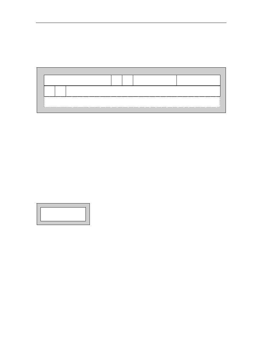
Appendix A. Instruction Set Details A-97
Mask
MASK
Format:
RRconst format
OP-code 0001 01
Rd-code
Rs-code
15
8 7
4 3
0
cosnt2
s = 0: Rs-code encodes G0..G15 for Rs, s = 1: Rs-code encodes L0..L15 for Rs
d = 0: Rd-code encodes G0..G15 for Rd, d = 1: Rd-code encodes L0..L15 for Rd
S : Sign bit of dis, e = 0: const = 18S // const1 (range -16,384..16,383)
e = 1: const = 2S // const1 // const2 (range -1,073,741,824...1,073,741,823)
e
const1
S
d
s
Notation:
MASK Rd, Rs, const
Description:
The result of a bitwise logical AND of the source operand and the immediate operand is
placed in the destination register and the Z flag is set or cleared accordingly.
All operands and the result are interpreted as bit-string of 32 bits each.
Operation:
Rs := Rd and const;
Z := Rd = 0;
Exceptions:
None.

A-98 Appendix A. Instruction Set Details
Move Word
MOV
Format:
RR format
Rd-code
Rs-code
OP-code
0010 01
d
s
15
10
9
8
7
4 3
0
s = 0: Rs-code encoded G0..G15 for Rs
s = 1: Rs-code encoded L0..L15 for Rs
d = 0: Rd-code encoded G0..G15 for Rd
d = 1: Rd-code encoded L0..L15 for Rd
Notation:
MOV Rd, Rs
Description:
The source operand is copied to the destination register and condition flags are set or
cleared accordingly.
Operation:
Rd := Rs;
Z := Rd = 0;
N := Rd(31);
V := Undefined
Exceptions:
None.

Appendix A. Instruction Set Details A-99
Move Double Word
MOVD
Format:
RR format
Rd-code
Rs-code
OP-code
0000 01
d
s
15
10
9
8
7
4 3
0
s = 0: Rs-code encoded G0..G15 for Rs
s = 1: Rs-code encoded L0..L15 for Rs
d = 0: Rd-code encoded G0..G15 for Rd
d = 1: Rd-code encoded L0..L15 for Rd
Notation:
MOVD Rd, Rs
MOVD Rd, 0 (When SR is denoted as a source operand)
Description:
The double-word source operand is copied to the double-word destination register pair and
condition flags are set or cleared accordingly. The high-order word in Rs is copied first.
When the SR is denoted as a source operand, the source operand is supplied as zero
regardless of the content of SR//G2. When the PC is denoted as destination, the Return
instruction RET is executed instead of the Move Double-Word instruction.
Operation:
If Rd does not denote PC and
Rs does not denote SR then
Rd := Rs;
Rdf := Rsf;
Z := Rd//Rsf = 0;
N := Rd(31);
V := Undefined
If Rd does not denote PC and
Rs denotes SR then
Rd := 0;
Rdf := 0;
Z := 1;
N := 0;
V := Undefined
Exceptions:
None.

A-100 Appendix A. Instruction Set Details
Move Word Immediate
MOVI
Format:
Rimm format
15
8 7
4 3
0
imm2
d = 0: Rd-code encodes G0..G15 for Rd, d = 1: Rd-code encodes L0..L15 for Rd
n: Bit 8 // bits 3..0 encode n = 0..31, see Table 2.3 Encoding of Immediate Values for encoding of imm
imm1
OP-code 0110 01
Rd-code
n
d
n
Notation:
MOVI Rd, imm
Description:
The immediate operand is copied to the destination register and condition flags are set or
cleared accordingly.
Operation:
Rs := imm;
Z := Rd = 0;
N := Rd(31);
V := 0;
Exceptions:
None.

Appendix A. Instruction Set Details A-101
Multiply Word
MUL
Format:
RR format
OP-code
1011 11
Rs-code
s
d
Rd-code
15
10
9
8
7
4 3
0
s = 0: Rs-code encoded G0..G15 for Rs
s = 1: Rs-code encoded L0..L15 for Rs
d = 0: Rd-code encoded G0..G15 for Rd
d = 1: Rd-code encoded L0..L15 for Rd
Notation:
MUL Rd, Rs
Description:
The source operand and the destination operand are multiplied, the low-order word of the
product is placed in the destination register (the high-order product word is not evaluated)
and the condition flags are set or cleared according to the single-word product.
Both operands are either signed or unsigned integers, the product is a single-word integer.
The result is undefined if the PC or the SR is denoted.
Operation:
Rs := low order word of product Rd * Rs;
Z := sinlgeword product = 0;
N := Rd(31);
- sing of singleword product;
- valid for singed operands;
V := undefined;
C := undefined;
Exceptions:
None.

A-102 Appendix A. Instruction Set Details
Multiply Signed Double-Word
MULS
Format:
RR format
OP-code
1011 01
Rs-code
s
d
Rd-code
15
10
9
8
7
4 3
0
s = 0: Rs-code encoded G0..G15 for Rs
s = 1: Rs-code encoded L0..L15 for Rs
d = 0: Rd-code encoded G0..G15 for Rd
d = 1: Rd-code encoded L0..L15 for Rd
Notation:
MULS Rd, Rs
Description:
The source operand and the destination operand are multiplied, the double-word product is
placed in the destination register pair (the destination register expanded by the register
following it) and the condition flags are set or cleared according to the double-word
product.
Both operands are signed integers and the product is a signed double-word integer.
The result is undefined if the PC or the SR is denoted.
Operation:
Rs//Rdf := signed doubleword product Rd * Rs;
Z := Rd//Rdf = 0;
- doubleword product is zero
N := Rd(31);
- doubleword product is negative
V := undefined;
C := undefined;
Exceptions:
None.

Appendix A. Instruction Set Details A-103
Multiply Unsigned Double-Word
MULU
Format:
RR format
OP-code
1011 00
Rs-code
s
d
Rd-code
15
10
9
8
7
4 3
0
s = 0: Rs-code encoded G0..G15 for Rs
s = 1: Rs-code encoded L0..L15 for Rs
d = 0: Rd-code encoded G0..G15 for Rd
d = 1: Rd-code encoded L0..L15 for Rd
Notation:
MULU Rd, Rs
Description:
The source operand and the destination operand are multiplied, the double-word product is
placed in the destination register pair (the destination register expanded by the register
following it) and the condition flags are set or cleared according to the double-word
product.
Both operands are unsigned integers and the product is a unsigned double-word integer.
The result is undefined if the PC or the SR is denoted.
Operation:
Rs//Rdf := unsigned doubleword product Rd * Rs;
Z := Rd//Rdf = 0;
- doubleword product is zero
N := Rd(31);
V := undefined;
C := undefined;
Exceptions:
None.

A-104 Appendix A. Instruction Set Details
Negate (unsigned or unsigned)
NEG
Format:
RR format
OP-code
0101 10
Rs-code
s
d
Rd-code
15
10
9
8
7
4 3
0
s = 0: Rs-code encoded G0..G15 for Rs
s = 1: Rs-code encoded L0..L15 for Rs
d = 0: Rd-code encoded G0..G15 for Rd
d = 1: Rd-code encoded L0..L15 for Rd
Notation:
NEG Rd, Rs
NEG Rd, C (when SR is denoted as a Rs)
Description:
The source operand (Rs) is subtracted from zero, the result is placed in the destination
register (Rd) and the condition flag are set or cleared accordingly.
Both operands and the result are interpreted as either all signed or all unsigned integers.
When the SR is denoted as a source operand, carry flag C is negated instead of the SR.
Operation:
When Rs is SR
Rd := - C;
Z := Rd = 0; N := Rd(31);
V := overflow; C := carry;
if C is set then Rd := -1;
else Rd := 0;
When Rs is not SR
Rd := - Rs;
Z := Rd = 0;
N := Rd(31);
V := overflow;
C := carry;
Exceptions:
None.

Appendix A. Instruction Set Details A-105
Negate (signed)
NEGS
Format:
RR format
OP-code
0101 11
Rs-code
s
d
Rd-code
15
10
9
8
7
4 3
0
s = 0: Rs-code encoded G0..G15 for Rs
s = 1: Rs-code encoded L0..L15 for Rs
d = 0: Rd-code encoded G0..G15 for Rd
d = 1: Rd-code encoded L0..L15 for Rd
Notation:
NEGS Rd, Rs
NEGS Rd, C (when SR is denoted as a Rs)
Description:
The source operand (Rs) is subtracted from zero, the result is placed in the destination
register (Rd) and the condition flag are set or cleared accordingly.
Both operands and the result are interpreted as all signed.
When the SR is denoted as a source operand, carry flag C is negated instead of the SR.
Operation:
When Rs is SR
Rd := - C;
Z := Rd = 0;
N := Rd(31);
V := overflow; C := carry;
if C is set then Rd := -1;
else Rd := 0;
When Rs is not SR
Rd := - Rs;
Z := Rd = 0;
N := Rd(31);
V := overflow;
if overflow then
trap => Range Error
Exceptions:
Overflow: Range Error.

A-106 Appendix A. Instruction Set Details
No Operation
NOP
Format:
RR format
OP-code
0000 00
Rs-code (L0)
0000
s
1
d
1
Rd-code (L0)
0000
15
10
9
8
7
4 3
0
Notation:
NOP
Description:
The instruction CHK L0, L0 cannot cause any trap. Since CHK leaves all registers and
condition flags unchanged, it can be used as a No Operation instruction.
Operation:
None.
Exceptions:
None.

Appendix A. Instruction Set Details A-107
Invert
NOT
Format:
RR format
OP-code
0100 01
Rs-code
s
d
Rd-code
15
10
9
8
7
4 3
0
s = 0: Rs-code encoded G0..G15 for Rs
s = 1: Rs-code encoded L0..L15 for Rs
d = 0: Rd-code encoded G0..G15 for Rd
d = 1: Rd-code encoded L0..L15 for Rd
Notation:
NOT Rd, Rs
Description:
The source operand (Rs) is placed bitwise inverted in the designation register and the Z
flag is set or cleared accordingly.
The source operand and the result are interpreted as bit-strings of 32 bits each.
Operation:
Rd := not Rs;
Z := Rd = 0;
Exceptions:
None.

A-108 Appendix A. Instruction Set Details
OR
OR
Format:
RR format
OP-code
0011 10
Rs-code
s
d
Rd-code
15
10
9
8
7
4 3
0
s = 0: Rs-code encoded G0..G15 for Rs
s = 1: Rs-code encoded L0..L15 for Rs
d = 0: Rd-code encoded G0..G15 for Rd
d = 1: Rd-code encoded L0..L15 for Rd
Notation:
OR Rd, Rs
Description:
The result of a bitwise logical OR of the source operand and the destination operand is
placed in the destination register and the Z flag is set or cleared accordingly.
All operands and the result are interpreted as bit-strings of 32 bits each.
Operation:
Rs := Rd or Rs;
Z := Rd = 0;
Exceptions:
None.

Appendix A. Instruction Set Details A-109
OR Immediate
ORI
Format:
Rimm format
15
8 7
4 3
0
imm2
d = 0: Rd-code encodes G0..G15 for Rd, d = 1: Rd-code encodes L0..L15 for Rd
n: Bit 8 // bits 3..0 encode n = 0..31, see Table 2.3 Encoding of Immediate Values for encoding of imm
imm1
OP-code 0111 10
Rd-code
n
d
n
Notation:
ORI Rd, imm
Description:
The result of a bitwise logical OR of the immediate operand and the destination operand is
placed in the destination register and the Z flag is set or cleared accordingly.
All operands and the result are interpreted as bit-strings of 32 bits each.
Operation:
Rs := Rd or imm;
Z := Rd = 0;
Exceptions:
None.

A-110 Appendix A. Instruction Set Details
Return
RET
Format:
RR format
OP-code
0000 01
Rs-code
s
d
Rd-code
15
10
9
8
7
4 3
0
s = 0: Rs-code encoded G0..G15 for Rs
s = 1: Rs-code encoded L0..L15 for Rs
d = 0: Rd-code encoded G0..G15 for Rd
d = 1: Rd-code encoded L0..L15 for Rd
Notation:
RET PC, Rs
Description:
The Return instruction returns control from a subprogram entered through a Call, Trap or
Software instruction or an exception to the instruction located at the return address and
restores the status from the saved return status.
The source operand pair Rs//Rsf is placed in the register pair PC//SR. The program counter
PC is restored first from Rs. Then all bits of the status register SR are replaced by Rsf;
except the supervisor flag S, which is restored from bit zero of Rs and except the
instruction length code ILC, which is cleared to zero.
The Return instruction shares its basic OP-code with the Move Double-Word instruction. It
is differentiated from it by denoting the PC as destination register Rd.
Operation:
old S := S; old L := L;
PC := Rs(31..1)//0;
SR := Rs(31..32)//00//Rs(0)//Rsf(17..0); - ILC := 0; S := Rs(0);
If ( old S = 0 and S = 1) or ( S=0 and old L= 0 and L = 1 ) then trap => Privilege Error;
difference(6..0) := FP - SP(8..2); - difference is signed, difference(6) = sign bit
If difference > 0 then continue at next instructio;
else
repeat
SP := SP -4; register SP(7..2)^ := memory SP^;
difference := difference + 1;
until difference = 0;
Exceptions:
Privilege Error.

Appendix A. Instruction Set Details A-111
Rotate Left
ROL
Format:
LL format
OP-code
1000 1111
Ls-code
Ld-code
15
7
4 3
0
Ls-code encodes L0..L15 for Ls
Ld-code encodes L0..L15 for Ld
Notation:
ROL Ld, Ls
Description:
The destination operand is shifted left by a number of bit positions and the bits shifted out
are inserted in the vacated bit positions; thus, the destination operand is rotated. The
condition flags are set or cleared accordingly. Bits 4..0 of the source operand specify a
rotation by 0..31 bit positions; bits 31..5 of the source operand are ignored.
Operation:
Ld := Ld rotated left by Ls(4..0);
Z := Ld = 0;
N := Ld(31);
V := undefined;
C := undefined;
Exceptions:
None.

A-112 Appendix A. Instruction Set Details
Shift Right (Signed Single Word)
SAR
Format:
LL format
OP-code
1000 0111
Ls-code
15
7
4 3
0
Ld-code
Ls-code encodes L0..L15 for Ls
Ld-code encodes L0..L15 for Ld
Notation:
SAR Ld, Ls
Description:
The destination operand is shifted right by a number of bit positions specified by bits 4..0
of the source operand as a shift by 0..31. The higher-order bits of the source operand are
ignored. The destination operand is interpreted as a signed integer.
The Shift Right instruction inserts sign bits in the vacated bit positions at the left.
Operation:
Ld := Ld >> by Ls(4..0);
Z := Ld =0;
N := Ld(31);
C := last bit shifted out is "one"
Exceptions:
None.

Appendix A. Instruction Set Details A-113
Shift Right (Signed Double Word)
SARD
Format:
LL format
OP-code
1000 0110
Ls-code
15
7
4 3
0
Ld-code
Ls-code encodes L0..L15 for Ls
Ld-code encodes L0..L15 for Ld
Notation:
SARD Ld, Ls
Description:
The destination operand is shifted right by a number of bit positions specified by bits 4..0
of the source operand as a shift by 0..31. The higher-order bits of the source operand are
ignored. The destination operand is interpreted as a signed double-word integer.
The Shift Right instruction inserts sign bits in the vacated bit positions at the left.
The double-word Shift Right instruction executes in two cycles. The high-order operand in
Ld is shifted first. The result is undefined if Ls denotes the same register as Ld or Ldf.
Operation:
Ld//Ldf := Ld//Ldf >> by Ls(4..0);
Z := Ld//Ldf =0;
N := Ld(31);
C := last bit shifted out is "one"
Exceptions:
None.

A-114 Appendix A. Instruction Set Details
Shift Right Immediate (Signed Double Word)
SARDI
Format:
Ln format
OP-code
1000 010
n
n
15
7
4 3
0
Ld-code encodes L0..L15 for Ld
n: Bit 8//bit 3..0 encode n = 0..31
Ld-code
8
9
Notation:
SARDI Ld, n
Description:
The destination operand is shifted right by a number of bit positions specified by n = 0..31
as a shift by 0..31. The destination operand is interpreted as a signed double-word integer.
The Shift Right instruction inserts sign bits in the vacated bit positions at the left.
The double-word Shift Right instruction executes in two cycles. The high-order operand in
Ld is shifted first. The result is undefined if Ls denotes the same register as Ld or Ldf.
Operation:
Ld//Ldf := Ld//Ldf >> by n;
Z := Ld//Ldf = 0;
N := Ld(31);
C := last bit shifted out is "one"
Exceptions:
None.

Appendix A. Instruction Set Details A-115
Shift Right Immediate (Signed Single Word)
SARI
Format:
Rn format
OP-code
1010 01
n
n
15
7
4 3
0
d = 0: Rd-code encodes G0..G15 for Rd
d = 1: Rd-code encodes L0..L15 for Rd
n: Bit 8//bit 3..0 encode n = 0..31
Rd-code
8
9
d
Notation:
SARI Ld, n
Description:
The destination operand is shifted right by a number of bit positions specified by n = 0..31
as a shift by 0..31. The destination operand is interpreted as a signed integer.
The Shift Right instruction inserts sign bits in the vacated bit positions at the left.
Operation:
Ld := Ld >> by n;
Z := Ld/ = 0;
N := Ld(31);
C := last bit shifted out is "one"
Exceptions:
None.

A-116 Appendix A. Instruction Set Details
Shift Left (Single Word)
SHL
Format:
LL format
OP-code
1000 1011
Ls-code
15
7
4 3
0
Ld-code encodes L0..L15 for Ld
Ls-code encodes L0..L15 for Ls
Ld-code
8
Notation:
SHL Ld, Ls
Description:
The destination operand is shifted left by a number of bit positions specified by bits 4..0 of
the source operand as a shift by 0..31. The higher-order bits of the source operand are
ignored. The destination operand is interpreted as a signed or unsigned integer.
The Shift Left instruction inserts zeros in the vacated bit positions at the right.
Operation:
Ld := Ld << by Ls(4..0);
Z := Ld = 0;
N := Ld(31);
C := undefined;
V := undefined;
Exceptions:
None.

Appendix A. Instruction Set Details A-117
Shift Left (Double Word)
SHLD
Format:
LL format
OP-code
1000 1010
Ls-code
15
7
4 3
0
Ld-code encodes L0..L15 for Ld
Ls-code encodes L0..L15 for Ls
Ld-code
8
Notation:
SHLD Ld, Ls
Description:
The destination operand is shifted left by a number of bit positions specified by bits 4..0 of
the source operand as a shift by 0..31. The higher-order bits of the source operand are
ignored. The destination operand is interpreted as a signed or unsigned double-word
integer.
The Shift Left instruction inserts zeros in the vacated bit positions at the right.
The double-word Shift Left instruction executes in two cycles. The high-order operand in
Ld is shifted first. The result is undefined if Ls denotes the same register as Ld or Ldf.
Operation:
Ld//Ldf := Ld//Ldf << by Ls(4..0);
Z := Ld//Ldf = 0;
N := Ld(31);
C := undefined;
V := undefined;
Exceptions:
None.

A-118 Appendix A. Instruction Set Details
Shift Left Immediate (Double Word)
SHLDI
Format:
Ln format
OP-code
1000 100
n
15
7
4 3
0
Ld-code encodes L0..L15 for Ld
n: Bit 8//bit 3..0 encode n = 0..31
Ld-code
8
n
9
Notation:
SHLDI Ld, n
Description:
The destination operand is shifted left by a number of bit positions specified by n = 0..31
as a shift by 0..31. The destination operand is interpreted as a signed or unsigned double-
word integer.
The Shift Left instruction inserts zeros in the vacated bit positions at the right.
The double-word Shift Left instruction executes in two cycles. The high-order operand in
Ld is shifted first. The result is undefined if Ls denotes the same register as Ld or Ldf.
Operation:
Ld//Ldf := Ld//Ldf << by n;
Z := Ld//Ldf = 0;
N := Ld(31);
C := undefined;
V := undefined;
Exceptions:
None.

Appendix A. Instruction Set Details A-119
Shift Left Immediate (Single Word)
SHLI
Format:
Rn format
OP-code
1010 10
n
n
15
7
4 3
0
d = 0: Rd-code encodes G0..G15 for Rd
d = 1: Rd-code encodes L0..L15 for Rd
n: Bit 8//bit 3..0 encode n = 0..31
Rd-code
8
9
d
Notation:
SHLI Ld, n
Description:
The destination operand is shifted left by a number of bit positions specified by n = 0..31
as a shift by 0..31. The destination operand is interpreted as a signed or unsigned integer.
The Shift left instruction inserts zeros in the vacated bit positions at the right.
Operation:
Ld := Ld << by n;
Z := Ld = 0;
N := Ld(31);
C := undefined;
V := undefined;
Exceptions:
None.

A-120 Appendix A. Instruction Set Details
Shift Right (Unsigned Single Word)
SHR
Format:
LL format
OP-code
1000 0011
Ls-code
15
7
4 3
0
Ld-code encodes L0..L15 for Ld
Ls-code encodes L0..L15 for Ls
Ld-code
8
Notation:
SHR Ld, Ls
Description:
The destination operand is shifted right by a number of bit positions specified by bits 4..0
of the source operand as a shift by 0..31. The higher-order bits of the source operand are
ignored. The destination operand is interpreted as a unsigned integer.
The Shift Right instruction inserts zeros in the vacated bit positions at the left.
Operation:
Ld := Ld >> by Ls(4..0);
Z := Ld =0;
N := Ld(31);
C := last bit shifted out is "one"
Exceptions:
None.

Appendix A. Instruction Set Details A-121
Shift Right (Unsigned Double Word)
SHRD
Format:
LL format
OP-code
1000 0010
Ls-code
15
7
4 3
0
Ld-code encodes L0..L15 for Ld
Ls-code encodes L0..L15 for Ls
Ld-code
8
Notation:
SHRD Ld, Ls
Description:
The destination operand is shifted right by a number of bit positions specified by bits 4..0
of the source operand as a shift by 0..31. The higher-order bits of the source operand are
ignored. The destination operand is interpreted as a unsigned double-word integer.
The Shift Right instruction inserts zeros in the vacated bit positions at the left.
The double-word Shift Right instruction executes in two cycles. The high-order operand in
Ld is shifted first. The result is undefined if Ls denotes the same register as Ld or Ldf.
Operation:
Ld//Ldf := Ld//Ldf >> by Ls(4..0);
Z := Ld//Ldf =0;
N := Ld(31);
C := last bit shifted out is "one"
Exceptions:
None.

A-122 Appendix A. Instruction Set Details
Shift Right Immediate (Unsigned Double Word)
SHRDI
Format:
Ln format
OP-code
1000 000
n
15
7
4 3
0
Ld-code encodes L0..L15 for Ld
n: Bit 8//bit 3..0 encode n = 0..31
Ld-code
8
n
9
Notation:
SHRDI Ld, n
Description:
The destination operand is shifted right by a number of bit positions specified by n = 0..31
as a shift by 0..31. The destination operand is interpreted as a unsigned double-word
integer.
The Shift Right instruction inserts zeros in the vacated bit positions at the left.
The double-word Shift Right instruction executes in two cycles. The high-order operand in
Ld is shifted first. The result is undefined if Ls denotes the same register as Ld or Ldf.
Operation:
Ld//Ldf := Ld//Ldf >> by n;
Z := Ld//Ldf = 0;
N := Ld(31);
C := last bit shifted out is "one"
Exceptions:
None.

Appendix A. Instruction Set Details A-123
Shift Right Immediate (Unsigned Single Word)
SHRI
Format:
Rn format
OP-code
1010 00
n
n
15
7
4 3
0
d = 0: Rd-code encodes G0..G15 for Rd
d = 1: Rd-code encodes L0..L15 for Rd
n: Bit 8//bit 3..0 encode n = 0..31
Rd-code
8
9
d
Notation:
SHRI Ld, n
Description:
The destination operand is shifted right by a number of bit positions specified by n = 0..31
as a shift by 0..31. The destination operand is interpreted as a unsigned integer.
The Shift Right instruction inserts zeros in the vacated bit positions at the left.
Operation:
Ld := Ld >> by n;
Z := Ld/ = 0;
N := Ld(31);
C := last bit shifted out is "one"
Exceptions:
None.

A-124 Appendix A. Instruction Set Details
Set Stack Address
SETADR
Format:
Rn format
OP-code
1011 10
n
0000
d
15
7
4 3
0
d = 0: Rd-code encodes G0..G15 for Rd
d = 1: Rd-code encodes L0..L15 for Rd
n:
Bit 8 // bits 3..0 encode n = 0..31
n
0
Rd-code
Notation:
SETADR Rd
Description:
The Set Stack Address instruction calculates the stack address of the beginning of the
current stack frame. L0..L15 of this frame can then be addressed relative to this stack
address in the stack address mode with displacement values of 0..60 respectively.
The frame pointer FP is placed, expanded to the stack address, in the destination register.
The FP itself and all condition flags remain unchanged. The expanded FP address is the
address at which the content of L0 would be stored if pushed onto the memory part of the
stack.
The Set Stack Address instruction shares the basic OP-code SETxx, it is differentiated by n
= 0 and not denoting the SR or the PC.
Operation:
Rd := SP(31..9) // SR(31..25) // 00 + carry into bit 9
- SR(31..25) is FP
- carry into bit 9 := ( SP(8)=1 and SR(31)=0 )
Exceptions:
None.

Appendix A. Instruction Set Details A-125
Set Conditional Instruction
SETxx
Format:
Rn format
OP-code
1011 10
n
d
15
7
4 3
0
d = 0: Rd-code encodes G0..G15 for Rd
d = 1: Rd-code encodes L0..L15 for Rd
n:
Bit 8 // bits 3..0 encode n = 0..31
n
Rd-code
Notation:
SETxx Rd
Description:
The destination register is set or cleared according to the states of the condition flags
specified by n. The condition flags themselves remain unchanged.
The Set Conditional instruction share the basic OP-code SETxx, they are differentiated by
n = 1..31 and not denoting the SR or the PC.
l n = 0 while not denoting the SR or the PC differentiates the Set Stack Address
instruction.
l n = 1..31 while not denoting the SR or the PC differentiates the Set Conditional
instruction.
l Denoting the SR differentiates the Fetch instruction.
l Denoting the PC is reserved for future use.
Operation:
n Notation or Alternative Operation
1 Reserved
2 SET1 Rd Rd := 1;
3 SET0 Rd Rd := 0;
4 SETLE Rd if N = 1 or Z = 1 then Rd := 1 else Rd := 0;
5 SETGT Rd if N = 0 and Z = 0 then Rd := 1 else Rd := 0;
6 SETLT Rd SETN Rd if N = 1 then Rd := 1 else Rd := 0;
7 SETGE Rd SETNN Rd if N = 0 then Rd := 1 else Rd := 0;
8 SETSE Rd if C = 1 or Z = 1 then Rd := 1 else Rd := 0;
9 SETHT Rd if C = 0 and Z = 0 then Rd := 1 else Rd := 0;
10 SETST Rd SETC Rd if C = 1 then Rd := 1 else Rd := 0;

A-126 Appendix A. Instruction Set Details
Set Conditional Instruction (continued)
SETxx
n Notation or Alternative Operation
11 SETHE Rd SETNC Rd if C = 0 then Rd := 1 else Rd := 0;
12 SETE SETZ if Z = 1 then Rd := 1 else Rd := 0;
13 SETNE SETNZ if Z = 0 then Rd := 1 else Rd := 0;
14 SETV Rd if V = 1 then Rd := 1 else Rd := 0;
15 SETNV Rd if V = 0 then Rd := 1 else Rd := 0;
16 Reserved
17 Reserved
18 SET1M Rd Rd := -1;
19 Reserved
20 SETLEM Rd if N = 1 or Z = 1 then Rd := -1 else Rd := 0;
21 SETGTM Rd if N = 0 and Z = 0 then Rd := -1 else Rd := 0;
22 SETLTM Rd SETNM Rd if N = 1 then Rd := -1 else Rd := 0;
23 SETGEM Rd SETNNM Rd if N = 0 then Rd := -1 else Rd := 0;
24 SETSEM Rd if C = 1 or Z = 1 then Rd := -1 else Rd := 0;
25 SETHTM Rd if C = 0 and Z = 0 then Rd := -1 else Rd := 0;
26 SETSTM Rd SETCM Rd if C = 1 then Rd := -1 else Rd := 0;
27 SETHEM Rd SETNCM Rd if C = 0 then Rd := -1 else Rd := 0;
28 SETEM SETZM if Z = 1 then Rd := -1 else Rd := 0;
29 SETNEM SETNZM if Z = 0 then Rd := -1 else Rd := 0;
30 SETVM Rd if V = 1 then Rd := -1 else Rd := 0;
31 SETNVM Rd if V = 0 then Rd := -1 else Rd := 0;
Exceptions:
None.
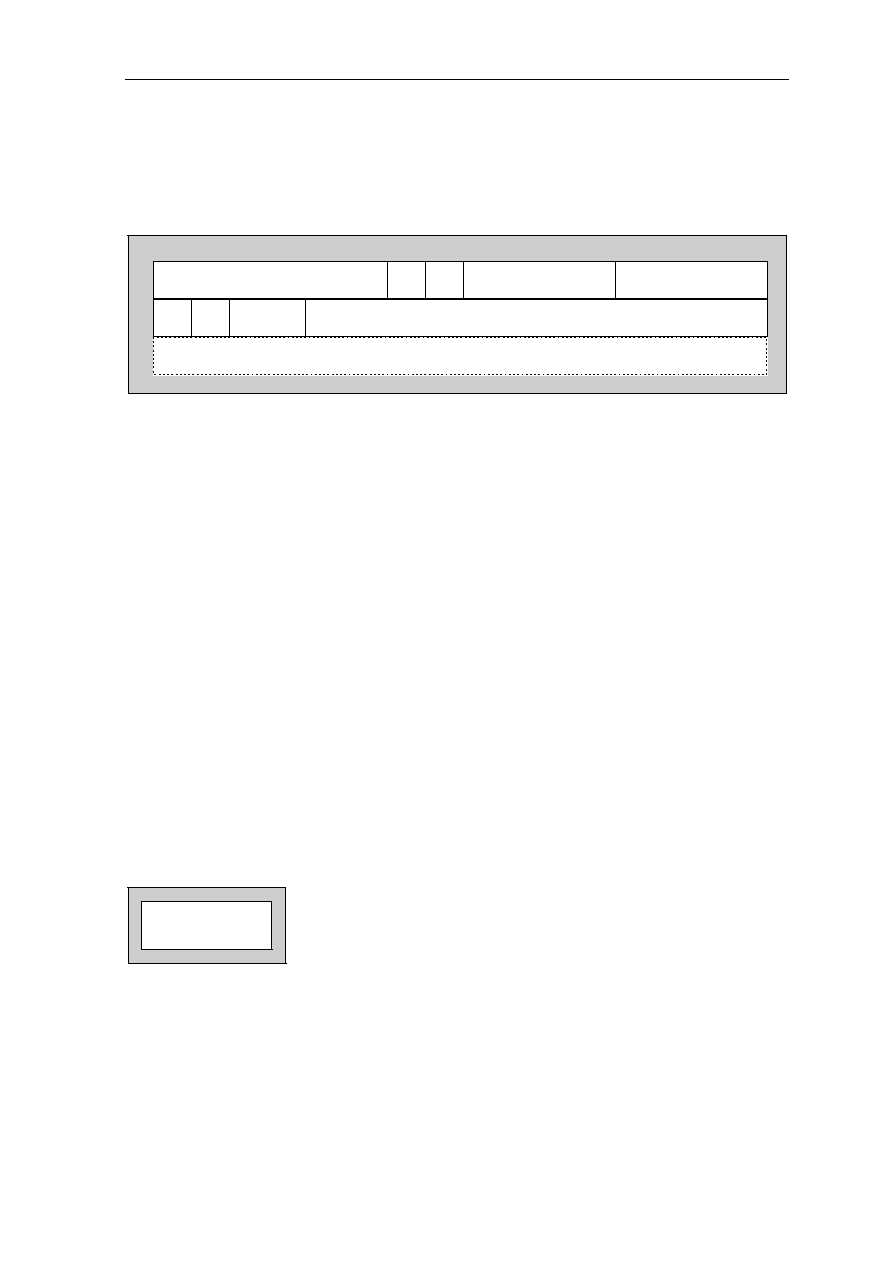
Appendix A. Instruction Set Details A-127
Store (absolute address mode)
STxx.A
Format:
RRdis format
OP-code 1001 10
Rd-code
Rs-code
15
8 7
4 3
0
dis2
s = 0: Rs-code encodes G0..G15 for Rs, s = 1: Rs-code encodes L0..L15 for Rs
d = 0: Rd-code encodes G0..G15 for Rd, d = 1: Rd-code encodes L0..L15 for Rd
S : Sign bit of dis, e = 0: dis = 20S // dis1(range -4,096..4,095)
e = 1: dis = 4S // dis1 // dis2 (range -268,435,456...268,435,455)
DD: D-code, D13..D12 encode data types at memory instructions
e
dis1
S
d
s
DD
Notation:
STxx.A 0, Rs, dis
Description:
The Store instruction of absolute address mode transfers data from a register Rs or a
register pair Rs//Rsf into the addressed memory location, displacement dis is used as an
address.
The displacement dis is used as an address into memory address space. Rd must denote the
SR to differentiate this mode from the displacement address mode; the content of the SR is
not used.
Data type xx is with
BU: Byte unsigned HU: Halfword unsigned W: Word
BS: Byte singed HS: Halfword signed D: Double-word
Operation:
dis^ := Rs;
[(dis+4)^ := Rsf;]
Exceptions:
None.

A-128 Appendix A. Instruction Set Details
Store Double Word (post-increment address mode)
STD.P
Format:
LR format
OP-code
1101 111
Ld-code
Rs-code
15
8 7
4 3
0
s = 0: Rs-code encodes G0..G15 for Rs
s = 1: Rs-code encodes L0..L15 for Rs
Ld-code encodes L0..L15 for Ld
s
Notation:
STD.P Ld, Rs
Description:
The Store instruction of post-increment address mode transfers data from a register pair
Rs//Rsf into the addressed memory location, Ld is used as an address.
The content of the destination register Ld is used as an address into memory address space,
then Ld is incremented according to the specified data size of double-word memory
instruction by 8, regardless of any exception occurring. Ld is incremented by 8 at the first
memory cycle.
Operation:
Ld^ := Rs; Ld := Ld +size;
(old Ld + 4)^ := Rsf;
Exceptions:
None.

Appendix A. Instruction Set Details A-129
Store Double Word (register address mode)
STD.R
Format:
LR format
OP-code
1101 101
Ld-code
Rs-code
15
8 7
4 3
0
s = 0: Rs-code encodes G0..G15 for Rs
s = 1: Rs-code encodes L0..L15 for Rs
Ld-code encodes L0..L15 for Ld
s
Notation:
STD.R Ld, Rs
Description:
The Store instruction of register address mode transfers data from a register pair Rs//Rsf
into the addressed memory location, Ld is used as an address.
The content of the destination register Ld is used as an address into memory address space.
Operation:
Ld^ := Rs;
(Ld + 4)^ := Rsf;
Exceptions:
None.

A-130 Appendix A. Instruction Set Details
Store (displacement address mode)
STxx.D
Format:
RRdis format
OP-code 1001 10
Rd-code
Rs-code
15
8 7
4 3
0
dis2
s = 0: Rs-code encodes G0..G15 for Rs, s = 1: Rs-code encodes L0..L15 for Rs
d = 0: Rd-code encodes G0..G15 for Rd, d = 1: Rd-code encodes L0..L15 for Rd
S : Sign bit of dis, e = 0: dis = 20S // dis1(range -4,096..4,095)
e = 1: dis = 4S // dis1 // dis2 (range -268,435,456...268,435,455)
DD: D-code, D13..D12 encode data types at memory instructions
e
dis1
S
d
s
DD
Notation:
STxx.D Rd, Rs, dis
Description:
The Store instruction of displacement address mode transfers data from a register Rs or a
register pair Rs//Rsf. into the addressed memory location, Rd plus a signed dis is used as
an address.
The sum of the contents of the destination register Rd plus a signed displacement dis is
used as an address into memory address space.
Rd may denote any register except the SR; Rd not denoting the SR differentiates this mode
from the absolute address mode.
Data type xx is with
BU: Byte unsigned HU: Halfword unsigned W: Word
BS: Byte singed HS: Halfword signed D: Double-word
Operation:
(Rd + dis)^ := Rs;
[(Rd + dis +4)^ := Rsf;]
Exceptions:
None.
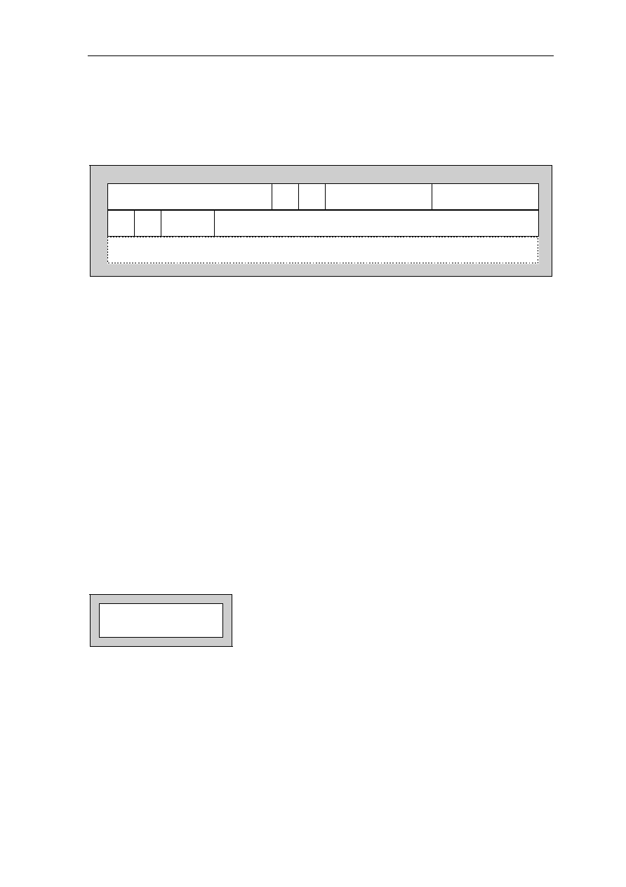
Appendix A. Instruction Set Details A-131
Store (I/O absolute address mode)
STxx.IOA
Format:
RRdis format
OP-code 1001 10
Rd-code
Rs-code
15
8 7
4 3
0
dis2
s = 0: Rs-code encodes G0..G15 for Rs, s = 1: Rs-code encodes L0..L15 for Rs
d = 0: Rd-code encodes G0..G15 for Rd, d = 1: Rd-code encodes L0..L15 for Rd
S : Sign bit of dis, e = 0: dis = 20S // dis1(range -4,096..4,095)
e = 1: dis = 4S // dis1 // dis2 (range -268,435,456...268,435,455)
DD: D-code, D13..D12 encode data types at memory instructions
e
dis1
S
d
s
DD
Notation:
STxx.IOA 0, Rs, dis
Description:
The Store instruction of I/O absolute address mode transfers data from a register Rs or a
register pair Rs//Rsf into the addressed memory location, dis is used as an address.
The displacement dis is used as an address into I/O address space.
Rd must denote the SR to differentiate this mode from the I/O displacement address mode;
the content of the SR is not used.
Data type xx is with
W: Word D: Double-word
Operation:
dis^ := Rs;
[(dis +4)^ := Rsf;]
Exceptions:
None.

A-132 Appendix A. Instruction Set Details
Store (I/O displacement address mode)
STxx.IOD
Format:
RRdis format
OP-code 1001 10
Rd-code
Rs-code
15
8 7
4 3
0
dis2
s = 0: Rs-code encodes G0..G15 for Rs, s = 1: Rs-code encodes L0..L15 for Rs
d = 0: Rd-code encodes G0..G15 for Rd, d = 1: Rd-code encodes L0..L15 for Rd
S : Sign bit of dis, e = 0: dis = 20S // dis1(range -4,096..4,095)
e = 1: dis = 4S // dis1 // dis2 (range -268,435,456...268,435,455)
DD: D-code, D13..D12 encode data types at memory instructions
e
dis1
S
d
s
DD
Notation:
STxx.IOD Rd, Rs, dis
Description:
The Store instruction of I/O displacement address mode transfers data from a register Rs or
a register pair Rs//Rsf. into the addressed memory location, Rd plus a signed dis is used as
an address.
The sum of the contents of the destination register Rd plus a signed displacement dis is
used as an I/O address into memory address space.
Rd may denote any register except the SR; Rd not denoting the SR differentiates this mode
from the I/O absolute address mode.
Data type xx is with
W: Word D: Double-word
Operation:
(Rd + dis)^ := Rs;
[(Rd + dis +4)^ := Rsf;]
Exceptions:
None.
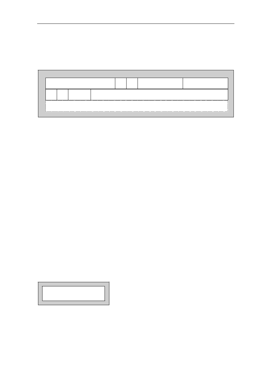
Appendix A. Instruction Set Details A-133
Store (next address mode)
STxx.N
Format:
RRdis format
OP-code 1001 11
Rd-code
Rs-code
15
8 7
4 3
0
dis2
s = 0: Rs-code encodes G0..G15 for Rs, s = 1: Rs-code encodes L0..L15 for Rs
d = 0: Rd-code encodes G0..G15 for Rd, d = 1: Rd-code encodes L0..L15 for Rd
S : Sign bit of dis, e = 0: dis = 20S // dis1(range -4,096..4,095)
e = 1: dis = 4S // dis1 // dis2 (range -268,435,456...268,435,455)
DD: D-code, D13..D12 encode data types at memory instructions
e
dis1
S
d
s
DD
Notation:
STxx.N Rd, Rs, dis
Description:
The Store instruction of next address mode transfers data from a register Rs or a register
pair Rs//Rsf into the addressed memory location, Rd is used as an address.
The content of the destination register Rd is used as an address into memory address space,
then Rd is incremented by the signed displacement dis regardless of any exception
occurring. At a double-word data type, Rd is incremented at the first memory cycle.
Rd must not denote the PC or the SR.
In the case of all data types except byte, bit zero of dis is treated as zero for the calculation
of Rd + dis.
Data type xx is with
BU: Byte unsigned HU: Halfword unsigned W: Word
BS: Byte singed HS: Halfword signed D: Double-word
Operation:
Rd^ := Rs; Rd := Rd + dis;
[(old Rd +4)^ := Rsf;]
Exceptions:
None.

A-134 Appendix A. Instruction Set Details
Store Word (post-increment address mode)
STW.P
Format:
LR format
OP-code
1101 110
Ld-code
Rs-code
15
8 7
4 3
0
s = 0: Rs-code encodes G0..G15 for Rs
s = 1: Rs-code encodes L0..L15 for Rs
Ld-code encodes L0..L15 for Ld
s
Notation:
STW.P Ld, Rs
Description:
The Store instruction of post-increment address mode transfers data from a register Rs into
the addressed memory location, Ld is used as an address.
The content of the destination register Ld is used as an address into memory address space,
then Ld is incremented according to the specified data size of a word by 4, regardless of
any exception occurring.
Operation:
Ld^ := Rs;
Ld := Ld + 4;
Exceptions:
None.

Appendix A. Instruction Set Details A-135
Store Word (register address mode)
STW.R
Format:
LR format
OP-code
1101 100
Ld-code
Rs-code
15
8 7
4 3
0
s = 0: Rs-code encodes G0..G15 for Rs
s = 1: Rs-code encodes L0..L15 for Rs
Ld-code encodes L0..L15 for Ld
s
Notation:
STW.R Ld, Rs
Description:
The Store instruction of register address mode transfers data from into a register Rs into
the addressed memory location, Ld is used as an address.
The content of the destination register Ld is used as an address into memory address space.
Operation:
Ld^ := Rs;
Exceptions:
None.
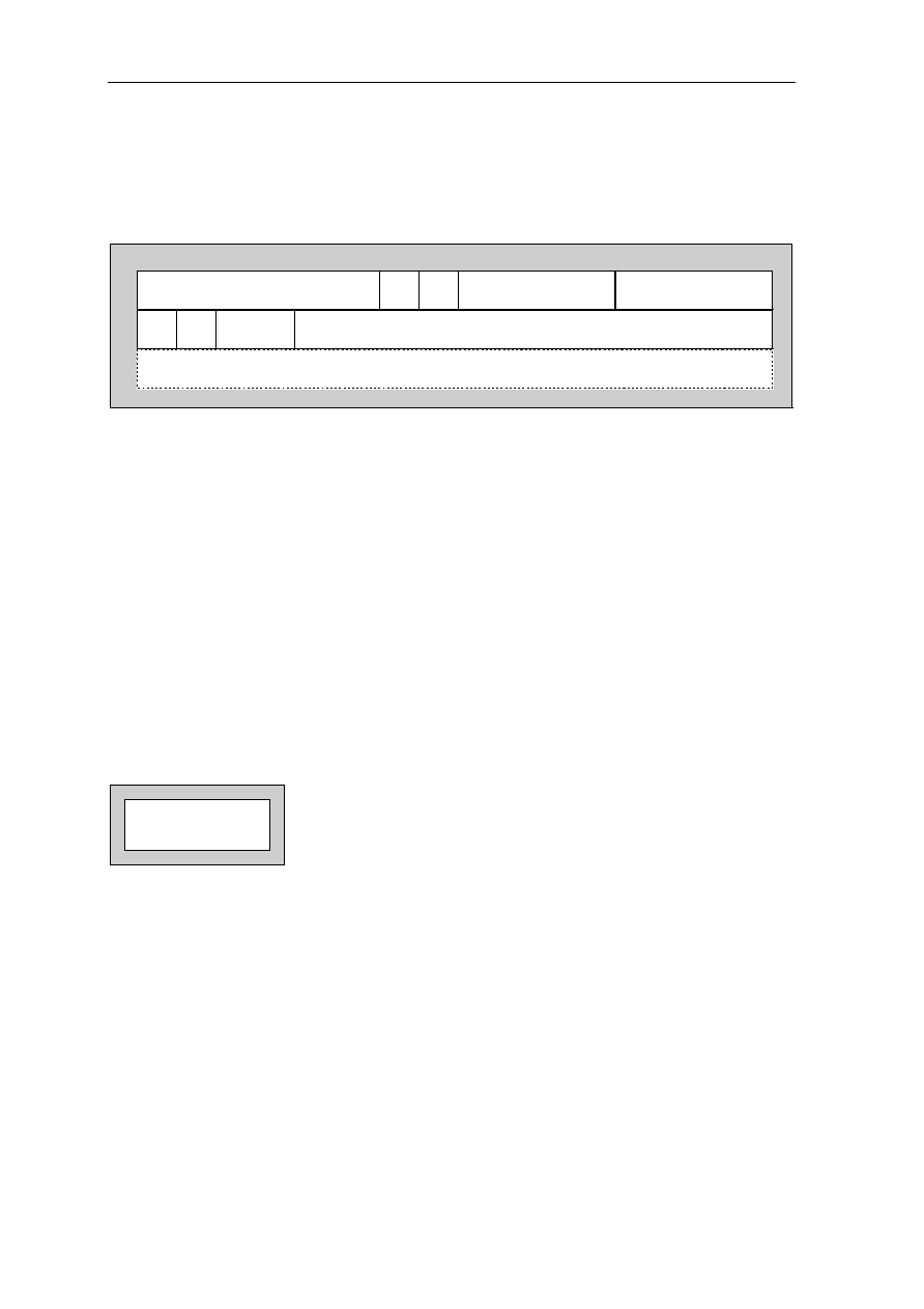
A-136 Appendix A. Instruction Set Details
Store Word (stack address mode)
STW.S
Format:
RRdis format
OP-code 1001 11
Rd-code
Rs-code
15
8 7
4 3
0
dis2
s = 0: Rs-code encodes G0..G15 for Rs, s = 1: Rs-code encodes L0..L15 for Rs
d = 0: Rd-code encodes G0..G15 for Rd, d = 1: Rd-code encodes L0..L15 for Rd
S : Sign bit of dis, e = 0: dis = 20S // dis1(range -4,096..4,095)
e = 1: dis = 4S // dis1 // dis2 (range -268,435,456...268,435,455)
DD: D-code, D13..D12 encode data types at memory instructions
e
dis1
S
d
s
DD
Notation:
STW.S Rd, Rs, dis
Description:
The Store instruction of stack address mode transfers data from into a register Rs into the
addressed memory location, Ld is used as an address.
The content of the destination register Rd is used as stack address, then Rd is incremented
by dis regardless of any exception occurred.
Operation:
Rd^ := Rs;
Rd := Rd + dis;
Exceptions:
None.

Appendix A. Instruction Set Details A-137
Subtract
SUB
Format:
RR format
OP-code
0100 10
Rs-code
d
15
7
4 3
0
s = 0: Rs-code encodes G0..G15 for Rs
s = 1: Rs-code encodes L0..L15 for Rs
d = 0: Rd-code encodes G0..G15 for Rd
d = 1: Rd-code encodes L0..L15 for Rd
s
Rd-code
8
9
Notation:
SUB Rd, Rs
SUB Rd, C (When SR is denoted as a source operand)
Description:
The source operand is subtracted form the destination operand, the result is placed in the
destination register and the condition flags are set or cleared accordingly.
Both operands and the result are interpreted as either all signed or all unsigned integers.
When the SR is denoted as a source operand, C is subtracted instead of the SR.
Operation:
When Rs does not denote SR
Rd := Rd - Rs;
Z := Rd = 0;
N := Rd(31);
V := overflow;
C := borrow;
When Rs denotes SR
Rd := Rd - C;
Z := Rd = 0;
N := Rd(31);
V := overflow;
C := borrow;
Exceptions:
None.

A-138 Appendix A. Instruction Set Details
Subtract with Borrow
SUBC
Format:
RR format
OP-code
0100 00
Rs-code
d
15
7
4 3
0
s = 0: Rs-code encodes G0..G15 for Rs
s = 1: Rs-code encodes L0..L15 for Rs
d = 0: Rd-code encodes G0..G15 for Rd
d = 1: Rd-code encodes L0..L15 for Rd
s
Rd-code
8
9
Notation:
SUBC Rd, Rs
SUBC Rd, C (When SR is denoted as a source operand)
Description:
The source operand + C is subtracted form the destination operand, the result is placed in
the destination register and the condition flags are set or cleared accordingly.
Both operands and the result are interpreted as either all signed or all unsigned integers.
When the SR is denoted as a source operand, C is subtracted instead of the SR.
Operation:
When Rs does not denote SR
Rd := Rd - (Rs + C);
Z := Z and (Rd = 0);
N := Rd(31);
V := overflow;
C := borrow;
When Rs denotes SR
Rd := Rd - C;
Z := Z and (Rd = 0);
N := Rd(31);
V := overflow;
C := borrow;
Exceptions:
None.

Appendix A. Instruction Set Details A-139
Signed Subtract with Trap
SUBS
Format:
RR format
OP-code
0100 11
Rs-code
d
15
7
4 3
0
s = 0: Rs-code encodes G0..G15 for Rs
s = 1: Rs-code encodes L0..L15 for Rs
d = 0: Rd-code encodes G0..G15 for Rd
d = 1: Rd-code encodes L0..L15 for Rd
s
Rd-code
8
9
Notation:
SUBS Rd, Rs
SUBS Rd, C (When SR is denoted as a source operand)
Description:
The source operand is subtracted form the destination operand, the result is placed in the
destination register and the condition flags are set or cleared accordingly.
Both operands and the result are interpreted as all signed integers and a trap to Range Error
occurs at overflow.
When the SR is denoted as a source operand, C is subtracted instead of the SR.
Operation:
When Rs does not denote SR
Rd := Rd - Rs
Z := Rd = 0;
N := Rd(31);
V := overflow;
If overflow then
trap => Range Error
When Rs denotes SR
Rd := Rd - Rs;
Z := Rd = 0;
N := Rd(31);
V := overflow;
If overflow then
trap => Range Error
Exceptions:
Overflow (Trap to Range Error).
A-140 Appendix A. Instruction Set Details
Sum
SUM
Format:
RRconst format
OP-code 0001 10
Rd-code
Rs-code
15
8 7
4 3
0
cosnt2
s = 0: Rs-code encodes G0..G15 for Rs, s = 1: Rs-code encodes L0..L15 for Rs
d = 0: Rd-code encodes G0..G15 for Rd, d = 1: Rd-code encodes L0..L15 for Rd
S : Sign bit of dis, e = 0: const = 18S // const1 (range -16,384..16,383)
e = 1: const = 2S // const1 // const2 (range -1,073,741,824...1,073,741,823)
e
const1
S
d
s
Notation:
SUM Rd, Rs, const
SUM Rd, C, const (When SR is denoted as a source operand)
Description:
The sum of the source operand is placed in the destination register and the condition flags
are set or cleared accordingly.
Both operands and the result are interpreted as either all signed or all unsigned integers.
When the SR is denoted as a source operand, C is added instead of the SR.
Operation:
When Rs does not denote SR
Rd := Rs + const;
Z := Rd = 0;
N := Rd(31);
V := overflow;
C := carry;
When Rs denotes SR
Rd := C + const;
Z := Rd = 0;
N := Rd(31);
V := overflow;
C := carry;
Exceptions:
None.
Appendix A. Instruction Set Details A-141
Signed Sum with Trap
SUMS
Format:
RRconst format
OP-code 0001 11
Rd-code
Rs-code
15
8 7
4 3
0
cosnt2
s = 0: Rs-code encodes G0..G15 for Rs, s = 1: Rs-code encodes L0..L15 for Rs
d = 0: Rd-code encodes G0..G15 for Rd, d = 1: Rd-code encodes L0..L15 for Rd
S : Sign bit of dis, e = 0: const = 18S // const1 (range -16,384..16,383)
e = 1: const = 2S // const1 // const2 (range -1,073,741,824...1,073,741,823)
e
const1
S
d
s
Notation:
SUMS Rd, Rs, const
SUMS Rd, C, const (When SR is denoted as a source operand)
Description:
The sum of the source operand is placed in the destination register and the condition flags
are set or cleared accordingly.
Both operands and the result are interpreted as all signed integers and a trap to Range Error
occurs at overflow.
When the SR is denoted as a source operand, C is added instead of the SR.
Operation:
When Rs does not denote SR
Rd := Rs + const;
Z := Rd = 0;
N := Rd(31);
V := overflow;
If overflow then
trap => Range Error
When Rs denotes SR
Rd := C + const;
Z := Rd = 0;
N := Rd(31);
V := overflow;
If overflow then
trap => Range Error
Exceptions:
Overflow (Trap to Range Error).

A-142 Appendix A. Instruction Set Details
Test Leading Zeros
TESTLZ
Format:
LL format
OP-code
1000 1110
Ls-code
Ld-code
15
7
4 3
0
Ls-code encodes L0..L15 for Ls
Ld-code encodes L0..L15 for Ld
Notation:
TESTLZ Ld, Ls
Description:
The number of leading zeros in the source operand is tested and placed in the destination
register. A source operand equal to zero yields 32 as a result. All condition flags remain
unchanged.
Operation:
Ld := number of leading zeros in Ls;
Exceptions:
None.

Appendix A. Instruction Set Details A-143
Trap
TRAPxx
Format:
PCadr format
OP-code
1111 1101
adr-byte
15
7
0
adr = 24 ones's // adr-byte(7..2) // 00;
8
Notation:
TRAPxx trapno
Description:
The Trap instructions TRAP and any of the conditional Trap instructions when the trap
condition is met, cause a branch to one out of 64 supervisor subprogram entries (see
section 2.4. Entry Tables
).
When the trap condition is not met, instruction execution proceeds sequentially.
When the subprogram branch is taken, the subprogram entry address adr is placed in the
program counter PC and the supervisor-state flag S is set to one. The old PC containing the
return address is saved in the register addressed by FP + FL; the old S flag is also saved in
bit zero of this register. The old status register SR is saved in the register addressed by
FP + FL + 1 (FL = 0 is interpreted as FL = 16); the saved instruction-length code ILC
contains the length (1) of the Trap instruction.
Then the frame pointer FP is incremented by the old frame length FL and FL is set to six,
thus creating a new stack frame. The cache-mode flag M and the trace-mode flag T are
cleared, the interrupt-lock flag L is set to one. All condition flags remain unchanged. Then
instruction execution proceeds at the entry address placed in the PC.
The trap instructions are differentiated by the 12 code values given by the bits 9 and 8 of
the OP-code and bits 1 and 0 of the adr-byte (code = OP(9..8)//adr-byte(1..0)). Since
OP(9..8) = 0 does not denote Trap instructions (the code is occupied by the BR instruction),
trap codes 0..3 are not available.

A-144 Appendix A. Instruction Set Details
Trap (continued)
TRAPxx
Operation:
Code Notation Operation
4 TRAPLE trapno if N = 1 or Z = 1 then execute TRAP else execute next instruction;
5 TRAPGT trapno if N = 0 and Z = 0 then execute TRAP else execute next
instruction;
6 TRAPLT trapno if N = 1 then execute TRAP else execute next instruction;
7 TRAPGE trapno if N = 0 then execute TRAP else execute next instruction;
8 TRAPSE trapno if C = 1 or Z = 1 then execute TRAP else execute next instruction;
9 TRAPHT trapno if C = 0 and Z = 0 then execute TRAP else execute next
instruction;
10 TRAPST trapno if C = 1 then execute TRAP else execute next instruction;
11 TRAPHE trapno if C = 0 then execute TRAP else execute next instruction;
12 TRAPE trapno if Z = 1 then execute TRAP else execute next instruction;
13 TRAPNE trapno if Z = 0 then execute TRAP else execute next instruction;
14 TRAPV trapno if V = 1 then execute TRAP else execute next instruction;
15 TRAP trapno PC := adr;
S := 1;
(FP + FL)^ := old PC(31..1)//old S;
(FP + FL + 1)^ := old SR;
FP := FP + FL; -- FL = 0 is treated as FL = 16
FL := 6;
M := 0;
T := 0;
L := 1;
trapno
indicates one of the traps 0..63.
Exceptions:
None.
Appendix A. Instruction Set Details A-145
Index Move
XMx
Format:
RRlim format
15
8
7
4 3
0
lim2
s = 0: Rs-code encodes G0..G15 for Rs, s = 1: Rs-code encodes L0..L15 for Rs
d = 0: Rd-code encodes G0..G15 for Rd, d = 1: Rd-code encodes L0..L15 for Rd
XXX: X-code, X14..X12 encode index instructions
e = 0: lim = 20 zeros // lim1, range 0..4,095
e = 1: lim = 4 zeros // lim1 // lim2, range 0..268,435,455
lim1
OP-code 0001 00
Rd-code
Rs-code
d
s
9
e
XXX
Notation:
XMx Rd, Rs, imm
XMx Rd, Rs, 0 (Move without flag change)
Description:
The source operand is placed shifted left by 0, 1, 2 or 3 bit positions in the destination
register, corresponding to a multiplication by 1, 2, 4 or 8. At XM1..XM4, a trap to Range
Error occurs if the source operand is higher than the immediate operand lim (upper bound).
All condition flags remain unchanged. All operands and the result are interpreted as
unsigned integers.
The SR must not be denoted as a source or as a destination, nor the PC as a destination
operand; these notations are reversed for future expansion. When the PC is denoted as a
source operand, a trap to Range Error occurs if PC > lim.
Operation:
X-code Format Notation Operation
0 RRlim XM1 Rd, Rs, lim Rd := Rs
1;
if Rs > lim then
trap
Range Error;
1 RRlim XM2 Rd, Rs, lim Rd := Rs
2;
if Rs > lim then
trap
Range Error;
2 RRlim XM4 Rd, Rs, lim Rd := Rs
4;
if Rs > lim then
trap
Range Error;

A-146 Appendix A. Instruction Set Details
Index Move (continued)
XMx
3 RRlim XM8 Rd, Rs, lim Rd := Rs
8;
if Rs > lim then
trap
Range Error;
4 RRlim XX1 Rd, Rs, 0 Rd := Rs
1; -- Move without flag change
5 RRlim XX2 Rd, Rs, 0 Rd := Rs
2;
6 RRlim XX4 Rd, Rs, 0 Rd := Rs
4;
7 RRlim XX8 Rd, Rs, 0 Rd := Rs
8;
Exceptions:
None.

Appendix A. Instruction Set Details A-147
Exclusive OR
XOR
Format:
RR format
OP-code
0011 11
Rs-code
d
15
7
4 3
0
s = 0: Rs-code encodes G0..G15 for Rs
s = 1: Rs-code encodes L0..L15 for Rs
d = 0: Rd-code encodes G0..G15 for Rd
d = 1: Rd-code encodes L0..L15 for Rd
s
Rd-code
8
9
Notation:
XOR Rd, Rs
Description:
The result of a bitwise exclusive OR (XOR) of the source operand (Rs) and the destination
operand (Rd) is placed in the destination register (Rd) and the Z flag is set or cleared
accordingly.
All operands and the results are interpreted as bit-stings of 32bits each.
Operation:
Rd := Rd xor Rs;
Z := Rd = 0;
Exceptions:
None.

A-148 Appendix A. Instruction Set Details
Exclusive OR Immediate
XORI
Format:
Rimm format
15
8 7
4 3
0
imm2
d = 0: Rd-code encodes G0..G15 for Rd, d = 1: Rd-code encodes L0..L15 for Rd
n: Bit 8 // bits 3..0 encode n = 0..31, see Table 2.3 Encoding of Immediate Values for encoding of imm
imm1
OP-code 0111 11
Rd-code
n
d
n
Notation:
XORI Rd, imm
Description:
The result of a bitwise exclusive OR (XOR) of the immediate operand (imm) and the
destination operand (Rd) is placed in the destination register (Rd) and the Z flag is set or
cleared accordingly.
All operands and the results are interpreted as bit-stings of 32bits each.
Operation:
Rd := Rd xor imm;
Z := Rd = 0;
Exceptions:
None.