 | ÐлекÑÑоннÑй компоненÑ: HT9480 | СкаÑаÑÑ:  PDF PDF  ZIP ZIP |
Äîêóìåíòàöèÿ è îïèñàíèÿ www.docs.chipfind.ru

HT9480
Pager Controller
Features
·
Operating voltage: 2.2V~3.5V
·
Low power crystal oscillator control
512, 1200, or 2400 bps data rate operation
·
Decodes CCIR Radio-paging Code
No.1 (POCSAG Code)
·
2-bit random and optional 4-bit burst error
correction
·
Improved synchronization algorithm
·
Supports up to 6 independently program-
mable user addresses and 6 user frames
·
Three RF power on timing control pins
·
Single crystal for all available baud rate
(76.8kHz crystal)
·
Battery low indication (external detector)
·
Battery fail interrupt and data ready
interrupt
·
8K
×
16 program ROM
·
416
×
8 data RAM
·
35
×
4 LCD display
·
7 input lines and 10 bidirectional I/O lines
·
8-bit programmable timer for RTC
interrupt
·
8-bit programmable timer/event counter
and overflow interrupt
·
8-bit programmable tone generator with
buzzer output
·
Watchdog timer
·
Halt function and wake-up feature reduce
power consumption
·
63 powerful instructions, most instructions
in one machine cycle
·
Eight-level subroutine nesting
·
Table read instruction
·
Inverted or non-inverted input signal
selection for decoder input
·
80-pin LQFP package
General Description
The HT9480 is a high performance pager con-
troller. The built-in single cycle instructions
(16-bit wide) and two-stage pipeline architec-
ture of the HT9480 account for its high perform-
ance. The controller contains a full function
pager decoder (POCSAG code) at 512, 1200, or
2400 bits per second data rate and an LCD
display driver with a 35
×
4 dot output.
1
23th Feb '98
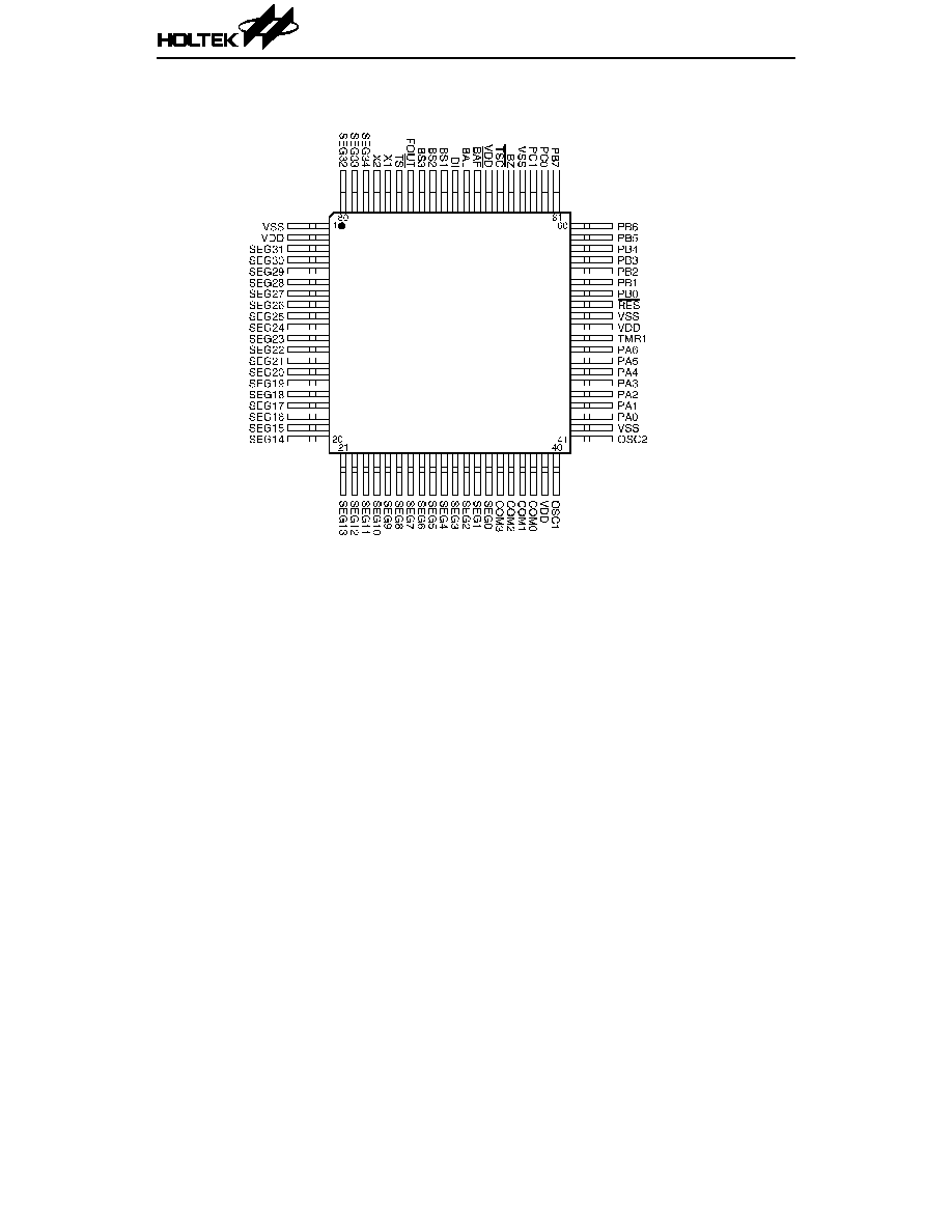
Pin Assignment
HT9480
2
23th Feb '98
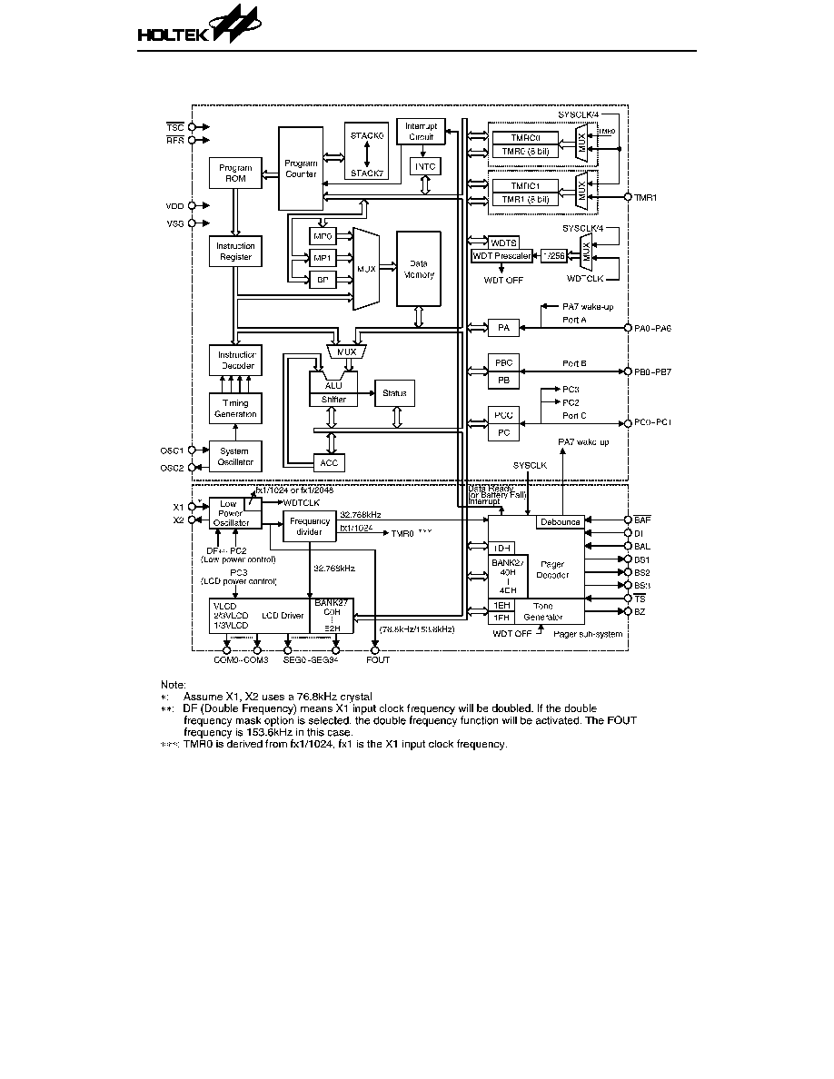
Block Diagram
HT9480
3
23th Feb '98
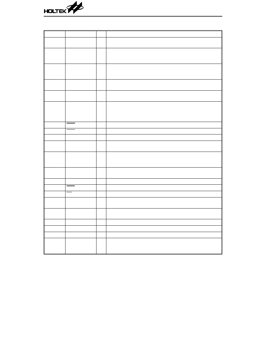
Pin Description
Pin No
Pin Name
I/O
Function
43~49
PA0~PA6
I
7-bit input ports, with pull-high resistors
Each bit can be configured as a wake-up input by mask option.
54~61
PB0~PB7
I/O
Bidirectional 8-bit input/output ports, pull-high mask option
The output structures, whether tri-state or CMOS, are
determined by software instructions.
62~63
PC0~PC1
I/O
Bidirectional 2-bit input/output ports, pull-high mask option
The output structures, whether tri-state or CMOS, are
determined by software instructions.
1, 42,
52, 64
VSS
Negative power supply (GND)
76
77
X1
X2
I
O
X1 and X2 are connected to an external crystal to form an
internal low power oscillator clock.
40
41
OSC1
OSC2
I
O
OSC1 and OSC2 are connected to an RC network or a crystal
(determined by mask option) to form the system clock oscillator.
For RC operation, OSC2 is the output terminal of the system
clock.
53
RES
I
Schmitt trigger reset input, active low
68
BAF
I
Battery fail interrupt with debounce circuit input
50
TMR1
I
Schmitt trigger input for timer/event counter
2, 39, 51
67
VDD
Positive power supply
65
BZ
O
Buzzer non-inverting BZ output
The BZ pin outputs "high" at buzzer off (by setting the value 00H
of 1DH)
3~34
78~80
SEG31~SEG0
SEG34~SEG32
O
LCD driver outputs for LCD panel segments
35~38
COM3~COM0
O
Outputs for LCD panel common connections
66
TSC
I
µ
C test mode input pin, active low with pull-high resistor
75
TS
I
Decoder test mode input pin, active low with a pull-high resistor
69
BAL
I
Battery low indication input, active high without pull-high
resistor
70
DI
I
POCSAG code input serial data (inverting or non-inverting as
determined by SPF32). CMOS input without pull-high resistor
71
BS1
O
Pager receiver power control enable output, CMOS output
72
BS2
O
RF dc level adjustment pin, CMOS output
73
BS3
O
PLL control pin, CMOS output
74
FOUT
O
Frequency reference output pin
The FOUT output pin produces a 76.8kHz/153.6kHz signal with
a 1/2 duty cycle reference frequency if a 76.8kHz crystal is used.
HT9480
4
23th Feb '98
Absolute Maximum Ratings*
Supply Voltage .............................. 0.3V to 5.5V
Storage Temperature................. 50
°
C to 125
°
C
Input Voltage..................V
SS
0.3V to V
DD
+0.3V
Operating Temperature............... 25
°
C to 85
°
C
*Note: Stresses above those listed under "Absolute Maximum Ratings" may cause permanent
damage to the device. These are stress ratings only. Functional operation of this device at
these or any other conditions above those indicated in the operational sections of this
specification is not implied and exposure to absolute maximum rating conditions for extended
periods may affect device reliability.
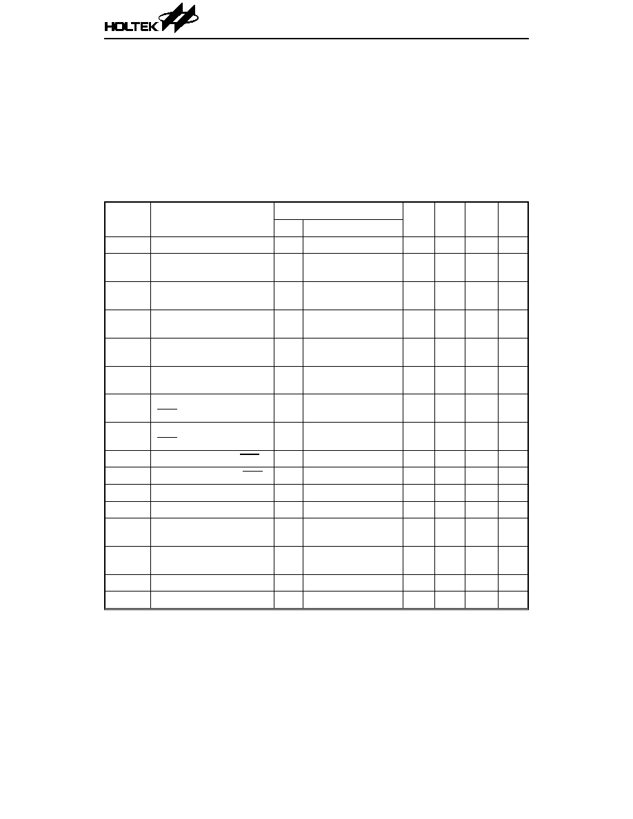
D.C. Characteristics
(Ta=25
°
C)
Symbol
Parameter
Test Conditions
Min.
Typ.
Max.
Unit
V
DD
Conditions
V
DD
Operating Voltage
--
3V application
2.2
3.0
3.5
V
I
DD
Operating Current
3V
No load,
fsys=153.6kHz
--
300
--
µ
A
I
STB1
Standby Current 1
3V
No load, System
HALT (Watchdog ON)
--
200
--
µ
A
I
STB2
Standby Current 2
3V
No load, System
HALT (Watchdog OFF)
--
--
1
µ
A
V
IL
Input Low Voltage for
Input Port and I/O Port
3V
--
0
--
1
V
V
IH
Input High Voltage for
Input Port and I/O Port
3V
--
2.2
--
3
V
V
IL1
Input Low Voltage
(RES,TMR1,BAL)
3V
--
0
--
1
V
V
IH1
Input High Voltage
(RES,TMR1,BAL)
3V
--
2.2
--
3
V
V
IL2
Input Low Voltage (BAF)
3V
--
0
--
0.9
V
V
IH2
Input High Voltage (BAF)
3V
--
1.3
--
3
V
I
OL
I/O Port Sink Current
3V
V
OL
=0.3V
1.7
3.4
--
mA
I
OH
I/O Port Source Current
3V
V
OH
=2.7V
1
1.9
--
mA
I
OL
Segment 0-34 Output
Sink Current
3V
V
OL
=0.3V
20
44
--
µ
A
I
OH
Segment 0-34 Output
Source Current
3V
V
OH
=2.7V
20
38
--
µ
A
I
OL
BZ, Sink Current
3V
V
OL
=0.3V
1
2.5
--
mA
I
OH
BZ, Source Current
3V
V
OH
=2.7V
1
2
--
mA
HT9480
5
23th Feb '98
Document Outline