 | ÐлекÑÑоннÑй компоненÑ: HT82V842 | СкаÑаÑÑ:  PDF PDF  ZIP ZIP |
Äîêóìåíòàöèÿ è îïèñàíèÿ www.docs.chipfind.ru
HT82V842
CCD CDS/PGA/10b-20M-ADC
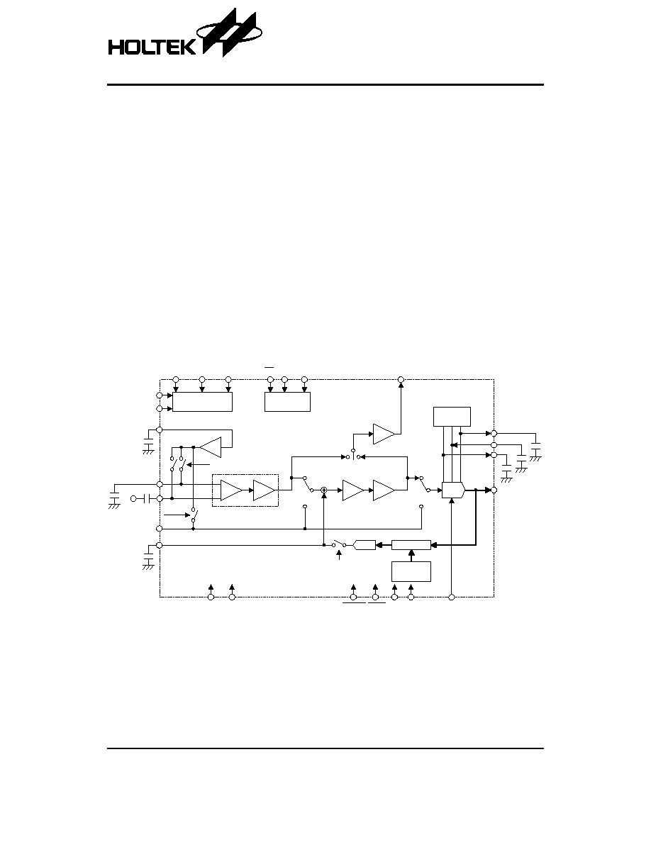
Block Diagram
Rev. 1.00
1
July 15, 2004
Features
·
Operating voltage: 2.7V~3.6V
·
Low power consumption: 70mW (Typ.)
·
Power down mode: less than 30
mW
·
Accepts a direct signal input to ADC or PGA at 1.0
V
PP
(Typ.)
·
CCD signal input level: 1.1 V
P-P
(Max.)
·
10-bit ADC (up to 20MHz)
-
DNL:
±0.6 LSB (Typ.)
·
Black level neutralizer, target setting: 16~127LSB
·
Built-in serial interface
·
Independent ADC input conversion clock and data
output clock
·
Independent CDS and PGA gain control
-
CDS:
-1.94/0/6/12dB
-
PGA: 0~24dB
·
Wide gain range:
-1.94~36dB
·
High speed sample and hold circuit: pulse width 11ns
(Min.)
·
48-pin LQFP package
S / H
C L P C A P
A D I N
T i m i n g
G e n e r a t o r
S e r i a l
R e g i s t e r
O B P C C D C L P A D C L P
C S S C K S D A T A
A D C K
B L K
D C C l a m p
C C D C L P
C C D I N
C C D
R E F I N
A D C L P
O B P
D A C
B a n d G a p
C i r c u i t
C o m p a r e
B l a c k L e v e l
R e g i s t e r
1 0 - B i t
A D C
0 / 6 / 1 2 / 1 8 d B
0 ~ 6 d B
( 0 . 0 4 7 d B / S t e p )
P G A
R o u g h
P G A
F i n e
C D S
- 1 . 9 4 / 0 / 6 / 1 2 d B
O B C A P
M O N O U T
V
D D
V
S S
R E S E T S T B Y S H R S H D
O U T C K
V R N
V C O M
V R P
D O 0 ~ D O 9
General Description
The HT82V842 is a CMOS single-chip signal process-
ing device for CCD area sensors. It consists of a clamp
circuit, Correlated Double Sampler (CDS), Programma-
ble Gain Amplifier (PGA), reference voltage generator,
black level detection circuit, 20MHz 10-bit A/D converter
(ADC), timing generator for internally required pulses,
serial interface for internal function control and PGA
gain control.
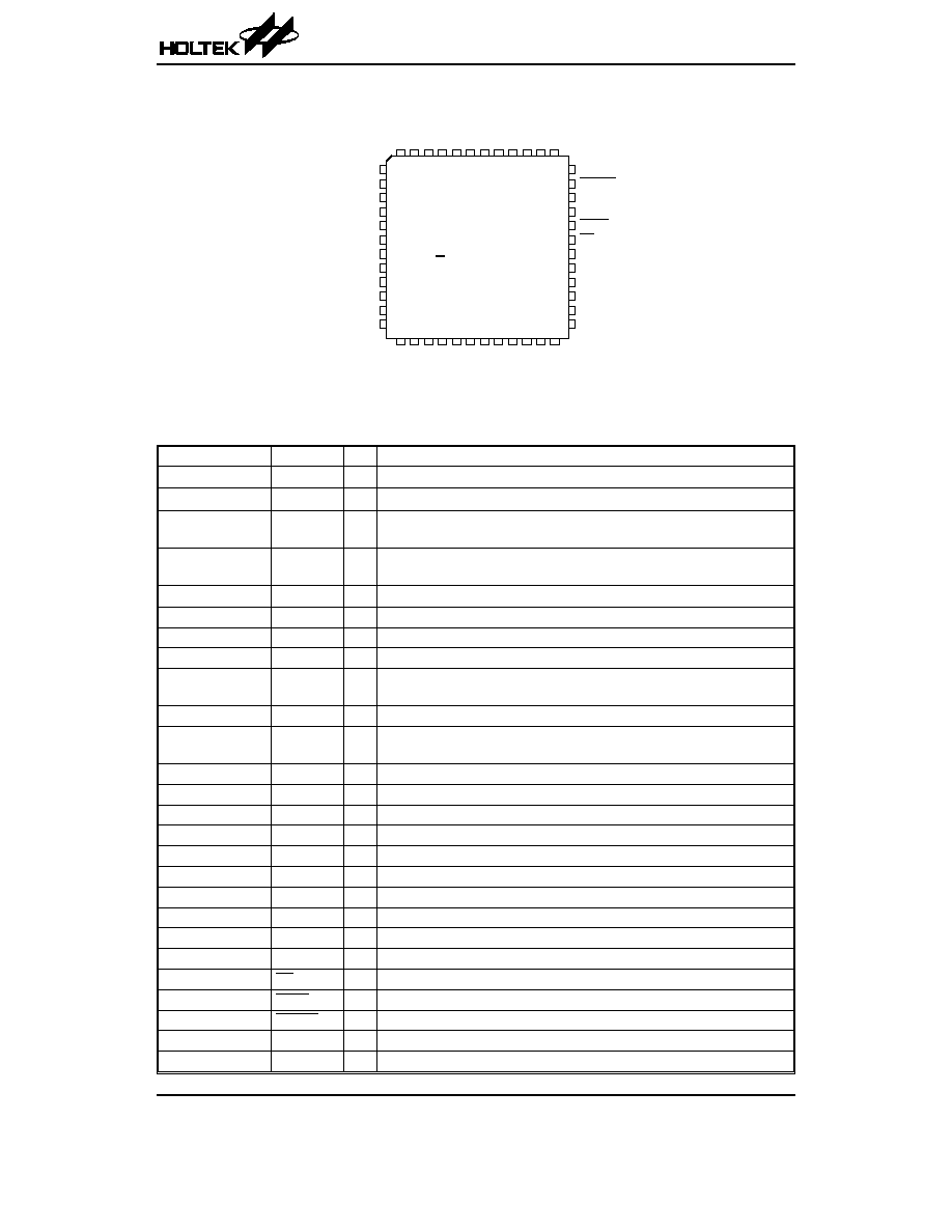
Pin Assignment
Pin Description
Pin No.
Pin Name
I/O
Description
1, 3, 17~18, 21
NC
¾ No connection
2, 6~7, 19, 34, 43
VDD
¾ Positive power supply for analog circuit
4
VRN
O
Negative reference voltage for internal ADC
Connect to V
SS
via 0.1
mF
5
VRP
O
Positive reference voltage for internal ADC
Connect to V
SS
via 0.1
mF
8~9, 20, 33, 42
VSS
¾ Negative power supply for analog circuit
10
VCOM
O
Common reference voltage for internal ADC
11
CCDIN
I
CDS circuit data input
12
REFIN
I
CDS circuit reference input
13
CLPCAP
O
Clamp level output
Connect to V
SS
via 0.1
mF
14
ADIN
I
ADIN signal input
15
OBCAP
O
Black level integration voltage
Connect to V
SS
via 0.1
mF~1mF (by applications)
16
MONOUT
O
Monitor output of CDS or PGA
22
ADCK
I
ADC sampling clock input
23
SHR
I
Reference sampling pulse input
24
SHD
I
Data sampling pulse input
25
ADCLP
I
Pulse input for ADIN clamp and black calibration control
26
BLK
I
Blanking pulse input
27
CCDCLP
I
Clamp control input
28
OBP
I
Black level period pulse input
29
SCK
I
Serial clock input
30
SDATA
I
Serial data input
31
CS
I
Serial port chip selection (Active at low)
32
STBY
I
Power down control (Active low)
35
RESET
I
Reset signal (Active low)
36
OUTCK
I
Clock source for ADC output
37~41, 44~48
DO0~DO9
O
Digital output from ADC
HT82V842
Rev. 1.00
2
July 15, 2004
H T 8 2 V 8 4 2
4 8 L Q F P - A
1 3 1 4 1 5 1 6 1 7 1 8 1 9 2 0 2 1 2 2 2 3 2 4
4 8 4 7 4 6 4 5 4 4 4 3 4 2 4 1 4 0 3 9 3 8 3 7
1
2
3
4
5
6
7
8
9
1 0
1 1
1 2
3 6
3 5
3 4
3 3
3 2
3 1
3 0
2 9
2 8
2 7
2 6
2 5
N C
V D D
N C
V R N
V R P
V D D
V D D
V S S
V S S
V C O M
C C D I N
R E F I N
S
H
D
S
H
R
A
D
C
K
N
C
V
S
S
V
D
D
N
C
N
C
M
O
N
O
U
T
O
B
C
A
P
A
D
I
N
C
L
P
C
A
P
O U T C K
R E S E T
V D D
V S S
S T B Y
C S
S D A T A
S C K
O B P
C C D C L P
B L K
A D C L P
D
O
0
D
O
1
D
O
2
D
O
3
D
O
4
V
S
S
V
D
D
D
O
5
D
O
6
D
O
7
D
O
8
D
O
9
Absolute Maximum Ratings
Supply Voltage .........................GND
-0.3V to GND+6V
Storage Temperature ...........................
-55°C to 150°C
Input Voltage .............................V
SS
-0.3V to V
DD
+0.3V
Operating Temperature ..........................
-20°C to 70°C
Note: These are stress ratings only. Stresses exceeding the range specified under
²Absolute Maximum Ratings² may
cause substantial damage to the device. Functional operation of this device at other conditions beyond those
listed in the specification is not implied and prolonged exposure to extreme conditions may affect device reliabil-
ity.
D.C. Characteristics
Ta=25
°C
Symbol
Parameter
Test Conditions
Min.
Typ.
Max.
Unit
V
DD
Conditions
V
IH
High Level Input Voltage
3V
¾
0.7V
DD
¾
V
DD
V
V
IL
Low Level Input Voltage
3V
¾
0
¾
0.3V
DD
V
I
IH
High Level Input Current
3V
V
IL
=0V
¾
¾
200
mA
I
IL
Low Level Input Current
3V
V
IH
=3.0V
¾
¾
1
mA
I
MD
Operation Current at Monitor Disable
3V
f
S
=20MHz
¾
23
¾
mA
I
MA
Supply Current at Monitor Active
3V
f
S
=20MHz
¾
26
¾
mA
I
SS
Power Down Current
3V
¾
¾
¾
10
mA
V
CCDIN
Analog Input Range
3V
CCDIN input,
f
IN
=1MHz
¾
1.1
¾
V
P-P
V
ADIN
3V
ADIN input,
f
IN
=1MHz
¾
1.0
¾
V
P-P
V
CLPCAP
Clamp Voltage
3V
¾
1.5
1.7
1.9
V
t
BLKCAL
Black Calibration Time
3V
¾
¾
¾
200
Pixel
V
BLKCAL
Maximum Calibration Offset Voltage
3V
¾
¾
±200
¾
mV
G (0)
CDS Gain (Set 0 dB)
3V
Absolute gain
-2
-1
0
dB
G (1)
CDS Gain (Set 6.02 dB)
3V
Relative gain
5.52
6.02
6.52
dB
G (2)
CDS Gain (Set 12.04 dB)
3V
11.54
12.04
12.04
dB
G (3)
CDS Gain (Set
-1.94 dB)
3V
-2.44
-1.94
-1.44
dB
Gmin
PGA Gain (Minimum Gain)
3V
Absolute gain
-1.2
-0.2
0.8
dB
Gmax
PGA Gain (Maximum Gain)
3V
Relative gain
22.906
23.906
24.906
dB
Gstep
PGA Gain (Gain Step)
3V
0
0.047
0.094
dB
ER
PA
Total (CDS+PGA) Gain Monotony
3V
¾
¾
¾
±4
LSB
RES
Resolution
3V
¾
¾
¾
10
Bits
DNL
Differential Nonlinearity
3V
f
S
=20MHz
¾
±0.6
±1.0
LSB
SN
S/N
3V
¾
¾
58
¾
dB
SND
S/(N+D)
3V
¾
¾
56
¾
dB
V
COM
ADC Common Voltage
3V
¾
1.25
1.4
1.55
V
V
RP
V
RP
Voltage (Positive)
3V
¾
1.55
1.65
1.75
V
V
RN
V
RN
Voltage (Negative)
3V
¾
1.05
1.15
1.25
V
HT82V842
Rev. 1.00
3
July 15, 2004
Symbol
Parameter
Test Conditions
Min.
Typ.
Max.
Unit
V
DD
Conditions
C
CAL
ADC Output Black Level Calibration Code
3V
¾
16
¾
127
LSB
1
¾
127
LSB
ST
CAL
Calibration Code Resolution
3V
¾
¾
1
¾
LSB
Note:
Black calibration period is specified when C
CAL
is from 16 to 127LSB. Although black level codes of 1 to 15
could be set, t
BLKCAL
is not guaranteed for these codes.
A.C. Characteristics
V
SS
=0V, Ta=25
°C
Symbol
Parameter
Test Conditions
Min.
Typ.
Max.
Unit
V
DD
Conditions
f
S
Conversion Frequency
3.0V
¾
0.5
¾
20
MHz
t
CYC
Clock Cycle Time
3.0V
¾
50
¾
¾
ns
t
R
Clock Rising Time
3.0V
¾
¾
¾
2
ns
t
F
Clock Falling Time
3.0V
¾
¾
¾
2
ns
t
L
Clock Low Period
3.0V
¾
23
¾
¾
ns
t
H
Clock High Period
3.0V
¾
23
¾
¾
ns
t
WR
SHR Pulse Width
3.0V
¾
11
¾
¾
ns
t
WD
SHD Pulse Width
3.0V
¾
11
¾
¾
ns
t
DR
SHR Sampling Aperture
3.0V
¾
¾
¾
4
ns
t
DD
SHD Sampling Aperture
3.0V
¾
¾
¾
4
ns
t
PSUP
Data Pulse Setup
3.0V
¾
2
¾
¾
ns
t
HOLD
Data Pulse Hold
3.0V
¾
5
¾
¾
ns
t
SP
Sampling Pulse Non-overlay
3.0V
¾
1
¾
¾
ns
t
SUPE
Enable Pulse Setup
3.0V
¾
10
¾
¾
ns
t
HOLDE
Enable Pulse Hold
3.0V
¾
10
¾
¾
ns
t
SUPOC
OUTCK Setup
3.0V
¾
0
¾
¾
ns
t
HOLDOC
OUTCK Hold
3.0V
¾
10
¾
¾
ns
t
DLD
3-state Disable Delay
3.0V Active
® High-Z
¾
20
¾
ns
t
DLE
3-state Disable Delay
3.0V High-Z
® Active
¾
20
¾
ns
t
DL
ADC Output Data Delay
3.0V
¾
¾
6
¾
ns
HT82V842
Rev. 1.00
4
July 15, 2004
HT82V842
Rev. 1.00
5
July 15, 2004
Functional Description
CDS (Correlated Double Sampling) Circuit
Connect the CCDIN pin to the CCD sensor thru a capac-
itor. Connect also the REFIN pin to V
SS
thru a capacitor.
The CDS circuit holds the pre-charge voltage of the
CCD at SHR pulse and do sampling of the CCD pixel
data at SHD pulse. Correlated noise is removed by sub-
tracting the pre-charge voltage from the pixel data level.
CDS could choose a gain setting from 0, 6.02, 12 or
-1.94dB (Mode 3, register D4 and D5 bits). A CDS gain
is controlled by PGA gain. It is recommended to in-
crease the CDS gain then increase the PGA gain to re-
duce the noise level.
Clamp Circuits
·
DC clamp
The DC level of the CCDIN/REFIN input is fixed by an
internal DC clamp circuit. The DC level of the
C-coupled CCD signal at the CDS input is set to
CLPCAP by the internal DC clamp circuit. The clamp
switches are usually turned on at the black level cali-
bration period. The CLPCAP pin connects to V
SS
thru
a 0.1
mF capacitor.
·
ADIN signal clamp
Clamp operation can also be used for the ADIN path.
The clamp voltage is different from the CCDIN/REFIN
signal and it could be turned off by register setting. At
²ADIN signal to ADC² mode, the ADCLP signal con-
trols the
²clamp circuit². Black level calibration circuit
is also controlled by ADCLP at
²ADIN signal to PGA²
mode.
·
Clamp control
¨
Clamp current (Mode 2 register D7). Charge current
can select normal or fast clamp.
¨
Clamp target (Mode 2 register D5 and D4), input
signals (REFIN and CCDIN) to be clamped are
selectable. The clamp function can be turned off.
Black Level Cancel Circuit
The purpose of a black level cancel circuit is to control
the DC level of the PGA input. The ADC output code at
an optical black period may correspond to the black
level code set up by the register. A black level code of (1
to) 16 to 127 LSB is available (the default is 64 LSB).
While the OBP pin is active a black level cancel loop is
established. In the loop, a comparison is made between
the ADC output code and the black level code, the result
controls the voltage of the OBCAP capacitor. Hence, the
OBCAP voltage settles gradually and the signal level of
the optical black period corresponds to the established
value.
The following conditions will reset the OBCAP capaci-
tor:
·
Set the black level reset register to
²1² (Mode 1 regis-
ter D1=1).
·
Set the RESET pin to low
·
Power down by STBY pin or register control
The DC clamping (CCDCLP) is allowed while the OBP
pin is low. The black level cancellation is available at
²ADIN signal to PGA² mode. The black level cancella-
tion is available at the ADCLP period in this mode. The
clamping function and black level canceling function are
done simultaneously.
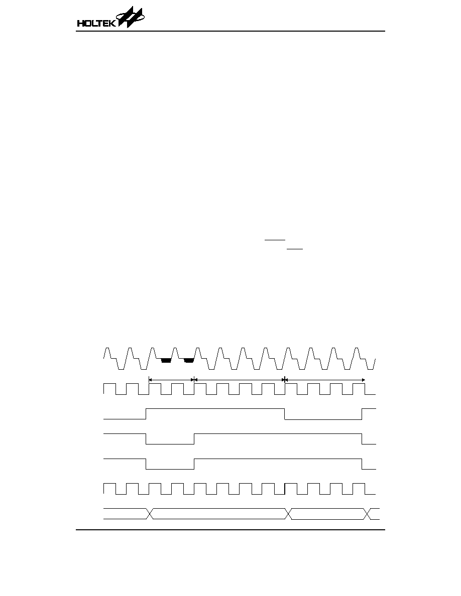
D a t a O u t p u t
O B
E f f e c t i v e P i x e l
C C D
A D C K
B L K
O B P
C C D C L P
O U T C K
D O
0
~ D O
9
B l a c k C o d e
B l a n k i n g
Document Outline
- þÿ
- þÿ
- þÿ
- þÿ
- þÿ
- þÿ
- þÿ
- þÿ
- þÿ
- þÿ
- þÿ