 | ÐлекÑÑоннÑй компоненÑ: HT82M980A | СкаÑаÑÑ:  PDF PDF  ZIP ZIP |
Äîêóìåíòàöèÿ è îïèñàíèÿ www.docs.chipfind.ru
HT82M980A
5-Key 3D WIN2000 USB+PS/2 Mouse Controller
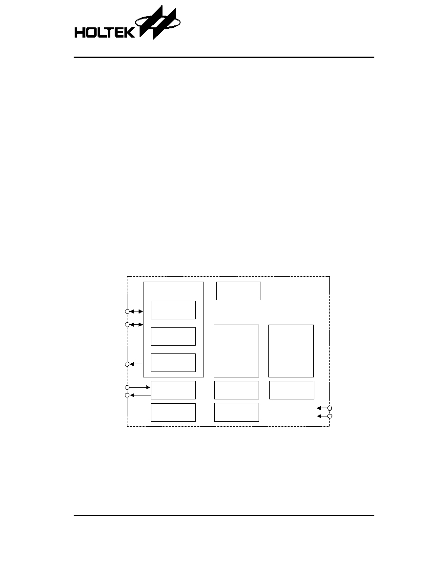
Block Diagram
Rev. 1.40
1
February 10, 2003
Features
·
Operating voltage: 4.4V~5.25V
·
Compatible with Microsoft Windows 2000 and
5-button Wheel Mouse
·
Complete Universal Serial Bus specs V1.1
compatibility
·
Serial Bus Interface Engine (SIE)
·
USB transceiver
·
Microsoft 3D Intelli mouse and IBM PS/2 mouse
compatible
·
Supports five buttons and three axes input
·
Z axis can support two kinds of scroller input
(optomechanical and mechanical)
·
Single chip solution especially for USB mouse
function
·
HALT function and wake-up feature reduce power
consumption
·
Plug and Play functions
·
Minimal external components
·
6MHz crystal oscillator for system clock
·
20-pin DIP package
General Description
HT82M980A is a Plug and Play Windows 2000 and
5-button 3D USB+PS/2 Mouse controller. The
HT82M980A can support the USB Standard Request as
well as HID Class Request version 1.1. It is compatible
with Microsoft Intelli 3D PS/2 mouse. The X/Y axis photo
input with built-in Holtek
¢s special dynamic photo-input
resistor and Z axis can support two kinds of scroller in-
put, namely; mechanical and optomechanical. It re-
quires minimal external components to implement 3D
USB plus PS/2 mouse. All its features combined and
make up this versatile Holtek 8-bit MCU with an on-chip
USB interface logic. The USB is specified by the
Univer-
sal Serial Bus Specification V1.1.
U S B
T r a n s c e i v e r
U S B
R e c e i v e r
U S B
T r a n s m i t t e r
V o l t a g e
R e g u l a t o r
C l o c k
G e n e r a t o r
R C
R E S E T
R e g i s t e r
S e t
M a i n
S t a t e m a c h i n e
S u s p e n s i o n
C o n t r o l
U S B S e r i a l
I n t e r f a c e E n g i n e
( S I E )
a n d
C o n t r o l
L o g i c
H o l t e k
8 - b i t
M i c r o c o n t r o l l e r
F I F O s ´ 2
U S B D +
U S B D -
V 3 3 O
O S C 1
O S C 2
V D D
V S S
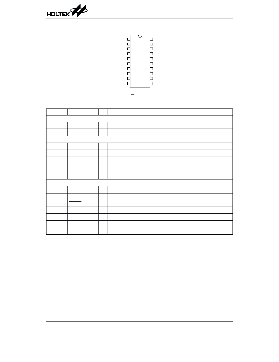
Pin Assignment
Pin Description
Pin No.
Pin Name
I/O
Description
USB Interface (2 pins)
3
USBD+/CLK
I/O
USB data plus or PS2 Clock, F/W auto-detect USBD+ for USB, CLK for PS2
4
USBD
-/DATA
I/O
USB data minus or PS2 Data, F/W auto-detect USB
- for USB, DATA for PS2
General purpose I/O (11 pins)
6, 7
X1, X2
I
X-axis photo input with built-in Holtek
¢s special dynamic photo input resistor
8, 9
Y1, Y2
I
Y-axis photo input with built-in Holtek
¢s special dynamic photo input resistor
12, 13
Z1, Z2
I
Z-axis input supports two kinds of scroller input; optomechanical and me-
chanical
10, 11, 14
15, 16
L, R, M, B4, B5
I
Input ports with pull-high resistor. These pads can function as Left, Right, Mid-
dle, B4 and B5 button input lines.
Miscellaneous (7 pins)
1
VSS
¾ Negative power supply, ground
2
V33O
O
3.3V voltage output
5
RESET
I
Chip reset input, low active
17
LED
I/O
Drives LED output
18
VDD
¾ 5V positive power supply
19
OSC2
O
6MHz OSC output
20
OSC1
I
6MHz OSC input
Absolute Maximum Ratings
Supply Voltage ............................................
-0.3V to 6V
Storage Temperature ............................
-50°C to 125°C
MCU Input Voltage.....................V
SS
-0.3V to V
DD
+0.3V
Operating Temperature...........................
-25°C to 70°C
USB Input Voltage ....................V
SS
-0.3V to V
33O
+0.3V
Note: These are stress ratings only. Stresses exceeding the range specified under
²Absolute Maximum Ratings² may
cause substantial damage to the device. Functional operation of this device at other conditions beyond those
listed in the specification is not implied and prolonged exposure to extreme conditions may affect device reliabil-
ity.
HT82M980A
Rev. 1.40
2
February 10, 2003
V S S
V 3 3 O
U S B D + / C L K
U S B D - / D A T A
R E S E T
X 1
X 2
Y 1
Y 2
B 4
O S C 1
O S C 2
V D D
L E D
M
R
L
Z 2
Z 1
B 5
H T 8 2 M 9 8 0 A
2 0 D I P - A
2 0
1 9
1 8
1 7
1 6
1 5
1 4
1 3
1 2
1 1
1
2
3
4
5
6
7
8
9
1 0
D.C. Characteristics
Ta=25
°C
Symbol
Parameter
Test Conditions
Min.
Typ.
Max.
Unit
V
DD
Conditions
V
DD
Operating Voltage
¾
¾
4.4
¾
5.25
V
I
DD
Operating Current
(Crystal OSC)
5V
No load,
f
SYS
=6MHz
USB mode
¾
10
¾
mA
PS/2 mode
¾
3
¾
mA
I
SUS
USB Suspend Mode
5V
No load, system HALT
¾
¾
250
mA
V
IL1
Input Low Voltage
(X1, X2, Y1, Y2, Z1, Z2, L, M,
R, B4, B5)
5V
¾
0
¾
1.0
V
V
IH1
Input High Voltage
(X1, X2, Y1, Y2, Z1, Z2, L, M,
R, B4, B5)
5V
¾
3.5
¾
5
V
V
IL2
Input Low Voltage
(RESET)
5V
¾
0
¾
1.5
V
V
IH2
Input High Voltage
(RESET)
5V
¾
3.5
¾
5
V
V
POR
Built-in Power on Reset V
DD
Detection Voltage
5V
¾
¾
3.7
¾
V
I
OL
Sink Current (LED)
5V
V
OL
=0.8V
¾
50
¾
mA
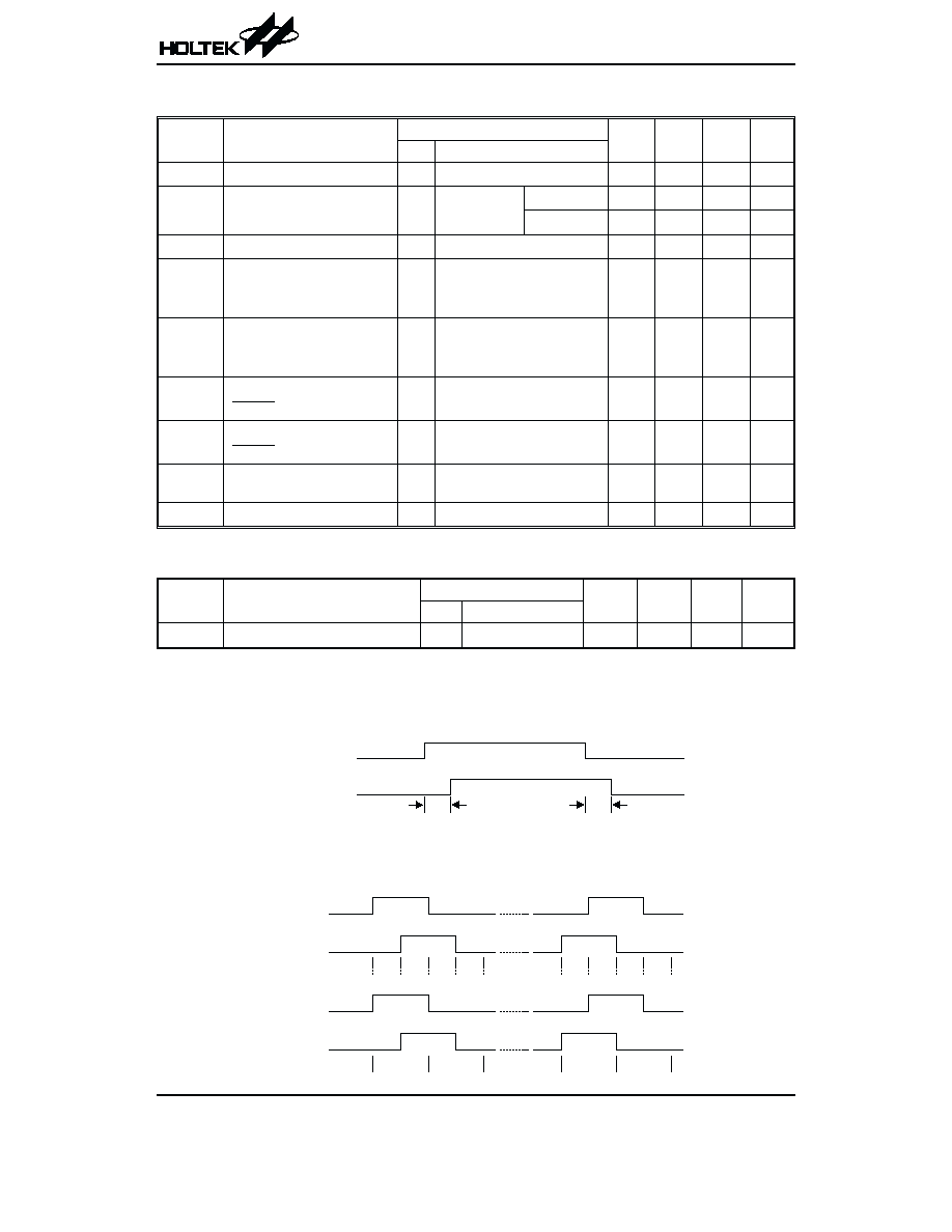
A.C. Characteristics
Ta=25
°C
Symbol
Parameter
Test Conditions
Min.
Typ.
Max.
Unit
V
DD
Conditions
f
SYS
System Clock (Crystal OSC)
5V
¾
0
6000
¾
kHz
Note: t
SYS
=1/f
SYS
Timing Diagram
X, Y Axis Photo-Coupler Crossed Width
X, Y, Z Axis Counting
HT82M980A
Rev. 1.40
3
February 10, 2003
X 1 ( Y 1 ) ( Z 1 )
X 2 ( Y 2 ) ( Z 2 )
t
r
t
f
t
p
N o t e : . o r X , Y - a x i s t
r
, t
p
, t
f
> 3 0 m s
. o r Z - a x i s t
r
, t
p
, t
f
> 1 m s
X 1
X 2
+ 1
+ 1
+ 1
+ 1
- 1
- 1
- 1
- 1
Z 1
Z 2
+ 1
+ 1
- 1
- 1
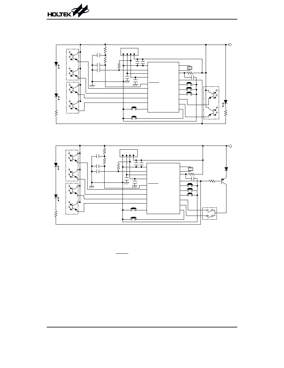
Application Circuits
This Application Circuit is for Reference Only
Note:
Layout 0.1
mF capacitor, 22W resistor and 0.01mF capacitor as close to VDD pin as possible.
Layout power plane and ground plane as large as possible.
Place 0.1
mF capacitor as close to RESET pin as possible.
Place 6MHz crystal as close to OSC1 and OSC2 pins as possible.
Components with * are used for EMC issue.
HT82M980A
Rev. 1.40
4
February 10, 2003
H T 8 2 M 9 8 0 A
6 M H z
1 k W
V
D D
R E C E P T _ A
1
2
3
4
1 . 5 k W
0 . 1 m .
1 k W
1 0 m .
0 . 0 1 m . *
0 . 1 m .
2 0
1 9
1 8
1 7
1 6
1 5
1 4
1 3
1 2
1 1
2 2 W *
1
2
3
4
5
6
7
8
9
1 0
V S S
V 3 3 O
U S B D + / C L K
U S B D - / D A T A
R E S E T
X 1
X 2
Y 1
Y 2
B 4
O S C 1
O S C 2
V D D
L E D
M
R
L
Z 2
Z 1
B 5
3 3 p . *
3 3 p . *
2 . 2 m .
1 M W
0 . 1 m . *
1 0 k W *
6 M H z
V
D D
R E C E P T _ A
1
2
3
4
1 . 5 k W
0 . 1 m .
1 k W
Z - a x i s M e c h n i c a l
E n c o d e r
1 0 k W
1 0 m .
0 . 0 1 m . *
H T 8 2 M 9 8 0 A
0 . 1 m .
2 2 W *
2 0
1 9
1 8
1 7
1 6
1 5
1 4
1 3
1 2
1 1
1
2
3
4
5
6
7
8
9
1 0
V S S
V 3 3 O
U S B D + / C L K
U S B D - / D A T A
R E S E T
X 1
X 2
Y 1
Y 2
B 4
O S C 1
O S C 2
V D D
L E D
M
R
L
Z 2
Z 1
B 5
3 3 p . *
3 3 p . *
2 . 2 m .
1 M W
0 . 1 m . *
1 0 k W *
Package Information
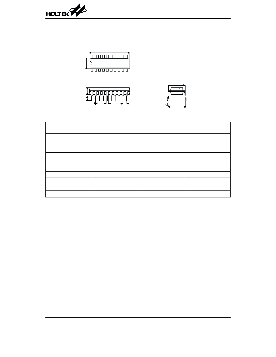
20-pin DIP (300mil) Outline Dimensions
Symbol
Dimensions in mil
Min.
Nom.
Max.
A
1020
¾
1045
B
240
¾
260
C
125
¾
135
D
125
¾
145
E
16
¾
20
F
50
¾
70
G
¾
100
¾
H
295
¾
315
I
335
¾
375
a
0
°
¾
15
°
HT82M980A
Rev. 1.40
5
February 10, 2003
2 0
1
1 1
1 0
a
A
B
C
D
E
.
G
H
I
Document Outline
- þÿ
- þÿ
- þÿ
- þÿ
- þÿ
- þÿ
- þÿ
- þÿ
- þÿ
- þÿ
- þÿ