 | ÐлекÑÑоннÑй компоненÑ: HT82M938R | СкаÑаÑÑ:  PDF PDF  ZIP ZIP |
Äîêóìåíòàöèÿ è îïèñàíèÿ www.docs.chipfind.ru
HT82M938T/HT82M938R
27MHz 3D PS2 Mouse Controller
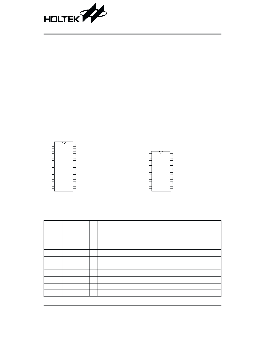
Pin Assignment
Pin Description
Transmitter
Pin No.
Pin Name
I/O
Description
1, 20
Z1, Z2
I
Z-axis input supports two kinds of scroller input; optomechanical and mechani-
cal.
2, 3, 4, 5, 6 R, M, L, B4, B5
I
Input ports with pull-high 12k
W resistor. These pads can function as Left, Right,
Middle, B4 and B5 button lines.
7
VSS
¾ Negative power supply, ground
9, 10
X, X2
I
X-axis photo input
11, 12
Y1, Y2
I
Y-axis photo input
13
RESET
I
Chip reset input, low active
14
VDD
¾ 5V positive power supply
15
OSC1
I
6MHz OSC input
16
OSC2
O
6MHz OSC output
Rev. 1.30
1
October 29, 2002
Features
·
Compatible with Microsoft Windows 2000 and
5-Button Wheel Mouse
·
Compatible with Microsoft Intelli 3D PS/2 and IBM
PS/2 mouse compatible
·
Supports rolling buttons in 3D PS/2 mouse mode
·
Supports five buttons (R,M,L,B4,B5) and three axes
( X,Y,Z)input
·
Z axis can support optomechanical and mechanical
scroller input
·
Crystal oscillator system frequency 6MHz for trans-
mitter and 6MHz for receiver
·
27MHz Single Channel with 8 ID Code
·
Transmitter 20-pin SOP and receiver 16-pin SOP
package
General Description
The HT82M938T/HT82M938R is a Plug & Play 27MHz
RF 5 Buttons 3D PS/2 mouse controller transmitter and
receiver. It is compatible with Microsoft Intelli 3D PS/2
Wheel Mouse. The operation of the Z axis can support
optomechanical and mechanical scroller input.
1 6
1 5
1 4
1 3
1 2
1 1
1 0
9
1
2
3
4
5
6
7
8
2 0
1 9
1 8
1 7
1 6
1 5
1 4
1 3
1 2
1 1
1
2
3
4
5
6
7
8
9
1 0
Z 1
R
M
L
B 4
B 5
V S S
N C
X 1
X 2
Z 2
I R _ O N
R . _ O U T
R . _ E N
O S C 2
O S C 1
V D D
R E S E T
Y 2
Y 1
N C
D A T A
N C
N C
N C
V S S
N C
C L K
N C
L E D
R E S _ C H
O S C 2
O S C 1
V D D
R E S E T
R . _ I N
H T 8 2 M 9 3 8 T
2 0 S O P - A
H T 8 2 M 9 3 8 R
1 6 S O P - A
T r a n s m i t t e r
R e c e i v e r
Pin No.
Pin Name
I/O
Description
17
RF_EN
O
RF module enable
18
RF_OUT
O
RF data output
19
IR_ON
O
X, Y, Z photo input power control
Receiver
Pin No.
Pin Name
I/O
Description
2
DATA
I/O
PS/2 mouse
²DATA² line with pull-high 12kW resistor
6
VSS
¾ Negative power supply, ground
8
CLK
I/O
PS/2 mouse
²CLOCK² line with pull-high 12kW resistor
9
RF_IN
I
RF data input
10
RESET
I
Chip reset input, low active
11
VDD
¾ 5V positive power supply
12
OSC1
I
6MHz OSC input
13
OSC2
O
6MHz OSC output
14
RES_CH
I
Channel select reset switch with pull-high 12k
W resistor
15
LED
O
Data transfer and change channel mode display LED
Electrical Characteristics
Transmitter
Symbol
Parameter
Test Conditions
Min.
Typ.
Max.
Unit
V
DD
Conditions
V
DD
Operating Voltage
¾
¾
2.4
¾
5.5
V
I
DD
Operating Current (Crystal OSC)
3V
No load, f
SYS
=6MHz
¾
0.7
1.5
mA
I
STB
Standby Current
3V
No load, system HALT
¾
¾
8
mA
V
IL
Input Low Voltage (X1, X2, Y1, Y2,
Z1, Z2, R, M, L, B4, B5)
3V
¾
0
¾
1
V
V
IH
Input High Voltage (X1, X2, Y1, Y2,
Z1, Z2, R, M, L, B4, B5)
3V
¾
2.1
¾
3
V
V
IL1
Input Low Voltage (RESET)
3V
¾
0
¾
0.7
V
V
IH1
Input High Voltage (RESET)
3V
¾
2.5
¾
3
V
Receiver
Symbol
Parameter
Test Conditions
Min.
Typ.
Max.
Unit
V
DD
Conditions
V
DD
Operating Voltage
¾
¾
2.4
¾
5.5
V
I
DD
Operating Current (Crystal OSC)
5V
No load, f
SYS
=6MHz
¾
2
5
mA
I
STB
Standby Current
5V
No load, system HALT
¾
¾
15
mA
V
IL
Input Low Voltage (RES_CH)
5V
¾
0
¾
1.5
V
V
IH
Input High Voltage (RES_CH)
5V
¾
3.5
¾
5
V
V
IL1
Input Low Voltage (RESET)
5V
¾
0
¾
1.3
V
V
IH1
Input High Voltage (RESET)
5V
¾
4.1
¾
5
V
HT82M938T/HT82M938R
Rev. 1.30
2
October 29, 2002
HT82M938T/HT82M938R
Rev. 1.30
3
October 29, 2002
Functional Description
Change ID procedure
·
First press Receiver RESET key, the LED will blink
very quickly.
·
Now press Transmitter L, M, R button at least
3-minutes, the mouse will jump to change ID mode
and output a change ID signal to the receiver.
·
At the same time, the LED of the Receiver will blink
slowly to wait the change ID information.
·
The user can decide which ID to be changed by press-
ing M button. If the user wants to change ID to 4, just
press the M button four time (This mouse support 8
ID).
·
After deciding the ID number, the user can easy return
to normal mode by pressing the L or R button once.
·
After the Receiver receive the END signal of the
change ID, the LED will no longer blink and the Re-
ceiver returns to normal mode.
PS/2 mouse
·
PS/2 status byte
Bit
7:
RESERVED
6:
0=STREAM MODE, 1=REMOTE MODE
5:
0=DISABLED, 1=ENABLED
4:
0=SCALING 1:1, 1=SCALING 2:1
3:
RESERVED
2:
1=LEFT BUTTON PRESSED
1:
1=MIDDLE BUTTON PRESSED
0:
1=RIGHT BUTTON PRESSED
·
Standard PS/2 data format
Variable rps, 0, 8, 1, bidirectional synchronous.
Bit No.
7
6
5
4
3
2
1
0
1st word
YV
XV
YS
XS
1
M
R
L
2nd word
X7
X6
X5
X4
X3
X2
X1
X0
3rd word
Y7
Y6
Y5
Y4
Y3
Y2
Y1
Y0
·
Data format for 3D PS/2
Variable rps, 0, 8, 1, bidirectional synchronous.
Bit No.
7
6
5
4
3
2
1
0
1st word
YV
XV
YS
XS
1
M
R
L
2nd word
X7
X6
X5
X4
X3
X2
X1
X0
3rd word
Y7
Y6
Y5
Y4
Y3
Y2
Y1
Y0
4th word
Z7
Z6
Z5
Z4
Z3
Z2
Z1
Z0
Note:
The X/Y data report is 9-bit 2
¢s complement
The Z data report is 8-bit 2
¢s complement
X movement towards the right is positive,
movement towards the left is negative
Y upward movement is positive, moving down
is negative
Z rolling towards the user is positive, else nega-
tive
Button status: 1=pressed, 0=released
·
Mouse mode changes between standard and 3D
PS/2 mode
¨
Sending the commands in the following sequence
will set the mouse to 3D PS/2 mode.
Command
Response from mouse
F3h
FAh
C8h
FAh
F3h
FAh
64h
FAh
F3h
FAh
50h
FAh
F2h
Fah
¨
Any time the PC sends a reset
¢FFh¢ command to
the mouse, it will reset the mouse to standard PS/2
mode.
¨
After power-on reset is initiated, the mouse is set to
standard PS/2 mode.
5-button wheel mouse mode follows the 5-button acti-
vation method of Windows 2000 and 5-button wheel
mouse specification.
Timing Diagrams
X, Y, Z input
·
X, Y Axis photo-coupler cross width
For X, Y-axis t
R
, t
F
>100
ms; For Z-axis t
R
, t
F
>1ms
·
X/Y/Z Axis counting
PS/2 mouse
·
Data output
Timing Parameter
Min/Max
T1
Data transition to the falling edge of CLOCK
5/25
msec
T2
Rising edge of CLOCK to DATA transition
5/T4-5
msec
T3
Duration of CLOCK low
30/50
msec
T4
Duration of CLOCK high
30/50
msec
T5
Minimum time to MOUSE inhibit after clock 11
>0
msec
T6
Maximum time to MOUSE inhibit after clock 11 to ensure MOUSE does not start
another transmission
<50
msec
HT82M938T/HT82M938R
Rev. 1.30
4
October 29, 2002
X 1 ( Y 1 ) ( Z 1 )
X 2 ( Y 2 ) ( Z 2 )
t
R
t
.
X 1
X 2
+ 1
+ 1
+ 1
+ 1
+ 1
+ 1
+ 1
+ 1
Z 1
Z 2
+ 1
+ 1
- 1
- 1
( 1 )
( 3 )
( 3 )
( 3 )
( 3 )
( 4 )
S t o p B i t
T 5
( 5 )
( 7 )
1 1 t h
C L K
T 6
1 0 t h
C L K
P a r i t y B i t
B i t 0
T 1
S t a r t B i t
T 2
T 3
T 4
( 2 )
D A T A
C L K
2 n d
C L K
·
Data input
Timing Parameter
Min/Max
T7
Duration of CLOCK low
30/50
msec
T8
Duration of CLOCK high
30/50
msec
T9
Time from low to high CLOCK transition to time when MOUSE samples DATA line
5/25
msec
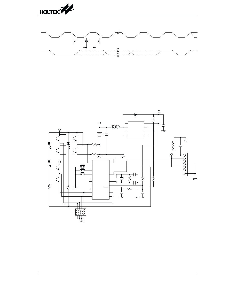
Application Circuits
Transmitter application (This application circuit is for reference only)
Note:
* 10
W is placed if HT7627 is used to reset HT82M938T
HT82M938T/HT82M938R
Rev. 1.30
5
October 29, 2002
( 1 )
( 2 )
9 t h
C L K
P a r i t y B i t
B i t 0
S t a r t B i t
D A T A
C L K
1 s t
C L K
( 3 )
M o u s e
I n h i b i t
2 n d
C L K
1 0 t h
C L K
1 1 t h
C L K
( 8 )
( 5 )
( 5 )
S t o p B i t
( 7 )
( 6 )
T 7
T 8
T 9
( 4 )
N O
6 M H z
2 2 0 W
O C Y 2
+
3 V
B A T T E R Y
3 3 0 m H ( 2 W )
N C
L X
N C
V S S
O U T
N C
V D E T
C P
V
C C
R B 5 0 0
4 7 m .
2 2 0 W
Z 1
R
M
L
B 4
B 5
V S S
N C
X 1
X 2
Z 2
I R _ O N
R . _ O U T
R . _ E N
O S C 2
O S C 1
V D D
R E S
Y 2
Y 1
0 . 1 m .
O C Z 1
O C X 1
O C X 2
O C Y 1
O C Z 2
3 3 0 k W
H T 8 2 M 9 3 8 T
+
H T 7 6 2 7
3 3 0 k W
3 3 0 k W
1 5 p .
1 0 0 W
1 0 0 k W
1
2
3
4
5
6
7
8
9
1 0
2 0
1 9
1 8
1 7
1 6
1 5
1 4
1 3
1 2
1 1
1 m .
0 . 1 m .
A N T
A N T
3 V
3 V
A N T
V C C
P / E
G N D
V C C
D A T A
G N D
1
2
3
4
5
6
7
1
2
3
4
8
7
6
5
I R Y
I R X
I R Z
V
C C
2 7 0 k W
V
C C
1 0 W
*
C P
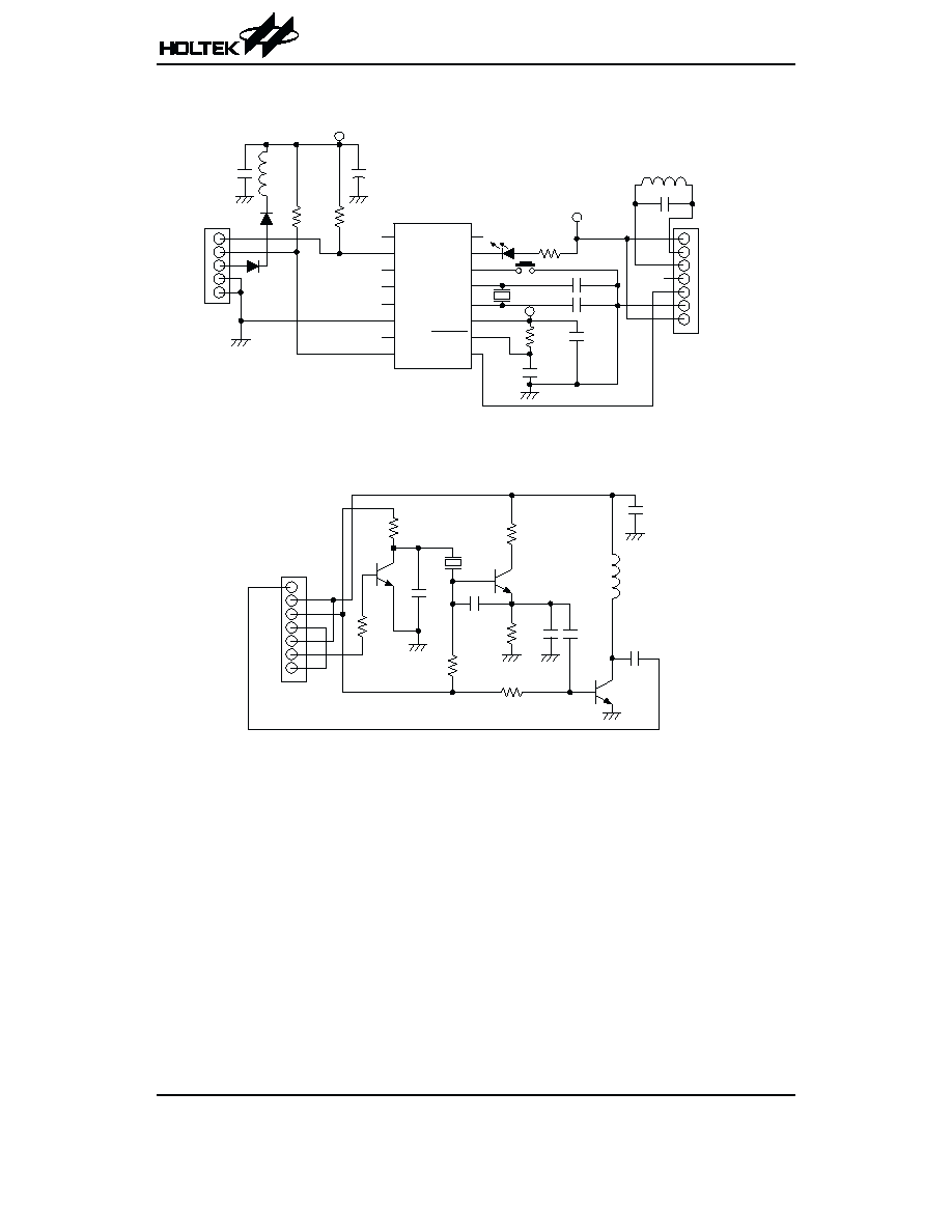
Receiver application (This application circuit is for reference only)
RF transmitter modules
HT82M938T/HT82M938R
Rev. 1.30
6
October 29, 2002
N C
D A T A
N C
N C
N C
V S S
N C
C L K
N C
L E D
R E C _ C H
O S C 2
O S C 1
V D D
R E S E T
R . - I N
H T 8 2 M 9 3 8 R
1
2
3
4
5
6
7
8
1 6
1 5
1 4
1 3
1 2
1 1
1 0
9
6 M H z
V
C C
1 0 0 k W
0 . 1 m .
0 . 1 m .
3 3 p .
3 3 p .
A N T
G N D
V C C
D A T A
1
2
3
4
5
6
7
V
C C
4 7 0 W
E N A B L E
G N D
N C
T A C T / S W 1
1
2
3
4
5
V
C C
3 . 3 k W
3 . 3 k W
1 m H
0 . 1 m .
I N 4 1 4 8
4 7 m . / 6 . 3 V
I N 4 1 4 8
A N T
C P
V C C
A N T
G N D
D A T A
1
2
3
4
5
6
7
G N D
P / E
V C C
1 0 0 k W
2 S C 3 3 5 6
2 0 p .
1 0 k W
2 7 . 1 9 5 M H z
3 3 p .
1 0 0 k W
4 7 k W
4 7 0 W
1 0 0 p .
7 5 p .
0 . 0 0 1 m .
2 . 2 m H
0 . 1 m .
4 7 0 W
2 S C 3 3 5 6
2 S C 3 3 5 6
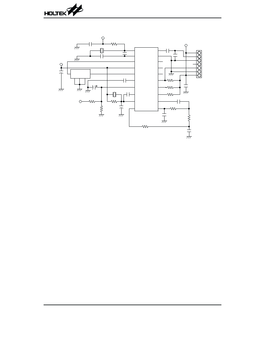
RF receiver modules
Note: For HT9011: place *, **open
For HT9142: place**, *open
HT82M938T/HT82M938R
Rev. 1.30
7
October 29, 2002
H T 9 0 1 1 / H T 9 1 4 2
2 0
1 9
1 8
1 7
1 6
1 5
1 4
1 3
1 2
1 1
1
2
3
4
5
6
7
8
9
1 0
6 8 k W
6 8 k W
M I X I
G N D
R E G O
R E G C
A L M
. S K O
C H G
B S
L P . O
L P . I
O S C I
O S C O
M I X O
V C C
I . I N
D E C
. S K R
I . O
Q U A D
A . O
3 . 3 k W
2 2 p .
3 3 p .
1 0 0 k W
4 7 0 p .
6 8 k W
1 8 0 p .
1 0 0 k W
1 0 0 k W
E N A B L E
A N T
G N D
N C
D A T A
G N D
V C C
0 . 0 1 m .
2 7 M R X / M
V
C C
8 2 p .
1
2
3
4
5
6
7
4 7 p .
4 5 5 k H z / C 2 8
4 5 5 E
3 6 0 k W
1
2
3
4
5
V
C C
1 m . / 1 6 V
0 . 1 m .
1 m .
V
C C
1 5 p .
1 5 p .
2 7 . 6 5 M H z
0 . 0 1 m .
2 2 k W
V
C C
9 1 k W
*
* *
2 2 p .
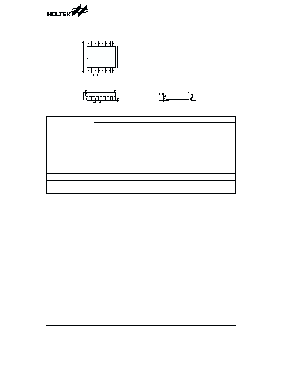
Package Information
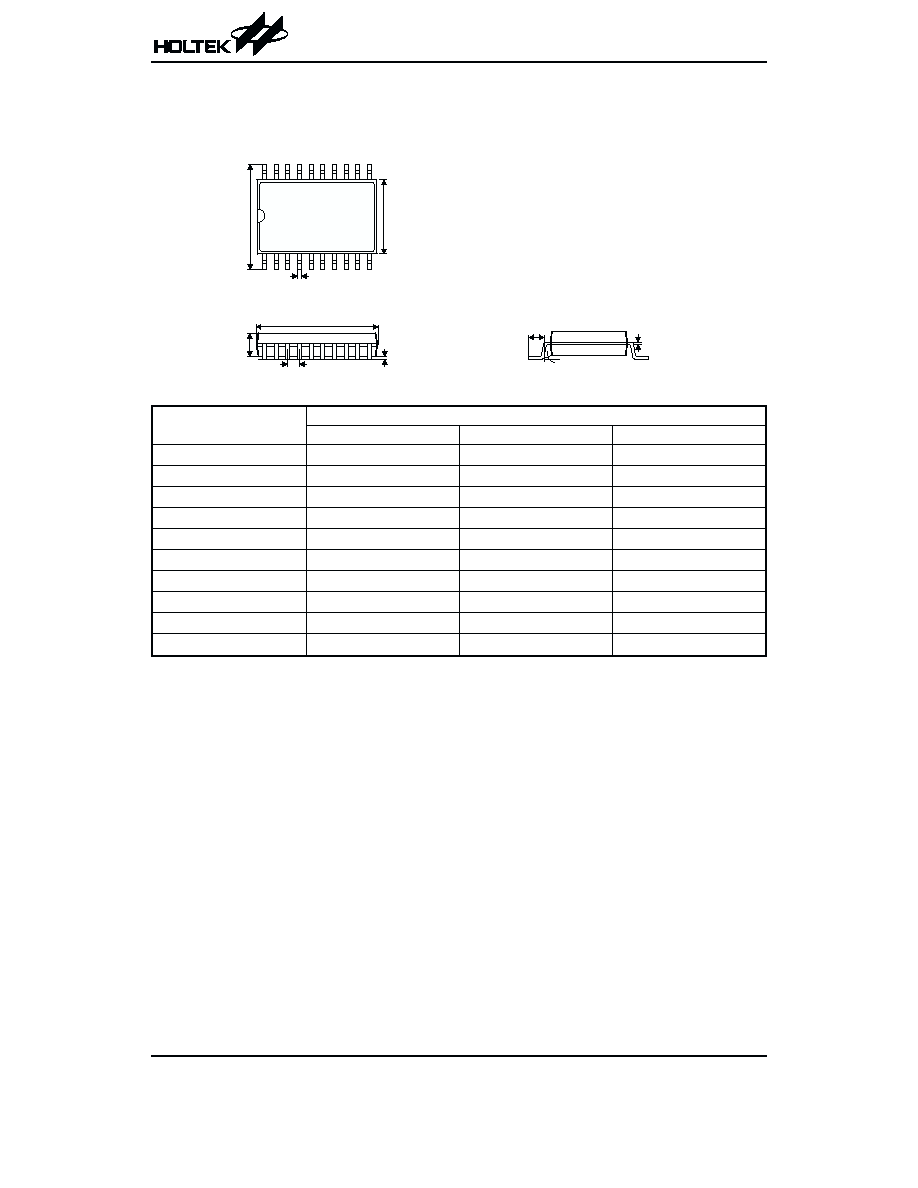
20-pin SOP (300mil) outline dimensions
Symbol
Dimensions in mil
Min.
Nom.
Max.
A
394
¾
419
B
290
¾
300
C
14
¾
20
C
¢
490
¾
510
D
92
¾
104
E
¾
50
¾
F
4
¾
¾
G
32
¾
38
H
4
¾
12
a
0
°
¾
10
°
HT82M938T/HT82M938R
Rev. 1.30
8
October 29, 2002
2 0
1
1 1
1 0
A
B
C
D
E
.
C '
G
H
a
16-pin SOP (300mil) outline dimensions
Symbol
Dimensions in mil
Min.
Nom.
Max.
A
394
¾
419
B
290
¾
300
C
14
¾
20
C
¢
390
¾
413
D
92
¾
104
E
¾
50
¾
F
4
¾
¾
G
32
¾
38
H
4
¾
12
a
0
°
¾
10
°
HT82M938T/HT82M938R
Rev. 1.30
9
October 29, 2002
1 6
1
9
8
a
A
B
C
D
E
.
G
H
C '
Product Tape and Reel Specifications
Reel dimensions
SOP 20W
Symbol
Description
Dimensions in mm
A
Reel Outer Diameter
330
±1.0
B
Reel Inner Diameter
62
±1.5
C
Spindle Hole Diameter
13.0+0.5
-0.2
D
Key Slit Width
2.0
±0.5
T1
Space Between Flange
24.8+0.3
-0.2
T2
Reel Thickness
30.2
±0.2
SOP 16W (300mil)
Symbol
Description
Dimensions in mm
A
Reel Outer Diameter
330
±1.0
B
Reel Inner Diameter
62
±1.5
C
Spindle Hole Diameter
13.0
±0.5
-0.2
D
Key Slit Width
2.0
±0.5
T1
Space Between Flange
16.8+0.3
-0.2
T2
Reel Thickness
22.2
±0.2
HT82M938T/HT82M938R
Rev. 1.30
10
October 29, 2002
A
C
B
T 1
T 2
D
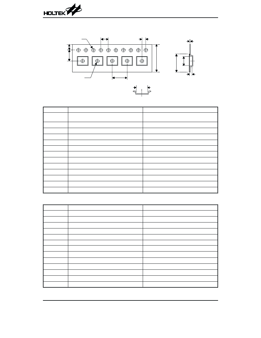
Carrier tape dimensions
SOP 20W
Symbol
Description
Dimensions in mm
W
Carrier Tape Width
24.0+0.3
-0.1
P
Cavity Pitch
12.0
±0.1
E
Perforation Position
1.75
±0.1
F
Cavity to Perforation (Width Direction)
11.5
±0.1
D
Perforation Diameter
1.5+0.1
D1
Cavity Hole Diameter
1.5+0.25
P0
Perforation Pitch
4.0
±0.1
P1
Cavity to Perforation (Length Direction)
2.0
±0.1
A0
Cavity Length
10.8
±0.1
B0
Cavity Width
13.3
±0.1
K0
Cavity Depth
3.2
±0.1
t
Carrier Tape Thickness
0.3
±0.05
C
Cover Tape Width
21.3
SOP 16W (300mil)
Symbol
Description
Dimensions in mm
W
Carrier Tape Width
16.0
±0.2
P
Cavity Pitch
12.0
±0.1
E
Perforation Position
1.75
±0.1
F
Cavity to Perforation (Width Direction)
7.5
±0.1
D
Perforation Diameter
1.5+0.1
D1
Cavity Hole Diameter
1.5+0.25
P0
Perforation Pitch
4.0
±0.1
P1
Cavity to Perforation (Length Direction)
2.0
±0.1
A0
Cavity Length
10.9
±0.1
B0
Cavity Width
10.8
±0.1
K0
Cavity Depth
3.0
±0.1
t
Carrier Tape Thickness
0.3
±0.05
C
Cover Tape Width
13.3
HT82M938T/HT82M938R
Rev. 1.30
11
October 29, 2002
P
D 1
W
P 1
P 0
D
E
.
t
K 0
B 0
A 0
C

HT82M938T/HT82M938R
Rev. 1.30
12
October 29, 2002
Copyright
Ó 200
2
by HOLTEK SEMICONDUCTOR INC.
The information appearing in this Data Sheet is believed to be accurate at the time of publication. However, Holtek as-
sumes no responsibility arising from the use of the specifications described. The applications mentioned herein are used
solely for the purpose of illustration and Holtek makes no warranty or representation that such applications will be suitable
without further modification, nor recommends the use of its products for application that may present a risk to human life
due to malfunction or otherwise. Holtek
¢s products are not authorized for use as critical components in life support devices
or systems. Holtek reserves the right to alter its products without prior notification. For the most up-to-date information,
please visit our web site at http://www.holtek.com.tw.
Holtek Semiconductor Inc. (Headquarters)
No.3, Creation Rd. II, Science Park, Hsinchu, Taiwan
Tel: 886-3-563-1999
Fax: 886-3-563-1189
http://www.holtek.com.tw
Holtek Semiconductor Inc. (Taipei Sales Office)
4F-2, No. 3-2, YuanQu St., Nankang Software Park, Taipei 115, Taiwan
Tel: 886-2-2655-7070
Fax: 886-2-2655-7373
Fax: 886-2-2655-7383 (International sales hotline)
Holtek Semiconductor Inc. (Shanghai Sales Office)
7th Floor, Building 2, No.889, Yi Shan Rd., Shanghai, China 200233
Tel: 021-6485-5560
Fax: 021-6485-0313
http://www.holtek.com.cn
Holtek Semiconductor Inc. (Shenzhen Sales Office)
43F, SEG Plaza, Shen Nan Zhong Road, Shenzhen, China 518031
Tel: 0755-8346
-
5589
Fax: 0755-8346
-
5590
ISDN: 0755-8346
-
5591
Holtek Semiconductor Inc. (Beijing Sales Office)
Suite 1721, Jinyu Tower, A129 West Xuan Wu Men Street, Xicheng District, Beijing, China 100031
Tel: 010-6641
-
0030, 6641
-
7751, 6641
-
7752
Fax: 010-6641
-
0125
Holmate Semiconductor, Inc. (North America Sales Office)
46712 Fremont Blvd., Fremont, CA 94538
Tel: 510-252-9880
Fax: 510-252-9885
http://www.holmate.com
Document Outline
- þÿ
- þÿ
- þÿ
- þÿ
- þÿ
- þÿ
- þÿ
- þÿ
- þÿ
- þÿ