 | –≠–ª–µ–∫—Ç—Ä–æ–Ω–Ω—ã–π –∫–æ–º–ø–æ–Ω–µ–Ω—Ç: HT82K68E | –°–∫–∞—á–∞—Ç—å:  PDF PDF  ZIP ZIP |
Document Outline
- ˛ˇ
- ˛ˇ
- ˛ˇ
- ˛ˇ
- ˛ˇ
- ˛ˇ
- ˛ˇ
- ˛ˇ
- ˛ˇ
- ˛ˇ
- ˛ˇ
- ˛ˇ

HT82K68E
Multimedia Keyboard Encoder OTP
1
August 8, 2000
Features
∑
Operating voltage: 2.8V~5.5V
∑
34(42-pin)/32(40-pin) bidirectional I/O lines
∑
One 8-bit programmable timer counter with
overflow interrupts
∑
Crystal or RC oscillator
∑
Watchdog Timer
∑
3K¥16 OTP EPROM
∑
160¥8 data RAM
∑
HALT function and wake-up feature reduce
power consumption
∑
Six-level subroutine nesting
∑
Bit manipulation instructions
∑
16-bit table read instructions
∑
63 powerful instructions
∑
All instructions in 1 or 2 machine cycles
∑
40/42-pin DIP package
General Description
The HT82K68E is an 8-bit high performance
peripheral interface IC, designed for multiple
I/O products and multimedia applications. It
supports interface to a low speed PC with
multimedia keyboard or wireless keyboard in
Windows 95, Windows 98 or Windows 2000 en-
vironment. A HALT feature is included to re-
duce power consumption.
The program and option PROM can be electri-
cally programmed making the HT82K68E suit-
able for use in product development.
Preliminary

Block Diagram
HT82K68E
2
August 8, 2000
Preliminary
P r o g r a m
C o u n t e r
P r o g r a m
E P R O M
I n s t r u c t i o n
R e g i s t e r
I n s t r u c t i o n
D e c o d e r
T i m i n g
G e n e r a t o r
O S C 2
O S C 1
R E S E T
V D D
V S S
I n t e r r u p t
C i r c u i t
I N T C
M P 0
M P 1
M
U
X
M U X
D A T A
M e m o r y
A L U
S h i f t e r
S T A T U S
A C C
P C C
P C
P O R T C
P C 0 ~ P C 7
T M R
T M R C
S Y S C L K / 4
M
U
X
S Y S C L K / 4
W D T S
W D T P r e s c a l e r
W D T
R C O S C
8 b i t
P D C
P D
P O R T D
P D 0 ~ P D 7
P A C
P A
P O R T A
P A 0 ~ P A 7
P B C
P B
P O R T B
P B 0 ~ P B 7
S T A C K 2
S T A C K 3
S T A C K 0
S T A C K 1
S T A C K 4
S T A C K 5
P E C
P E
P E 0 ~ P E 4
P O R T E

Pin Assignment
Pin Description
Pin Name I/O ROM Code
Option
Description
PA0~PA7
I/O
Wake-up
Pull-high
or None
Bidirectional 8-bit input/output port. Each bit can be configured
as a wake-up input by ROM code option. Software* instructions
determine the CMOS output or schmitt trigger input with or with-
out pull-high resistor 12K.
PB0~PB7
I/O
Pull-high
or None
Bidirectional 8-bit input/output port. Software* instructions de-
termine the CMOS output or schmitt trigger input with or without
pull-high resistor.
PC0
I/O
Wake-up
Pull-high
or None
This pin is an I/O port. Open drain output with pull-high resistor
and can be used as DATA or CLOCK line of PS2. This pin can be
configured as a wake-up input by ROM code option.
PC1
I/O
Wake-up
Pull-high
or None
This pin is an I/O port. open drain output with pull-high resistor
and can be used as DATA or CLOCK line of . This pin can be con-
figured as a wake-up input by ROM code option.
HT82K68E
3
August 8, 2000
Preliminary
P B 6
P B 7
P A 4
P A 5
P A 6
P A 7
O S C 2
O S C 1
V D D
R E S E T
P E 4 ( L E D )
P D 3
P D 2
P D 1
P D 0
P C 7
P C 6
P C 5
P C 4
P C 3
P B 5
P B 4
P A 3
P A 2
P A 1
P A 0
P B 3
P B 2
P B 1
P B 0
P D 7
P D 6
P D 5
P D 4
V S S
P E 2 ( L E D )
P E 3 ( L E D )
P C 0
P C 1
P C 2
4 0
3 9
3 8
3 7
3 6
3 5
3 4
3 3
3 2
3 1
3 0
2 9
2 8
2 7
2 6
2 5
2 4
2 3
2 2
2 1
1
2
3
4
5
6
7
8
9
1 0
1 1
1 2
1 3
1 4
1 5
1 6
1 7
1 8
1 9
2 0
4 2
4 1
4 0
3 9
3 8
3 7
3 6
3 5
3 4
3 3
3 2
3 1
3 0
2 9
2 8
2 7
2 6
2 5
2 4
2 3
2 2
1
2
3
4
5
6
7
8
9
1 0
1 1
1 2
1 3
1 4
1 5
1 6
1 7
1 8
1 9
2 0
2 1
P B 5
P B 4
P A 3
P A 2
P A 1
P A 0
P B 3
P B 2
P B 1
P B 0
P D 7
P D 6
P D 5
P D 4
V S S
P E 2 ( L E D )
P E 3 ( L E D )
P C 0
P C 1
P C 2
P E 0
P B 6
P B 7
P A 4
P A 5
P A 6
P A 7
O S C 2
O S C 1
V D D
R E S E T
P E 4 ( L E D )
P D 3
P D 2
P D 1
P D 0
P C 7
P C 6
P C 5
P C 4
P C 3
P E 1
H T 8 2 K 6 8 E
4 0 D I P
H T 8 2 K 6 8 E
4 2 D I P

Pin Name I/O ROM Code
Option
Description
PC2~PC3
I/O
Wake-up
Pull-high
or None
Bidirectional 2-bit input/output port. Each bit can be configured
as a wake-up input by ROM code option. Software* instructions
determine the CMOS output or schmitt trigger input with or with-
out pull-high resistor.
PC4~PC7
I/O
Pull-high
or None
Bidirectional 4-bit input/output port. Software* instructions de-
termine the CMOS output or schmitt trigger input with or without
pull-high resistor.
PD0~PD7
I/O
Pull-high
or None
Bidirectional 8-bit input/output port. Software* instructions de-
termine the CMOS output or schmitt trigger input with or without
pull-high resistor.
PE0~PE1
I/O
Pull-high
or None
Bidirectional input/output port. Software* instructions determine
the CMOS output or schmitt trigger input with or without
pull-high resistor.
PE2~PE4
O
æ
This pin is an NMOS output structure. The pad can function as
LED drivers for the keyboard. I
OL
=14mA, @V
OL
=3.2V
VDD
æ
æ
Positive power supply
VSS
æ
æ
Negative power supply, ground
RESET
I
æ
Chip reset input. Active low. Built-in power-on reset circuit to re-
set the entire chip. Chip can also be externally reset via RESET
pin
OSC1
OSC2
I
O
Crystal or
RC
OSC1, OSC2 are connected to an RC network or a crystal for the
internal system clock. In the case of RC operation, OSC2 is the
output terminal for the 1/4 system clock; A 110kW resistor is con-
nected to OSC1 to generate a 2MHZ frequency.
Note: *: Software means the ROM code option can be configured by HT-IDE (Holtek Integrated De-
velopment Environment).
Absolute Maximum Ratings
Supply Voltage .............................-0.3V to 5.5V
Storage Temperature ................-50∞C to 125∞C
Input Voltage ................V
SS
-0
.
3V to V
DD
+0.3V
Operating Temperature .............-25∞C to 70∞C
Note: These are stress ratings only. Stresses exceeding the range specified under ≤Absolute Maxi-
mum Ratings≤ may cause substantial damage to the device. Functional operation of this device
at other conditions beyond those listed in the specification is not implied and prolonged expo-
sure to extreme conditions may affect device reliability.
HT82K68E
4
August 8, 2000
Preliminary

D.C. Characteristics
Ta=25∞C
Symbol
Parameter
Test Conditions
Min. Typ. Max. Unit
V
DD
Conditions
V
DD
Operating Voltage
æ
æ
2.8
æ
5.5
V
I
DD1
Operating Current
(Crystal OSC)
3V
No load, f
SYS
= 2MHz
æ
0.7
1.5
mA
5V
æ
2
5
mA
I
DD2
Operating Current
(RC OSC)
3V
No load, f
SYS
= 2MHz
æ
1
1.5
mA
5V
æ
2
5
mA
I
STB1
Standby Current
(WDT enabled)
3V
No load, system HALT
æ
æ
8
mA
5V
æ
æ
15
mA
I
STB2
Standby Current
(WDT Disabled)
3V
No load, system HALT
æ
æ
3
mA
5V
æ
æ
6
mA
V
IL
Input Low Voltage for
I/O Ports
3V
æ
0
æ
1
V
5V
æ
0
æ
1.5
V
V
IH
Input High Voltage for
I/O Ports
3V
æ
2.1
æ
3
V
5V
æ
3.5
æ
5
V
V
IL1
Input Low Voltage
(RESET)
3V
æ
0
æ
0.7
V
5V
æ
0
æ
1.3
V
V
IH1
Input High Voltage
(RESET)
3V
æ
2.5
æ
3
V
5V
æ
4.1
æ
5
V
I
OL
I/O Port Sink Current
5V V
OL
= 0.5V
7
15
æ
mA
I
OH
I/O Port Source Current
5V V
OH
= 4.5V
-2.5 -4.5
æ
mA
I
LED
LED Sink Current
5V V
OL
=3.2V
10
14
18
mA
t
POR
Power-on Reset Time
5V
æ
120
150
180
ms
R
PH
Internal Pull-high
Resistance of PA, PB, PC,
PD, PE Port
5V
æ
5
12
20
kW
R
PH1
Internal Pull-high
Resistance of DATA, CLK 5V
æ
2
5
8
kW
Df/f
Frequency Variation
5V Crystal
æ
æ
±1
%
Df/f1
Frequency Variation
5V RC
æ
æ
±10
%
HT82K68E
5
August 8, 2000
Preliminary

A.C. Characteristics
Ta=25∞C
Symbol
Parameter
Test Conditions
Min. Typ. Max. Unit
V
DD
Conditions
f
SYS1
System Clock
(Crystal OSC)
3V
æ
æ
2
æ
MHz
5V
æ
æ
2
20
MHz
f
SYS2
System Clock (RC OSC)
3V
æ
æ
2
æ
MHz
5V
æ
æ
2
20
MHz
t
WDTOSC
Watchdog Oscillator
3V
æ
45
90
180
ms
5V
æ
35
65
130
ms
t
WDT1
Watchdog Time-out
Period (RC)
3V
Without WDT
prescaler
12
23
45
ms
5V
9
17
35
ms
t
WDT2
Watchdog Time-out
Period (System Clock)
æ
Without WDT
prescaler
æ
1024
æ
t
SYS
t
RES
External Reset Low
Pulse Width
æ
æ
1
æ
æ
ms
t
SST
System Start-up Timer
Period
æ
Power-up or
wake-up from HALT æ
1024
æ
t
SYS
t
INT
Interrupt Pulse Width
æ
æ
1
æ
æ
ms
Note: t
SYS
= 1/f
SYS
HT82K68E
6
August 8, 2000
Preliminary

HT82K68E
7
August 8, 2000
Preliminary
T 1
T 2
T 3
T 4
T 1
T 2
T 3
T 4
T 1
T 2
T 3
T 4
F e t c h I N S T ( P C )
E x e c u t e I N S T ( P C - 1 )
F e t c h I N S T ( P C + 1 )
E x e c u t e I N S T ( P C )
F e t c h I N S T ( P C + 2 )
E x e c u t e I N S T ( P C + 1 )
P C
P C + 1
P C + 2
S y s t e m C l o c k
O S C 2 ( R C o n l y )
P C
( N M O S o p e n d r a i n o u t p u t )
Execution flow
Functional Description
Execution flow
The HT82K68E system clock is derived from ei-
ther a crystal or an RC oscillator. The system
clock is internally divided into four
non-overlapping clocks. One instruction cycle
consists of four system clock cycles.
Instruction fetching and execution are
pipelined in such a way that a fetch takes one
instruction cycle while decoding and execution
takes the next instruction cycle. However, the
pipelining scheme causes each instruction to
effectively execute within one cycle. If an in-
struction changes the program counter, two cy-
cles are required to complete the instruction.
Program counter - PC
The 12-bit program counter (PC) controls the
sequence in which the instructions stored in the
program ROM are executed and its contents
specify a maximum of 4096 addresses.
After accessing a program memory word to
fetch an instruction code, the contents of the
program counter are incremented by one. The
program counter then points to the memory
word containing the next instruction code.
When executing a jump instruction, conditional
skip execution, loading PCL register, subrou-
tine call, initial reset, internal interrupt, exter-
nal interrupt or return from subroutine, the PC
manipulates the program transfer by loading
the address corresponding to each instruction.
The conditional skip is activated by instruction.
Once the condition is met, the next instruction,
fetched during the current instruction execu-
tion, is discarded and a dummy cycle replaces it
to get the proper instruction. Otherwise pro-
ceed with the next instruction.
The lower byte of the program counter (PCL) is
a readable and writeable register (06H). Moving
data into the PCL performs a short jump. The
destination will be within 256 locations.
Once a control transfer takes place, an addi-
tional dummy cycle is required.
Program memory - PROM
The program memory is used to store the pro-
gram instructions which are to be executed. It
also contains data, table, and interrupt entries,
and is organized with 3072 ¥ 16 bits, addressed
by the program counter and table pointer.
Certain locations in the program memory are
reserved for special usage:
∑
Location 000
This area is reserved for the initialization
program. After chip reset, the program al-
ways begins execution at location 000H.

Mode
Program Counter
*11 *10 *9
*8
*7
*6
*5
*4
*3
*2
*1
*0
Initial reset
0
0
0
0
0
0
0
0
0
0
0
0
Timer counter overflow
0
0
0
0
0
0
0
0
1
0
0
0
Skip
PC+2
Loading PCL
*11 *10 *9
*8 @7 @6 @5 @4 @3 @2 @1 @0
Jump, call branch
#11 #10 #9
#8
#7
#6
#5
#4
#3
#2
#1
#0
Return from subroutine
S11 S10 S9 S8 S7 S6 S5 S4 S3 S2 S1 S0
HT82K68E
8
August 8, 2000
Preliminary
Note: *11~*0: Program counter bits
#11~#0: Instruction code bits
S11~S0: Stack register bits
@7~@0: PCL bits
∑
Location 008H
This area is reserved for the timer counter in-
terrupt service program. If timer interrupt re-
sults from a timer counter overflow, and if the
interrupt is enabled and the stack is not full,
the program begins execution at location
008H.
∑
Table location
Any location in the PROM space can be used
as look-up tables. The instructions TABRDC
[m] (the current page, 1 page=256 words) and
TABRDL [m] (the last page) transfer the con-
tents of the lower-order byte to the specified
data memory, and the higher-order byte to
TBLH (08H). Only the destination of the
lower-order byte in the table is well-defined,
the other bits of the table word are trans-
ferred to the lower portion of TBLH, the re-
maining 1 bit is read as 0. The Table
Higher-order byte register (TBLH) is read
only. The TBLH is read only and cannot be re-
stored. If the main routine and the ISR (Inter-
rupt Service Routine) both employ the table
read instruction, the contents of the TBLH in
the main routine are likely to be changed by
the table read instruction used in the ISR. Er-
rors can occur. In other words, using the table
read instruction in the main routine and the
ISR simultaneously should be avoided. How-
ever, if the table read instruction has to be ap-
plied in both the main routine and the ISR,
the interrupt is supposed to be disabled prior
to the table read instruction. It will not be en-
abled until the TBLH has been backed up.
The table pointer (TBLP) is a read/write regis-
ter (07H), which indicates the table location.
Before accessing the table, the location must be
placed in TBLP. All table related instructions
need 2 cycles to complete the operation. These
areas may function as normal program memory
depending upon the requirements.
0 0 0 H
0 0 8 H
D e v i c e i n i t i a l i z a t i o n p r o g r a m
T i m e r / e v e n t c o u n t e r i n t e r r u p t s u b r o u t i n e
P r o g r a m
P R O M
1 6 b i t s
L o o k - u p t a b l e ( 2 5 6 w o r d s )
n 0 0 H
L o o k - u p t a b l e ( 2 5 6 w o r d s )
B F F H
N o t e : n r a n g e s f r o m 0 t o B
n F F H
Program memory

Instruction(s)
Table Location
*11
*10
*9
*8
*7
*6
*5
*4
*3
*2
*1
*0
TABRDC [m]
P11 P10
P9
P8
@7
@6
@5
@4
@3
@2
@1
@0
TABRDL [m]
1
0
1
1
@7
@6
@5
@4
@3
@2
@1
@0
HT82K68E
9
August 8, 2000
Preliminary
Note: *11~*0: Table location bits
@7~@0: Table location bits
P11~P8: Current program counter bits
Stack register - STACK
This is a special part of the memory which is
used to save the contents of the program coun-
ter (PC) only. The stack is organized into six lev-
els and is neither part of the data nor part of the
program space, and is neither readable nor
writeable. The activated level is indexed by the
stack pointer (SP) and is neither readable nor
writeable. At a subroutine call or interrupt ac-
knowledgement, the contents of the program
counter are pushed onto the stack. At the end of
a subroutine or an interrupt routine, signaled
by a return instruction (RET or RETI), the pro-
gram counter is restored to its previous value
from the stack. After a chip reset, the SP will
point to the top of the stack.
If the stack is full and a non-masked interrupt
takes place, the interrupt request flag will be re-
corded but the acknowledgement will be inhib-
ited. When the stack pointer is decremented (by
RET or RETI), the interrupt will be serviced. This
feature prevents stack overflow allowing the pro-
grammer to use the structure more easily. In a
similar case, if the stack is full and a ≤CALL≤ is
subsequently executed, stack overflow occurs and
the first entry will be lost (only the most recent
four return addresses are stored).
Data memory - RAM
The data memory is designed with 184 ¥ 8 bits.
It is divided into two functional groups: special
function registers and general purpose data
memory (160¥8). Most of them are read/write,
but some are read only.
The special function registers include the Indi-
rect Addressing register 0 (00H), the Memory
Pointer register 0 (MP0;01H), the Indirect Ad-
dressing register 1 (02H), the Memory Pointer
register 1 (MP1;03H), the Accumulator
(ACC;05H), the Program Counter Lower-byte
register (PCL;06H), the Table Pointer
(TBLP;07H), the Table Higher-order byte regis-
ter (TBLH;08H), the Watchdog Timer option Set-
ting register (WDTS;09H), the Status register
I n d i r e c t A d d r e s s i n g R e g i s t e r 0
M P 0
I n d i r e c t A d d r e s s i n g R e g i s t e r 1
M P 1
A C C
P C L
T B L P
T B L H
W D T S
S T A T U S
I N T C
T M R
T M R C
P A
P A C
P B
P B C
P C
P C C
P D
P D C
P E
P E C
G e n e r a l P u r p o s e
D A T A M E M O R Y
( 1 6 0 B y t e s )
S p e c i a l P u r p o s e
D A T A M E M O R Y
0 0 H
0 1 H
0 2 H
0 3 H
0 4 H
0 5 H
0 6 H
0 7 H
0 8 H
0 9 H
0 A H
0 B H
0 C H
0 D H
0 E H
0 F H
1 0 H
1 1 H
1 2 H
1 3 H
1 4 H
1 5 H
1 6 H
1 7 H
1 8 H
1 9 H
1 A H
1 B H
1 C H
1 D H
1 E H
1 F H
F F H
: U n u s e d .
R e a d a s ≤ 0 0 ≤
2 0 H
6 0 H
RAM mapping

HT82K68E
10
August 8, 2000
Preliminary
(STATUS;0AH), the Interrupt Control register
(INTC;0BH), the timer counter register
(TMR;0DH), the timer counter control register
(TMRC;0EH), the I/O registers (PA;12H,
PB;14H, PC;16H, PD;18H, PE;1AH) and the I/O
control registers (PAC;13H, PBC;15H, PCC;17H,
PDC;19H, PEC;1BH). The remaining space be-
fore the 60H is reserved for future expanded us-
age and reading these locations will get the result
00H. The general purpose data memory, ad-
dressed from 60H to FFH, is used for data and
control information under instruction com-
mand.
All data memory areas can handle arithmetic,
logic, increment, decrement and rotate opera-
tions directly. Except for some dedicated bits,
each bit in the data memory can be set and re-
set by the SET [m].i and CLR [m].i instructions,
respectively. They are also indirectly accessible
through Memory pointer registers (MP0;01H,
MP1;03H).
Indirect addressing register
Location 00H and 02H are indirect addressing
registers that are not physically implemented.
Any read/write operation of [00H] and [02H]
can access the data memory pointed to by MP0
(01H) and MP1 (03H) respectively. Reading lo-
cation 00H or 02H indirectly will return the re-
sult 00H. Writing indirectly results in no
operation.
The function of data movement between two in-
direct addressing registers is not supported.
The memory pointer registers, MP0 and MP1,
are 8-bit registers which can be used to access
the data memory by combining corresponding
indirect addressing registers.
Accumulator
The accumulator is closely related to the ALU
operations. It is also mapped to location 05H of
the data memory and is capable of carrying out
immediate data operations. The data move-
ment between two data memory locations must
pass through the accumulator.
Arithmetic and logic unit - ALU
This circuit performs 8-bit arithmetic and logic
operation. The ALU provides the following func-
tions:
∑
Arithmetic operations (ADD, ADC, SUB,
SBC, DAA)
∑
Logic operations (AND, OR, XOR, CPL)
∑
Rotation (RL, RR, RLC, RRC)
∑
Increment and Decrement (INC, DEC)
∑
Branch decision (SZ, SNZ, SIZ, SDZ ....)
The ALU not only saves the results of a data op-
eration but also changes the status register.
Status register - Status
The 8-bit status register (0AH) contains the
zero flag (Z), carry flag (C), auxiliary carry flag
(AC), overflow flag (OV), power down flag (PD)
and watch dog time-out flag (TO). The status
register not only records the status information
but also controls the operation sequence.
With the exception of the TO and PD flags, bits
in the status register can be altered by instruc-
tions like most other registers. Any data writ-
ten into the status register will not change the
TO or PD flags. It should be noted that opera-
tions related to the status register may give dif-
ferent results from those intended. The TO and
PD flags can only be changed by system power
up, Watchdog Timer overflow, executing the
HALT instruction and clearing the Watchdog
Timer.
The Z, OV, AC and C flags generally reflect the
status of the latest operations.
In addition, on entering an interrupt sequence
or executing a subroutine call, the status regis-
ter will not be automatically pushed onto the
stack. If the contents of status are important
and if the subroutine can corrupt the status
register, precaution must be taken to save it
properly.

HT82K68E
11
August 8, 2000
Preliminary
Labels
Bits
Function
C
0
C is set if the operation results in a carry during an addition operation or if a bor-
row does not take place during a subtraction operation; otherwise C is cleared. C
is also affected by a rotate through carry instruction.
AC
1
AC is set if the operation results in a carry out of the low nibbles in addition or if
no borrow from the high nibble into the low nibble in subtraction; otherwise AC
is cleared.
Z
2
Z is set if the result of an arithmetic or logic operation is zero; otherwise Z is
cleared.
OV
3
OV is set if the operation results in a carry into the highest-order bit but not a
carry out of the highest-order bit, or vice versa; otherwise OV is cleared.
PD
4
PD is cleared when either a system power-up or executing the CLR WDT in-
struction. PD is set by executing the HALT instruction.
TO
5
TO is cleared by a system power-up or executing the CLR WDT or HALT in-
struction. TO is set by a WDT time-out.
æ
6
Undefined, read as "0"
æ
7
Undefined, read as "0"
Status register
Interrupt
The HT82K68E provides an internal timer
counter interrupt. The interrupt control regis-
ter (INTC;0BH) contains the interrupt control
bits to set not only the enable/disable status but
also the interrupt request flags.
Once an interrupt subroutine is serviced, all
other interrupts will be blocked (by clearing the
EMI bit). This scheme may prevent any further
interrupt nesting. Other interrupt requests may
occur during this interval but only the interrupt
request flag is recorded. If a certain interrupt re-
quires servicing within the service routine, the
EMI bit and the corresponding bit of the INTC
may be set to allow interrupt nesting. If the
stack is full, the interrupt request will not be ac-
knowledged, even if the related interrupt is en-
abled, until the SP is decremented. If immediate
service is desired, the stack must be prevented
from becoming full.
All these kinds of interrupt have the wake-up
capability. As an interrupt is serviced, a control
transfer occurs by pushing the program counter
onto the stack followed by a branch to a subrou-
tine at the specified location in the program
memory. Only the program counter is pushed
onto the stack. If the contents of the register and
Status register (STATUS) are altered by the in-
terrupt service program which corrupt the de-
sired control sequence, the contents should be
saved in advance.
The internal timer counter interrupt is initialized
by setting the timer counter interrupt request
flag (T0F; bit 5 of INTC), which is normally
caused by a timer counter overflow. When the in-
terrupt is enabled, and the stack is not full and
the T0F bit is set, a subroutine call to location
08H will occur. The related interrupt request flag
(T0F) will be reset and the EMI bit cleared to dis-
able further interrupts.
During the execution of an interrupt subroutine,
other interrupt acknowledgements are held un-
til the RETI instruction is executed or the EMI
bit and the related interrupt control bit are set to
1 (if the stack is not full). To return from the in-
terrupt subroutine, a RET or RETI instruction
may be invoked. RETI will set the EMI bit to en-
able an interrupt service, but RET will not.
Interrupts occurring in the interval between
the rising edges of two consecutive T2 pulses,

HT82K68E
12
August 8, 2000
Preliminary
will be serviced on the latter of the two T2
pulses, if the corresponding interrupts are en-
abled. In the case of simultaneous requests, the
following table shows the priority that is ap-
plied. These can be masked by resetting the
EMI bit.
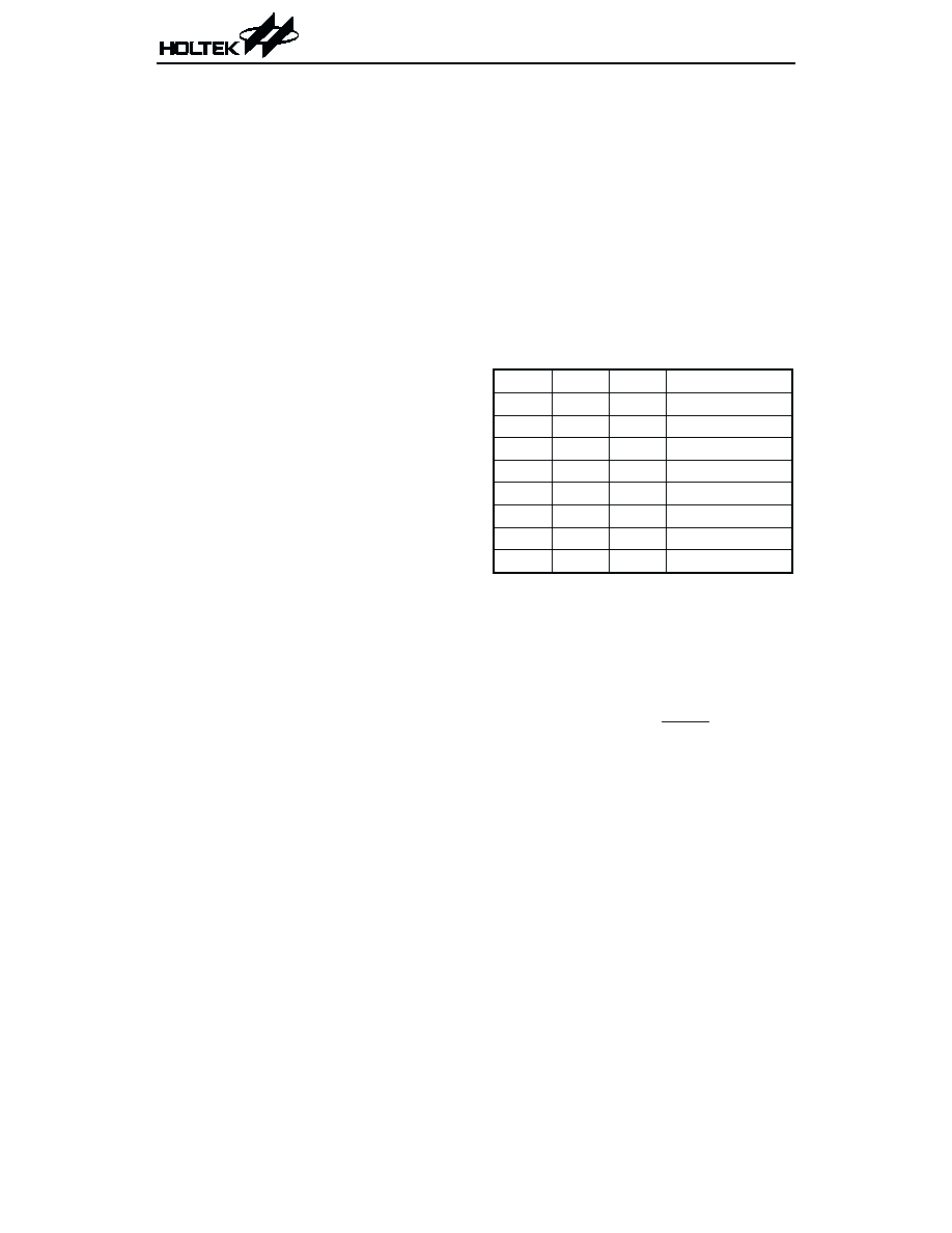
No.
Interrupt Source
Vector
a
Timer counter overflow
08H
The timer counter interrupt request flag (T0F),
enable timer counter bit (ET0I), and enable
master interrupt bit (EMI) constitute an inter-
rupt control register (INTC) which is located at
0BH in the data memory. EMI, ET0I, are used
to control the enabling/disabling of interrupts.
These bits prevent the requested interrupt
from being serviced. Once the interrupt request
flags (T0F) are set, they will remain in the
INTC register until the interrupts are serviced
or cleared by a software instruction.
It is suggested that a program does not use the
≤CALL subroutine≤ within the interrupt sub-
routine. Because interrupts often occur in an un-
predictable manner or need to be serviced
immediately in some applications, if only one
stack is left and enabling the interrupt is not well
controlled, once the ≤CALL subroutine≤ operates in
the interrupt subroutine it will damage the original
control sequence.
Oscillator configuration
There are two oscillator circuits in HT82K68E.
Both are designed for system clocks; the RC os-
cillator and the Crystal oscillator, which are de-
termined by mask options. No matter what
oscillator type is selected, the signal provides
the system clock. The HALT mode stops the
system oscillator and resists the external signal
to conserve power.
Register
Bit No.
Label
Function
INTC
(0BH)
0
EMI
Controls the master (global) interrupt
(1= enabled; 0= disabled)
1
æ
Undefined, read as "0"; programming must be "0"
2
ET0I
Controls the timer counter interrupt
(1= enabled; 0= disabled)
3
æ
Undefined, read as "0"
4
æ
Undefined, read as "0"; programming must be "0"
5
T0F
Internal timer counter request flag
(1= active; 0= inactive)
6
æ
Undefined, read as "0"
7
æ
Unused bit, read as "0"
INTC register
Crystal Oscillator
RC Oscillator
OSC1
OSC2
OSC1
OSC2
V
DD
f
SYS
/4
(NMOS Open
Drain Output)
System oscillator
HT82K68E
13
August 8, 2000
Preliminary
If an RC oscillator is used, an external resistor
between OSC1 and VDD is needed and the re-
sistance must range from 51kW to 1MW. The
system clock, divided by 4, is available on
OSC2, which can be used to synchronize exter-
nal logic. The RC oscillator provides the most
cost effective solution. However, the frequency
of the oscillation may vary with VDD, tempera-
ture and the chip itself due to process varia-
tions. It is, therefore, not suitable for timing
sensitive operations where accurate oscillator
frequency is desired.
If the Crystal oscillator is used, a crystal across
OSC1 and OSC2 is needed to provide the feed-
back and phase shift needed for oscillator, no
other external components are needed. Instead
of a crystal, the resonator can also be connected
between OSC1 and OSC2 to get a frequency ref-
erence, but two external capacitors in OSC1
and OSC2 are required.
The WDT oscillator is a free running on-chip
RC oscillator, and no external components are
required. Even if the system enters the power
down mode, the system clock is stopped, but the
WDT oscillator still works for a period of ap-
proximately 78 ms. The WDT oscillator can be
disabled by mask option to conserve power.
Watchdog Timer - WDT
The WDT clock source is implemented by a ded-
icated RC oscillator (WDT oscillator) or instruc-
tion clock (system clock divided by 4), decided
by mask options. This timer is designed to pre-
vent a software malfunction or sequence jump-
ing to an unknown location with unpredictable
results. The Watchdog Timer can be disabled by
mask option. If the Watchdog Timer is disabled,
all the executions related to the WDT results in
no operation.
Once the internal WDT oscillator (RC oscillator
normally with a period of 78ms) is selected, it is
first divided by 256 (8-stages) to get the nomi-
nal time-out period of approximately 20 ms.
This time-out period may vary with tempera-
ture, VDD and process variations. By invoking
the WDT prescaler, longer time-out periods can
be realized. Writing data to WS2, WS1, WS0
(bit 2,1,0 of the WDTS) can give different
time-out periods. If WS2, WS1, WS0 are all
equal to 1, the division ratio is up to 1:128, and
the maximum time-out period is 2.6 seconds.
If the WDT oscillator is disabled, the WDT clock
may still come from the instruction clock and
operate in the same manner except that in the
HALT state the WDT may stop counting and
lose its protecting purpose. In this situation the
WDT logic can be restarted by external logic.
The high nibble and bit 3 of the WDTS are re-
served for user defined flags, which can be used
to indicate some specified status.
If the device operates in a noisy environment,
using the on-chip RC oscillator (WDT OSC) is
strongly recommended, since the HALT will
stop the system clock.
WS2
WS1
WS0
Division Ratio
0
0
0
1:1
0
0
1
1:2
0
1
0
1:4
0
1
1
1:8
1
0
0
1:16
1
0
1
1:32
1
1
0
1:64
1
1
1
1:128
The WDT overflow under normal operation will
initialize ≤chip reset≤ and set the status bit TO. An
overflow in the HALT mode, initializes a ≤warm
reset≤ only when the PC and SP are reset to zero.
To clear the contents of the WDT (including the
WDT prescaler ), three methods are adopted; ex-
ternal reset (a low level to RESET), software in-
struction(s), or a HALT instruction. There are two
types of software instructions; CLR WDT and
CLR WDT1/CLR WDT2. Of these two types of in-
struction, only one can be active depending on the
mask option - ≤CLR WDT times selection option≤.
If the ≤CLR WDT≤ is selected (ie. CLR WDT times
equal one), any execution of the CLR WDT in-
struction will clear the WDT. In case ≤CLR WDT1≤
and ≤CLR WDT2≤ are chosen (ie. CLRWDT times
equal two), these two instructions must be exe-
WDTS register

HT82K68E
14
August 8, 2000
Preliminary
cuted to clear the WDT; otherwise, the WDT may
reset the chip because of the time-out.
Power down operation - HALT
The HALT mode is initialized by the HALT in-
struction and results in the following...
∑
The system oscillator will turn off but the
WDT oscillator keeps running (if the WDT os-
cillator is selected).
∑
The contents of the on chip RAM and regis-
ters remain unchanged.
∑
WDT and WDT prescaler will be cleared and
recount again (if the WDT clock has come
from the WDT oscillator).
∑
All I/O ports maintain their original status.
∑
The PD flag is set and the TO flag is cleared.
The system can leave the HALT mode by means
of an external reset, an external falling edge
signal on port A and port C [0:3] or a WDT over-
flow. An external reset causes a device initializa-
tion and the WDT overflow performs a ≤warm
reset≤. Examining the TO and PD flags, the rea-
son for chip reset can be determined. The PD flag
is cleared when system power-up or executing the
CLR WDT instruction and is set when the HALT
instruction is executed. The TO flag is set if the
WDT time-out occurs, and causes a wake-up that
only resets the PC and SP, the others keep their
original status.
The port A or port C [0:3] wake-up can be con-
sidered as a continuation of normal execution.
Each bit in port A can be independently se-
lected to wake up the device by mask option.
Awakening from an I/O port stimulus, the pro-
gram will resume execution of the next instruc-
tion.
Once a wake-up event occurs, and the system
clock comes from a crystal, it takes 1024 t
SYS
(system clock period) to resume normal opera-
tion. In other words, the HT82K68E will insert
a dummy period after the wake-up. If the sys-
tem clock comes from an RC oscillator, it contin-
ues operating immediately. If the wake-up
results in next instruction execution, this will
execute immediately after the dummy period is
completed.
To minimize power consumption, all I/O pins
should be carefully managed before entering
the HALT status.
Reset
There are three ways in which a reset can occur:
∑
RESET reset during normal operation
∑
RESET reset during HALT
∑
WDT time-out reset during normal operation
The WDT time-out during HALT is different
from other chip reset conditions, since it can
perform a warm reset that just resets the PC
and SP, leaving the other circuits to remain in
their original state. Some registers remain un-
changed during other reset conditions. Most
registers are reset to the ≤initial condition≤
S y s t e m c l o c k / 4
8 - b i t C o u n t e r
W D T P r e s c a l e r
7 - b i t C o u n t e r
8 - t o - 1 M U X
W D T T i m e - o u t
W S 0 ~ W S 2
R O M
C o d e
O p t i o n
S e l e c t
W D T
O S C
Watchdog Timer
R E S E T
V D D
S S T T i m e - o u t
C h i p R e s e t
t
S S T
Reset timing chart

HT82K68E
15
August 8, 2000
Preliminary
when the reset conditions are met. By examin-
ing the PD and TO flags, the program can dis-
tinguish between different ≤chip resets≤.
TO
PD
RESET Conditions
0
0
RESET reset during power-up
u
u
RESET reset during normal
operation
0
1
RESET wake-up HALT
1
u
WDT time-out during normal
operation
1
1
WDT wake-up HALT
Note: ≤u≤ means ≤unchanged≤
To guarantee that the system oscillator has
started and stabilized, the SST (System
Start-up Timer) provides an extra-delay of 1024
system clock pulses when the system powers up
or when it awakes from the HALT state.
When a system power-up occurs, the SST delay
is added during the reset period. But when the
reset comes from the RESET pin, the SST delay
is disabled. Any wake-up from HALT will en-
able the SST delay.
The functional unit chip reset status is shown
below.
PC
000H
Prescaler
Clear
WDT
Clear. After master re-
set, WDT begins count-
ing
Timer counter
Off
Input/output ports Input mode
SP
Points to the top of
the stack
Timer counter
A timer counter (TMR) is implemented in the
HT82K68E. The timer counter contains an
8-bit programmable count-up counter and the
clock may come from the system clock divided
by 4.
Using the internal instruction clock, there is
only one reference time-base.
There are two registers related to the timer
counter; TMR ([0DH]), TMRC ([0EH]). Two
physical registers are mapped to TMR location;
writing TMR makes the starting value be
placed in the timer counter preload register and
reading TMR gets the contents of the timer
counter. The TMRC is a timer counter control
register, which defines some options.
In the timer mode, once the timer counter
starts counting, it will count from the current
contents in the timer counter to FFH. Once
overflow occurs, the counter is reloaded from
the timer counter preload register and gener-
ates the interrupt request flag (TF; bit 5 of
INTC) at the same time.
R E S E T
V
D D
Reset circuit
W D T
H A L T
W D T
T i m e - o u t
R e s e t
R E S E T
C o l d
R e s e t
P o w e r - o n D e t e c t i o n
S S T
1 0 - s t a g e
R i p p l e C o u n t e r
O S C 1
W a r m R e s e t
Reset configuration

HT82K68E
16
August 8, 2000
Preliminary
Label
Bits
Function
æ
0~3
Unused bits, read as "0"
TON
4
To enable/disable timer counting
(0= disabled; 1= enabled)
æ
5
Unused bits, read as "0"
TM0
TM1
6
7
10= Timer mode (internal clock)
TMRC register
To enable the counting operation, the timer
ON bit (TON; bit 4 of TMRC) should be set to 1.
In the case of timer counter OFF condition,
writing data to the timer counter preload reg-
ister will also reload that data to the timer
counter. But if the timer counter is turned on,
data written to it will only be kept in the
timer counter preload register. The timer coun-
ter will still operate until overflow occurs. When
the timer counter (reading TMR) is read, the
clock will be blocked to avoid errors. As clock
blocking may results in a counting error, this
must be taken into consideration by the program-
mer.
Input/output ports
There are 32 bidirectional input/output lines in
the HT82K68E, labeled from PA to PE, which
are mapped to the data memory of [12H], [14H],
[16H], [18H] and [1AH] respectively. All these
I/O ports can be used for input and output opera-
tions. For input operation, these ports are
non-latching, that is, the inputs must be ready
at the T2 rising edge of instruction MOV A,[m]
(m=12H, 14H, 16H, 18H or 1AH). For output op-
eration, all data is latched and remains un-
changed until the output latch is rewritten.
S y s t e m C l o c k / 4
T M 1
T M 0
T M 1
T M 0
T O N
P u l s e W i d t h
M e a s u r e m e n t
M o d e C o n t r o l
T i m e r C o u n t e r
P r e l o a d R e g i s t e r
T i m e r
C o u n t e r
D a t a B u s
R e l o a d
O v e r f l o w
t o I n t e r r u p t
Timer counter

HT82K68E
17
August 8, 2000
Preliminary
The state of the registers is summarized in the following table:
Register
Reset
(Power On)
WDT Time-out
(Normal
Operation)
RESET Reset
(Normal
Operation)
RESET Reset
(HALT)
WDT
Time-out
(HALT)
TMR
xxxx xxxx
uuuu uuuu
uuuu uuuu
uuuu uuuu
uuuu uuuu
TMRC
00-0 1---
00-0 1---
00-0 1---
00-0 1---
uu-u u---
PC
000H
000H
000H
000H
000H*
MP0
xxxx xxxx
uuuu uuuu
uuuu uuuu
uuuu uuuu
uuuu uuuu
MP1
xxxx xxxx
uuuu uuuu
uuuu uuuu
uuuu uuuu
uuuu uuuu
ACC
xxxx xxxx
uuuu uuuu
uuuu uuuu
uuuu uuuu
uuuu uuuu
TBLP
xxxx xxxx
uuuu uuuu
uuuu uuuu
uuuu uuuu
uuuu uuuu
TBLH
-xxx xxxx
-uuu uuuu
-uuu uuuu
-uuu uuuu
-uuu uuuu
STATUS
--00 xxxx
--1u uuuu
--uu uuuu
--01 uuuu
--11 uuuu
INTC
-000 0000
-000 0000
-000 0000
-000 0000
-uuu uuuu
WDTS
0000 0111
0000 0111
0000 0111
0000 0111
uuuu uuuu
PA
1111 1111
1111 1111
1111 1111
1111 1111
uuuu uuuu
PAC
1111 1111
1111 1111
1111 1111
1111 1111
uuuu uuuu
PB
1111 1111
1111 1111
1111 1111
1111 1111
uuuu uuuu
PBC
1111 1111
1111 1111
1111 1111
1111 1111
uuuu uuuu
PC
1111 1111
1111 1111
1111 1111
1111 1111
uuuu uuuu
PCC
1111 1111
1111 1111
1111 1111
1111 1111
uuuu uuuu
PD
1111 1111
1111 1111
1111 1111
1111 1111
uuuu uuuu
PDC
1111 1111
1111 1111
1111 1111
1111 1111
uuuu uuuu
PE
---1 1111
---1 1111
---1 1111
---1 1111
---u uuuu
PEC
---1 1111
---1 1111
---1 1111
---1 1111
---u uuuu
Note: ≤*≤ means warm reset
≤u≤ means unchanged
≤x≤ means unknown

HT82K68E
18
August 8, 2000
Preliminary
Each I/O line has its own control register (PAC,
PBC, PCC, PDC, PEC) to control the input/out-
put configuration. With this control register,
CMOS output or schmitt trigger input with or
without pull-high resistor (mask option) struc-
tures can be reconfigured dynamically (i.e.,
on-the-fly) under software control. To function as
an input, the corresponding latch of the control
register must write ≤1≤. The pull-high resistance
will exhibit automatically if the pull-high option
is selected. The input source(s) also depend(s) on
the control register. If the control register bit is
≤1≤, input will read the pad state. If the control
register bit is ≤0≤, the contents of the latches will
move to the internal bus. The latter is possible in
≤read-modify-write≤ instruction. For output func-
tion, CMOS is the only configuration. These con-
trol registers are mapped to locations 13H, 15H,
17H, 19H and 1BH.
After a chip reset, these input/output lines stay
at high levels or floating (mask option). Each
bit of these input/output latches can be set or
cleared by the SET [m].i or CLR [m].i (m=12H,
14H, 16H, 18H or 1AH) instruction.
Some instructions first input data and then fol-
low the output operations. For example, the
SET [m].i, CLR [m].i, CPL [m] and CPLA [m]
instructions read the entire port states into the
CPU, execute the defined operations
(bit-operation), and then write the results back
to the latches or the accumulator.
Each line of port A and port C [0:3] has the capa-
bility to wake-up the device.
V
D D
Q
D
C K
S
Q
Q
D
C K
S
Q
M
U
X
V
D D
D a t a B u s
W r i t e C o n t r o l R e g i s t e r
C h i p R e s e t
R e a d C o n t r o l R e g i s t e r
W r i t e I / O
R e a d I / O
S y s t e m W a k e - u p
( P A & P C 0 ~ P C 3 o n l y )
W e a k
P u l l - u p
P A 0 ~ P A 7
P B 0 ~ P B 7
R O M C o d e O p t i o n
P C 0 ~ P C 7
P D 0 ~ P D 7
P E 0 ~ P E 4
R O M C o d e O p t i o n
Input/output ports

No.
ROM Code Option
1
OSC type selection. This option is to decide if an RC or Crystal oscillator is chosen as system
clock. If the Crystal oscillator is selected, the XST (Crystal Start-up Timer) default is acti-
vated, otherwise the XST is disabled.
2
WDT source selection. There are three types of selection: on-chip RC oscillator, instruction
clock or disable the WDT.
3
CLRWDT times selection. This option defines the way to clear the WDT by instruction. ≤One
time≤ means that the CLR WDT instruction can clear the WDT. ≤Two times≤ means only if
both of the CLR WDT1 and CLR WDT2 instructions have been executed, only then will the
WDT be cleared.
4
Wake-up selection. This option defines the wake-up function activity. External I/O pins (PA
and PC [0:3] only) all have the capability to wake-up the chip from a HALT.
5
Pull-high selection. This option is to decide whether the pull-high resistance is visible or not
in the input mode of the I/O ports. Each bit of an I/O port can be independently selected.
6
Special power on reset. This option defines the function will reset the chip to prevent incor-
rect status.
If the special power on reset is enabled, the chip must not enter the HALT mode.
HT82K68E
19
August 8, 2000
Preliminary
ROM code option
The following shows six kinds of ROM code option in the HT82K68E. All the ROM code options must
be defined to ensure proper system function.

Application Circuits
HT82K68E
20
August 8, 2000
Preliminary
O S C 1
O S C 2
P A 0
P A 1
P A 2
P A 3
P A 4
P A 5
P A 6
P A 7
P B 0
P B 1
P B 2
P B 3
P B 4
P B 5
P B 6
P B 7
P D 0
P D 1
P D 2
P D 3
P D 4
P D 5
P D 6
P D 7
P C 2
P C 3
P C 4
P C 5
P C 6
P C 7
P E 0
P E 1
V
D D
f
S Y S
/ 4
( N M O S O p e n
D r a i n O u t p u t )
V
D D
R C o s c i l l a t o r f o r m u l t i p l e I / O a p p l i c a t i o n s
O S C 1
O S C 2
V
D D
C r y s t a l o s c i l l a t o r o r c e r a m i c r e s o n a t o r
f o r m u l t i p l e I / O a p p l i c a t i o n s
H T 8 2 K 6 8 E
R E S E T
R E S E T
H T 8 2 K 6 8 E
R e s e r v e f o r
R e s o n a t o r
V D D
0 . 1 m F
1 0 m F
V
D D
F . B .
P E 2
P E 3
P E 4
P C 0
V
D D
P C 1
V D D
V
D D
F . B .
P E 2
P E 3
P E 4
P C 0
V
D D
P C 1
0 . 1 m F
1 0 m F
P A 0
P A 1
P A 2
P A 3
P A 4
P A 5
P A 6
P A 7
P B 0
P B 1
P B 2
P B 3
P B 4
P B 5
P B 6
P B 7
P D 0
P D 1
P D 2
P D 3
P D 4
P D 5
P D 6
P D 7
P C 2
P C 3
P C 4
P C 5
P C 6
P C 7
P E 0
P E 1

Instruction Set Summary
Mnemonic
Description
Flag Affected
Arithmetic
ADD A,[m]
ADDM A,[m]
ADD A,x
ADC A,[m]
ADCM A,[m]
SUB A,x
SUB A,[m]
SUBM A,[m]
SBC A,[m]
SBCM A,[m]
DAA [m]
Add data memory to ACC
Add ACC to data memory
Add immediate data to ACC
Add data memory to ACC with carry
Add ACC to register with carry
Subtract immediate data from ACC
Subtract data memory from ACC
Subtract data memory from ACC with result in data memory
Subtract data memory from ACC with carry
Subtract data memory from ACC with carry with result in
data memory
Decimal adjust ACC for addition with result in data memory
Z,C,AC,OV
Z,C,AC,OV
Z,C,AC,OV
Z,C,AC,OV
Z,C,AC,OV
Z,C,AC,OV
Z,C,AC,OV
Z,C,AC,OV
Z,C,AC,OV
Z,C,AC,OV
C
Logic Operation
AND A,[m]
OR A,[m]
XOR A,[m]
ANDM A,[m]
ORM A,[m]
XORM A,[m]
AND A,x
OR A,x
XOR A,x
CPL [m]
CPLA [m]
AND data memory to ACC
OR data memory to ACC
Exclusive-OR data memory to ACC
AND ACC to data memory
OR ACC to data memory
Exclusive-OR ACC to data memory
AND immediate data to ACC
OR immediate data to ACC
Exclusive-OR immediate data to ACC
Complement data memory
Complement data memory with result in ACC
Z
Z
Z
Z
Z
Z
Z
Z
Z
Z
Z
Increment & Decrement
INCA [m]
INC [m]
DECA [m]
DEC [m]
Increment data memory with result in ACC
Increment data memory
Decrement data memory with result in ACC
Decrement data memory
Z
Z
Z
Z
Rotate
RRA [m]
RR [m]
RRCA [m]
RRC [m]
RLA [m]
RL [m]
RLCA [m]
RLC [m]
Rotate data memory right with result in ACC
Rotate data memory right
Rotate data memory right through carry with result in ACC
Rotate data memory right through carry
Rotate data memory left with result in ACC
Rotate data memory left
Rotate data memory left through carry with result in ACC
Rotate data memory left through carry
None
C
C
None
None
C
C
HT82K68E
21
August 8, 2000
Preliminary

Mnemonic
Description
Flag Affected
Data Move
MOV A,[m]
MOV [m],A
MOV A,x
Move data memory to ACC
Move ACC to data memory
Move immediate data to ACC
None
None
None
Bit Operation
CLR [m].i
SET [m].i
Clear bit of data memory
Set bit of data memory
None
None
Branch
JMP addr
SZ [m]
SZA [m]
SZ [m].i
SNZ [m].i
SIZ [m]
SDZ [m]
SIZA [m]
SDZA [m]
CALL addr
RET
RET A,x
RETI
Jump unconditional
Skip if data memory is zero
Skip if data memory is zero with data movement to ACC
Skip if bit i of data memory is zero
Skip if bit i of data memory is not zero
Skip if increment data memory is zero
Skip if decrement data memory is zero
Skip if increment data memory is zero with result in ACC
Skip if decrement data memory is zero with result in ACC
Subroutine call
Return from subroutine
Return from subroutine and load immediate data to ACC
Return from interrupt
None
None
None
None
None
None
None
None
None
None
None
None
None
Table Read
TABRDC [m]
TABRDL [m]
Read ROM code (current page) to data memory and TBLH
Read ROM code (last page) to data memory and TBLH
None
None
Miscellaneous
NOP
CLR [m]
SET [m]
CLR WDT
CLR WDT1
CLR WDT2
SWAP [m]
SWAPA [m]
HALT
No operation
Clear data memory
Set data memory
Clear Watchdog Timer
Pre-clear Watchdog Timer
Pre-clear Watchdog Timer
Swap nibbles of data memory
Swap nibbles of data memory with result in ACC
Enter power down mode
None
None
None
TO,PD
TO*,PD*
TO*,PD*
None
None
TO,PD
Note: x: 8-bit immediate data
m: 7-bit data memory address
A: Accumulator
i: 0~7 number of bits
addr: 12 bits program memory address
÷: 0~7 number of bits
-: Flag(s) is not affected
*: Flag(s) may be affected by the execution status
HT82K68E
22
August 8, 2000
Preliminary

Instruction Definition
ADC A,[m]
Add data memory and carry to the accumulator
Description
The contents of the specified data memory, accumulator and the carry flag
are added simultaneously, leaving the result in the accumulator.
Operation
ACC ¨ ACC+[m]+C
Affected flag(s)
TC2 TC1
TO
PD
OV
Z
AC
C
æ
æ
æ
æ
÷
÷
÷
÷
ADCM A,[m]
Add the accumulator and carry to data memory
Description
The contents of the specified data memory, accumulator and the carry flag
are added simultaneously, leaving the result in the specified data memory.
Operation
[m] ¨ ACC+[m]+C
Affected flag(s)
TC2 TC1
TO
PD
OV
Z
AC
C
æ
æ
æ
æ
÷
÷
÷
÷
ADD A,[m]
Add data memory to the accumulator
Description
The contents of the specified data memory and the accumulator are added.
The result is stored in the accumulator.
Operation
ACC ¨ ACC+[m]
Affected flag(s)
TC2 TC1
TO
PD
OV
Z
AC
C
æ
æ
æ
æ
÷
÷
÷
÷
ADD A,x
Add immediate data to the accumulator
Description
The contents of the accumulator and the specified data are added, leaving
the result in the accumulator.
Operation
ACC ¨ ACC+x
Affected flag(s)
TC2 TC1
TO
PD
OV
Z
AC
C
æ
æ
æ
æ
÷
÷
÷
÷
HT82K68E
23
August 8, 2000
Preliminary

ADDM A,[m]
Add the accumulator to the data memory
Description
The contents of the specified data memory and the accumulator are added.
The result is stored in the data memory.
Operation
[m] ¨ ACC+[m]
Affected flag(s)
TC2 TC1
TO
PD
OV
Z
AC
C
æ
æ
æ
æ
÷
÷
÷
÷
AND A,[m]
Logical AND accumulator with data memory
Description
Data in the accumulator and the specified data memory perform a bitwise
logical_AND operation. The result is stored in the accumulator.
Operation
ACC ¨ ACC ≤AND≤ [m]
Affected flag(s)
TC2 TC1
TO
PD
OV
Z
AC
C
æ
æ
æ
æ
æ
÷
æ
æ
AND A,x
Logical AND immediate data to the accumulator
Description
Data in the accumulator and the specified data perform a bitwise logi-
cal_AND operation. The result is stored in the accumulator.
Operation
ACC ¨ ACC ≤AND≤ x
Affected flag(s)
TC2 TC1
TO
PD
OV
Z
AC
C
æ
æ
æ
æ
æ
÷
æ
æ
ANDM A,[m]
Logical AND data memory with the accumulator
Description
Data in the specified data memory and the accumulator perform a bitwise
logical_AND operation. The result is stored in the data memory.
Operation
[m] ¨ ACC ≤AND≤ [m]
Affected flag(s)
TC2 TC1
TO
PD
OV
Z
AC
C
æ
æ
æ
æ
æ
÷
æ
æ
HT82K68E
24
August 8, 2000
Preliminary

CALL addr
Subroutine call
Description
The instruction unconditionally calls a subroutine located at the indicated
address. The program counter increments once to obtain the address of the
next instruction, and pushes this onto the stack. The indicated address is
then loaded. Program execution continues with the instruction at this ad-
dress.
Operation
Stack ¨ PC+1
PC ¨ addr
Affected flag(s)
TC2 TC1
TO
PD
OV
Z
AC
C
æ
æ
æ
æ
æ
æ
æ
æ
CLR [m]
Clear data memory
Description
The contents of the specified data memory are cleared to zero.
Operation
[m] ¨ 00H
Affected flag(s)
TC2 TC1
TO
PD
OV
Z
AC
C
æ
æ
æ
æ
æ
æ
æ
æ
CLR [m].i
Clear bit of data memory
Description
The bit i of the specified data memory is cleared to zero.
Operation
[m].i ¨ 0
Affected flag(s)
TC2 TC1
TO
PD
OV
Z
AC
C
æ
æ
æ
æ
æ
æ
æ
æ
CLR WDT
Clear Watchdog Timer
Description
The WDT and the WDT Prescaler are cleared (re-counting from zero). The
power down bit (PD) and time-out bit (TO) are cleared.
Operation
WDT and WDT Prescaler ¨ 00H
PD and TO ¨ 0
Affected flag(s)
TC2 TC1
TO
PD
OV
Z
AC
C
æ
æ
0
0
æ
æ
æ
æ
HT82K68E
25
August 8, 2000
Preliminary

CLR WDT1
Preclear Watchdog Timer
Description
The TD, PD flags, WDT and the WDT Prescaler has cleared (re-counting
from zero), if the other preclear WDT instruction has been executed. Only ex-
ecution of this instruction without the other preclear instruction sets the in-
dicated flag which implies that this instruction has been executed and the
TO and PD flags remain unchanged.
Operation
WDT and WDT Prescaler ¨ 00H*
PD and TO ¨ 0*
Affected flag(s)
TC2 TC1
TO
PD
OV
Z
AC
C
æ
æ
0*
0*
æ
æ
æ
æ
CLR WDT2
Preclear Watchdog Timer
Description
The TO, PD flags, WDT and the WDT Prescaler are cleared (re-counting
from zero), if the other preclear WDT instruction has been executed. Only ex-
ecution of this instruction without the other preclear instruction sets the in-
dicated flag which implies that this instruction has been executed and the
TO and PD flags remain unchanged.
Operation
WDT and WDT Prescaler ¨ 00H*
PD and TO ¨ 0*
Affected flag(s)
TC2 TC1
TO
PD
OV
Z
AC
C
æ
æ
0*
0*
æ
æ
æ
æ
CPL [m]
Complement data memory
Description
Each bit of the specified data memory is logically complemented (1¢s comple-
ment). Bits which previously contained a 1 are changed to 0 and vice-versa.
Operation
[m] ¨ [m]
Affected flag(s)
TC2 TC1
TO
PD
OV
Z
AC
C
æ
æ
æ
æ
æ
÷
æ
æ
HT82K68E
26
August 8, 2000
Preliminary

CPLA [m]
Complement data memory and place result in the accumulator
Description
Each bit of the specified data memory is logically complemented (1¢s comple-
ment). Bits which previously contained a 1 are changed to 0 and vice-versa.
The complemented result is stored in the accumulator and the contents of
the data memory remain unchanged.
Operation
ACC ¨ [m]
Affected flag(s)
TC2 TC1
TO
PD
OV
Z
AC
C
æ
æ
æ
æ
æ
÷
æ
æ
DAA [m]
Decimal-Adjust accumulator for addition
Description
The accumulator value is adjusted to the BCD (Binary Code Decimal) code.
The accumulator is divided into two nibbles. Each nibble is adjusted to the
BCD code and an internal carry (AC1) will be done if the low nibble of the ac-
cumulator is greater than 9. The BCD adjustment is done by adding 6 to the
original value if the original value is greater than 9 or a carry (AC or C) is set;
otherwise the original value remains unchanged. The result is stored in the
data memory and only the carry flag (C) may be affected.
Operation
If ACC.3~ACC.0 >9 or AC=1
then [m].3~[m].0 ¨ (ACC.3~ACC.0)+6, AC1=AC
else [m].3~[m].0) ¨ (ACC.3~ACC.0), AC1=0
and
If ACC.7~ACC.4+AC1 >9 or C=1
then [m].7~[m].4 ¨ ACC.7~ACC.4+6+AC1,C=1
else [m].7~[m].4 ¨ ACC.7~ACC.4+AC1,C=C
Affected flag(s)
TC2 TC1
TO
PD
OV
Z
AC
C
æ
æ
æ
æ
æ
æ
æ
÷
DEC [m]
Decrement data memory
Description
Data in the specified data memory is decremented by1.
Operation
[m] ¨ [m] 1
Affected flag(s)
TC2 TC1
TO
PD
OV
Z
AC
C
æ
æ
æ
æ
æ
÷
æ
æ
HT82K68E
27
August 8, 2000
Preliminary

DECA [m]
Decrement data memory and place result in the accumulator
Description
Data in the specified data memory is decremented by 1, leaving the result in
the accumulator. The contents of the data memory remain unchanged.
Operation
ACC ¨ [m] 1
Affected flag(s)
TC2 TC1
TO
PD
OV
Z
AC
C
æ
æ
æ
æ
æ
÷
æ
æ
HALT
Enter power down mode
Description
This instruction stops program execution and turns off the system clock. The
contents of the RAM and registers are retained. The WDT and prescaler are
cleared. The power down bit (PD) is set and the WDT time-out bit (TO) is
cleared.
Operation
PC ¨ PC+1
PD ¨ 1
TO ¨ 0
Affected flag(s)
TC2 TC1
TO
PD
OV
Z
AC
C
æ
æ
0
1
æ
æ
æ
æ
INC [m]
Increment data memory
Description
Data in the specified data memory is incremented by 1.
Operation
[m] ¨ [m]+1
Affected flag(s)
TC2 TC1
TO
PD
OV
Z
AC
C
æ
æ
æ
æ
æ
÷
æ
æ
INCA [m]
Increment data memory and place result in the accumulator
Description
Data in the specified data memory is incremented by 1, leaving the result in
the accumulator. The contents of the data memory remain unchanged.
Operation
ACC ¨ [m]+1
Affected flag(s)
TC2 TC1
TO
PD
OV
Z
AC
C
æ
æ
æ
æ
æ
÷
æ
æ
HT82K68E
28
August 8, 2000
Preliminary

JMP addr
Directly jump
Description
The contents of the program counter are replaced with the directly-specified
address unconditionally, and control is passed to this destination.
Operation
PC ¨ addr
Affected flag(s)
TC2 TC1
TO
PD
OV
Z
AC
C
æ
æ
æ
æ
æ
æ
æ
æ
MOV A,[m]
Move data memory to the accumulator
Description
The contents of the specified data memory are copied to the accumulator.
Operation
ACC ¨ [m]
Affected flag(s)
TC2 TC1
TO
PD
OV
Z
AC
C
æ
æ
æ
æ
æ
æ
æ
æ
MOV A,x
Move immediate data to the accumulator
Description
The 8-bit data specified by the code is loaded into the accumulator.
Operation
ACC ¨ x
Affected flag(s)
TC2 TC1
TO
PD
OV
Z
AC
C
æ
æ
æ
æ
æ
æ
æ
æ
MOV [m],A
Move the accumulator to data memory
Description
The contents of the accumulator are copied to the specified data memory (one
of the data memories).
Operation
[m] ¨ ACC
Affected flag(s)
TC2 TC1
TO
PD
OV
Z
AC
C
æ
æ
æ
æ
æ
æ
æ
æ
NOP
No operation
Description
No operation is performed. Execution continues with the next instruction.
Operation
PC ¨ PC+1
Affected flag(s)
TC2 TC1
TO
PD
OV
Z
AC
C
æ
æ
æ
æ
æ
æ
æ
æ
HT82K68E
29
August 8, 2000
Preliminary

OR A,[m]
Logical OR accumulator with data memory
Description
Data in the accumulator and the specified data memory (one of the data
memories) perform a bitwise logical_OR operation. The result is stored in
the accumulator.
Operation
ACC ¨ ACC ≤OR≤ [m]
Affected flag(s)
TC2 TC1
TO
PD
OV
Z
AC
C
æ
æ
æ
æ
æ
÷
æ
æ
OR A,x
Logical OR immediate data to the accumulator
Description
Data in the accumulator and the specified data perform a bitwise logical_OR
operation. The result is stored in the accumulator.
Operation
ACC ¨ ACC ≤OR≤ x
Affected flag(s)
TC2 TC1
TO
PD
OV
Z
AC
C
æ
æ
æ
æ
æ
÷
æ
æ
ORM A,[m]
Logical OR data memory with the accumulator
Description
Data in the data memory (one of the data memories) and the accumulator
perform a bitwise logical_OR operation. The result is stored in the data
memory.
Operation
[m] ¨ ACC ≤OR≤ [m]
Affected flag(s)
TC2 TC1
TO
PD
OV
Z
AC
C
æ
æ
æ
æ
æ
÷
æ
æ
RET
Return from subroutine
Description
The program counter is restored from the stack. This is a two-cycle instruc-
tion.
Operation
PC ¨ Stack
Affected flag(s)
TC2 TC1
TO
PD
OV
Z
AC
C
æ
æ
æ
æ
æ
æ
æ
æ
HT82K68E
30
August 8, 2000
Preliminary

RET A,x
Return and place immediate data in the accumulator
Description
The program counter is restored from the stack and the accumulator loaded
with the specified 8-bit immediate data.
Operation
PC ¨ Stack
ACC ¨ x
Affected flag(s)
TC2 TC1
TO
PD
OV
Z
AC
C
æ
æ
æ
æ
æ
æ
æ
æ
RETI
Return from interrupt
Description
The program counter is restored from the stack, and interrupts are enabled
by setting the EMI bit. EMI is the enable master (global) interrupt bit (bit 0;
register INTC).
Operation
PC ¨ Stack
EMI ¨ 1
Affected flag(s)
TC2 TC1
TO
PD
OV
Z
AC
C
æ
æ
æ
æ
æ
æ
æ
æ
RL [m]
Rotate data memory left
Description
The contents of the specified data memory are rotated 1 bit left with bit 7 ro-
tated into bit 0.
Operation
[m].(i+1) ¨ [m].i; [m].i:bit i of the data memory (i=0~6)
[m].0 ¨ [m].7
Affected flag(s)
TC2 TC1
TO
PD
OV
Z
AC
C
æ
æ
æ
æ
æ
æ
æ
æ
RLA [m]
Rotate data memory left and place result in the accumulator
Description
Data in the specified data memory is rotated 1 bit left with bit 7 rotated into
bit 0, leaving the rotated result in the accumulator. The contents of the data
memory remain unchanged.
Operation
ACC.(i+1) ¨ [m].i; [m].i:bit i of the data memory (i=0~6)
ACC.0 ¨ [m].7
Affected flag(s)
TC2 TC1
TO
PD
OV
Z
AC
C
æ
æ
æ
æ
æ
æ
æ
æ
HT82K68E
31
August 8, 2000
Preliminary

RLC [m]
Rotate data memory left through carry
Description
The contents of the specified data memory and the carry flag are rotated 1 bit
left. Bit 7 replaces the carry bit; the original carry flag is rotated into the bit 0
position.
Operation
[m].(i+1) ¨ [m].i; [m].i:bit i of the data memory (i=0~6)
[m].0 ¨ C
C ¨ [m].7
Affected flag(s)
TC2 TC1
TO
PD
OV
Z
AC
C
æ
æ
æ
æ
æ
æ
æ
÷
RLCA [m]
Rotate left through carry and place result in the accumulator
Description
Data in the specified data memory and the carry flag are rotated 1 bit left.
Bit 7 replaces the carry bit and the original carry flag is rotated into bit 0 po-
sition. The rotated result is stored in the accumulator but the contents of the
data memory remain unchanged.
Operation
ACC.(i+1) ¨ [m].i; [m].i:bit i of the data memory (i=0~6)
ACC.0 ¨ C
C ¨ [m].7
Affected flag(s)
TC2 TC1
TO
PD
OV
Z
AC
C
æ
æ
æ
æ
æ
æ
æ
÷
RR [m]
Rotate data memory right
Description
The contents of the specified data memory are rotated 1 bit right with bit 0
rotated to bit 7.
Operation
[m].i ¨ [m].(i+1); [m].i:bit i of the data memory (i=0~6)
[m].7 ¨ [m].0
Affected flag(s)
TC2 TC1
TO
PD
OV
Z
AC
C
æ
æ
æ
æ
æ
æ
æ
æ
HT82K68E
32
August 8, 2000
Preliminary

RRA [m]
Rotate right-place result in the accumulator
Description
Data in the specified data memory is rotated 1 bit right with bit 0 rotated
into bit 7, leaving the rotated result in the accumulator. The contents of the
data memory remain unchanged.
Operation
ACC.(i) ¨ [m].(i+1); [m].i:bit i of the data memory (i=0~6)
ACC.7 ¨ [m].0
Affected flag(s)
TC2 TC1
TO
PD
OV
Z
AC
C
æ
æ
æ
æ
æ
æ
æ
æ
RRC [m]
Rotate data memory right through carry
Description
The contents of the specified data memory and the carry flag are together ro-
tated 1 bit right. Bit 0 replaces the carry bit; the original carry flag is rotated
into the bit 7 position.
Operation
[m].i ¨ [m].(i+1); [m].i:bit i of the data memory (i=0~6)
[m].7 ¨ C
C ¨ [m].0
Affected flag(s)
TC2 TC1
TO
PD
OV
Z
AC
C
æ
æ
æ
æ
æ
æ
æ
÷
RRCA [m]
Rotate right through carry - place result in the accumulator
Description
Data of the specified data memory and the carry flag are rotated 1 bit right.
Bit 0 replaces the carry bit and the original carry flag is rotated into the bit 7
position. The rotated result is stored in the accumulator. The contents of the
data memory remain unchanged.
Operation
ACC.i ¨ [m].(i+1); [m].i:bit i of the data memory (i=0~6)
ACC.7 ¨ C
C ¨ [m].0
Affected flag(s)
TC2 TC1
TO
PD
OV
Z
AC
C
æ
æ
æ
æ
æ
æ
æ
÷
HT82K68E
33
August 8, 2000
Preliminary

SBC A,[m]
Subtract data memory and carry from the accumulator
Description
Thecontentsofthespecifieddatamemoryandthecomplementofthecarryflag
aresubtractedfromtheaccumulator,leaving theresultintheaccumulator.
Operation
ACC ¨ ACC+[m]+C
Affected flag(s)
TC2 TC1
TO
PD
OV
Z
AC
C
æ
æ
æ
æ
÷
÷
÷
÷
SBCM A,[m]
Subtract data memory and carry from the accumulator
Description
The contents of the specified data memory and the complement of the carry
flag are subtracted from the accumulator, leaving the result in the data
memory.
Operation
[m] ¨ ACC+[m]+C
Affected flag(s)
TC2 TC1
TO
PD
OV
Z
AC
C
æ
æ
æ
æ
÷
÷
÷
÷
SDZ [m]
Skip if decrement data memory is 0
Description
The contents of the specified data memory are decremented by 1. If the result
is 0, the next instruction is skipped. If the result is 0, the following instruc-
tion, fetched during the current instruction execution, is discarded and a
dummy cycle is replaced to get the proper instruction (two cycles). Otherwise
proceed with the next instruction (one cycle).
Operation
Skip if ([m]-1)=0, [m] ¨ ([m]-1)
Affected flag(s)
TC2 TC1
TO
PD
OV
Z
AC
C
æ
æ
æ
æ
æ
æ
æ
æ
SDZA [m]
Decrement data memory and place result in ACC, skip if 0
Description
The contents of the specified data memory are decremented by 1. If the result
is 0, the next instruction is skipped. The result is stored in the accumulator
but the data memory remains unchanged. If the result is 0, the following in-
struction, fetched during the current instruction execution, is discarded and
a dummy cycle is replaced to get the proper instruction (2 cycles). Otherwise
proceed with the next instruction (1 cycle).
Operation
Skip if ([m]-1)=0, ACC ¨ ([m]-1)
Affected flag(s)
TC2 TC1
TO
PD
OV
Z
AC
C
æ
æ
æ
æ
æ
æ
æ
æ
HT82K68E
34
August 8, 2000
Preliminary

SET [m]
Set data memory
Description
Each bit of the specified data memory is set to 1.
Operation
[m] ¨ FFH
Affected flag(s)
TC2 TC1
TO
PD
OV
Z
AC
C
æ
æ
æ
æ
æ
æ
æ
æ
SET [m].i
Set bit of data memory
Description
Bit ≤i≤ of the specified data memory is set to 1.
Operation
[m].i ¨ 1
Affected flag(s)
TC2 TC1
TO
PD
OV
Z
AC
C
æ
æ
æ
æ
æ
æ
æ
æ
SIZ [m]
Skip if increment data memory is zero
Description
The contents of the specified data memory are incremented by 1. If the result
is 0, the following instruction, fetched during the current instruction execu-
tion, is discarded and a dummy cycle is replaced to get the proper instruction
(2 cycles). Otherwise proceed with the next instruction (1 cycle).
Operation
Skip if ([m]+1)=0, [m] ¨ ([m]+1)
Affected flag(s)
TC2 TC1
TO
PD
OV
Z
AC
C
æ
æ
æ
æ
æ
æ
æ
æ
SIZA [m]
Increment data memory and place result in ACC, skip if 0
Description
The contents of the specified data memory are incremented by 1. If the result
is zero, the next instruction is skipped and the result is stored in the accumu-
lator. The data memory remains unchanged. If the result is 0, the following
instruction, fetched during the current instruction execution, is discarded
and a dummy cycle is replaced to get the proper instruction (2 cycles). Other-
wise proceed with the next instruction (1 cycle).
Operation
Skip if ([m]+1)=0, ACC ¨ ([m]+1)
Affected flag(s)
TC2 TC1
TO
PD
OV
Z
AC
C
æ
æ
æ
æ
æ
æ
æ
æ
HT82K68E
35
August 8, 2000
Preliminary

SNZ [m].i
Skip if bit ≤i≤ of the data memory is not 0
Description
If bit ≤i≤ of the specified data memory is not zero, the next instruction is
skipped. If bit ≤i≤ of the data memory is not 0, the following instruction,
fetched during the current instruction execution, is discarded and a dummy
cycle is replaced to get the proper instruction (2 cycles). Otherwise proceed
with the next instruction (1 cycle).
Operation
Skip if [m].iπ0
Affected flag(s)
TC2 TC1
TO
PD
OV
Z
AC
C
æ
æ
æ
æ
æ
æ
æ
æ
SUB A,[m]
Subtract data memory from the accumulator
Description
The specified data memory is subtracted from the contents of the accumula-
tor, leaving the result in the accumulator.
Operation
ACC ¨ ACC+[m]+1
Affected flag(s)
TC2 TC1
TO
PD
OV
Z
AC
C
æ
æ
æ
æ
÷
÷
÷
÷
SUBM A,[m]
Subtract data memory from the accumulator
Description
The specified data memory is subtracted from the contents of the accumula-
tor, leaving the result in the data memory.
Operation
[m] ¨ ACC+[m]+1
Affected flag(s)
TC2 TC1
TO
PD
OV
Z
AC
C
æ
æ
æ
æ
÷
÷
÷
÷
SUB A,x
Subtract immediate data from the accumulator
Description
The immediate data specified by the code is subtracted from the contents of
the accumulator, leaving the result in the accumulator.
Operation
ACC ¨ ACC+x+1
Affected flag(s)
TC2 TC1
TO
PD
OV
Z
AC
C
æ
æ
æ
æ
÷
÷
÷
÷
HT82K68E
36
August 8, 2000
Preliminary

SWAP [m]
Swap nibbles within the data memory
Description
The low-order and high-order nibbles of the specified data memory (one of
the data memories) are interchanged.
Operation
[m].3~[m].0 ´ [m].7~[m].4
Affected flag(s)
TC2 TC1
TO
PD
OV
Z
AC
C
æ
æ
æ
æ
æ
æ
æ
æ
SWAPA [m]
Swap data memory-place result in the accumulator
Description
The low-order and high-order nibbles of the specified data memory are inter-
changed, writing the result to the accumulator. The contents of the data
memory remain unchanged.
Operation
ACC.3~ACC.0 ¨ [m].7~[m].4
ACC.7~ACC.4 ¨ [m].3~[m].0
Affected flag(s)
TC2 TC1
TO
PD
OV
Z
AC
C
æ
æ
æ
æ
æ
æ
æ
æ
SZ [m]
Skip if data memory is 0
Description
If the contents of the specified data memory are 0, the following instruction,
fetched during the current instruction execution, is discarded and a dummy
cycle is replaced to get the proper instruction (2 cycles). Otherwise proceed
with the next instruction (2 cycle).
Operation
Skip if [m]=0
Affected flag(s)
TC2 TC1
TO
PD
OV
Z
AC
C
æ
æ
æ
æ
æ
æ
æ
æ
SZA [m]
Move data memory to ACC, skip if 0
Description
The contents of the specified data memory are copied to the accumulator. If
the contents is 0, the following instruction, fetched during the current in-
struction execution, is discarded and a dummy cycle is replaced to get the
proper instruction (2 cycles). Otherwise proceed with the next instruction (1
cycle).
Operation
Skip if [m]=0, ACC ¨ [m]
Affected flag(s)
TC2 TC1
TO
PD
OV
Z
AC
C
æ
æ
æ
æ
æ
æ
æ
æ
HT82K68E
37
August 8, 2000
Preliminary

SZ [m].i
Skip if bit ≤i≤ of the data memory is zero
Description
If bit ≤i≤ of the specified data memory is 0, the following instruction, fetched
during the current instruction execution, is discarded and a dummy cycle is
replaced to get the proper instruction (2 cycles). Otherwise proceed with the
next instruction (1 cycle).
Operation
Skip if [m].i=0
Affected flag(s)
TC2 TC1
TO
PD
OV
Z
AC
C
æ
æ
æ
æ
æ
æ
æ
æ
TABRDC [m]
Move the ROM code (current page) to TBLH and data memory
Description
The low byte of ROM code (current page) addressed by the table pointer
(TBLP) is moved to the specified data memory and the high byte transferred
to TBLH directly.
Operation
[m] ¨ ROM code (low byte)
TBLH ¨ ROM code (high byte)
Affected flag(s)
TC2 TC1
TO
PD
OV
Z
AC
C
æ
æ
æ
æ
æ
æ
æ
æ
TABRDL [m]
Move the ROM code (last page) to TBLH and data memory
Description
The low byte of ROM code (last page) addressed by the table pointer (TBLP)
is moved to the data memory and the high byte transferred to TBLH directly.
Operation
[m] ¨ ROM code (low byte)
TBLH ¨ ROM code (high byte)
Affected flag(s)
TC2 TC1
TO
PD
OV
Z
AC
C
æ
æ
æ
æ
æ
æ
æ
æ
XOR A,[m]
Logical XOR accumulator with data memory
Description
Data in the accumulator and the indicated data memory perform a bitwise
logical Exclusive_OR operation and the result is stored in the accumulator.
Operation
ACC ¨ ACC ≤XOR≤ [m]
Affected flag(s)
TC2 TC1
TO
PD
OV
Z
AC
C
æ
æ
æ
æ
æ
÷
æ
æ
HT82K68E
38
August 8, 2000
Preliminary

XORM A,[m]
Logical XOR data memory with the accumulator
Description
Data in the indicated data memory and the accumulator perform a bitwise
logical Exclusive_OR operation. The result is stored in the data memory. The
0 flag is affected.
Operation
[m] ¨ ACC ≤XOR≤ [m]
Affected flag(s)
TC2 TC1
TO
PD
OV
Z
AC
C
æ
æ
æ
æ
æ
÷
æ
æ
XOR A,x
Logical XOR immediate data to the accumulator
Description
Data in the the accumulator and the specified data perform a bitwise logical
Exclusive_OR operation. The result is stored in the accumulator. The 0 flag
is affected.
Operation
ACC ¨ ACC ≤XOR≤ x
Affected flag(s)
TC2 TC1
TO
PD
OV
Z
AC
C
æ
æ
æ
æ
æ
÷
æ
æ
HT82K68E
39
August 8, 2000
Preliminary

HT82K68E
40
August 8, 2000
Preliminary
Copyright ” 2000 by HOLTEK SEMICONDUCTOR INC.
The information appearing in this Data Sheet is believed to be accurate at the time of publication. However, Holtek
assumes no responsibility arising from the use of the specifications described. The applications mentioned herein are
used solely for the purpose of illustration and Holtek makes no warranty or representation that such applications
will be suitable without further modification, nor recommends the use of its products for application that may pres-
ent a risk to human life due to malfunction or otherwise. Holtek reserves the right to alter its products without prior
notification. For the most up-to-date information, please visit our web site at http://www.holtek.com.tw.
Holtek Semiconductor Inc. (Headquarters)
No.3 Creation Rd. II, Science-based Industrial Park, Hsinchu, Taiwan, R.O.C.
Tel: 886-3-563-1999
Fax: 886-3-563-1189
Holtek Semiconductor Inc. (Taipei Office)
5F, No.576, Sec.7 Chung Hsiao E. Rd., Taipei, Taiwan, R.O.C.
Tel: 886-2-2782-9635
Fax: 886-2-2782-9636
Fax: 886-2-2782-7128 (International sales hotline)
Holtek Semiconductor (Hong Kong) Ltd.
RM.711, Tower 2, Cheung Sha Wan Plaza, 833 Cheung Sha Wan Rd., Kowloon, Hong Kong
Tel: 852-2-745-8288
Fax: 852-2-742-8657