 | ÐлекÑÑоннÑй компоненÑ: HT82K68A | СкаÑаÑÑ:  PDF PDF  ZIP ZIP |
Äîêóìåíòàöèÿ è îïèñàíèÿ www.docs.chipfind.ru

HT82K68A
Multimedia Keyboard Encoder Body
1
April 20, 2000
Features
·
Operating voltage: 2.2V~5.5V
·
34(42-pin)/32(40-pin) bidirectional I/O lines
·
One 8-bit programmable timer counter with
overflow interrupts
·
Crystal or RC oscillator
·
Watchdog Timer
·
3K´16 program ROM
·
160´8 data RAM
·
HALT function and wake-up feature reduce
power consumption
·
Six-level subroutine nesting
·
Bit manipulation instructions
·
16-bit table read instructions
·
63 powerful instructions
·
All instructions in 1 or 2 machine cycles
·
40-pin DIP/42-pin DIP/DICE form package
General Description
The HT82K68A is an 8-bit high performance
peripheral interface IC, designed for multiple
I/O products and multimedia applications. It
supports interface to a low speed PC with
multimedia keyboard or wireless keyboard in
Windows 95, Windows 98 or Windows 2000 en-
vironment. A HALT feature is included to re-
duce power consumption.
Preliminary
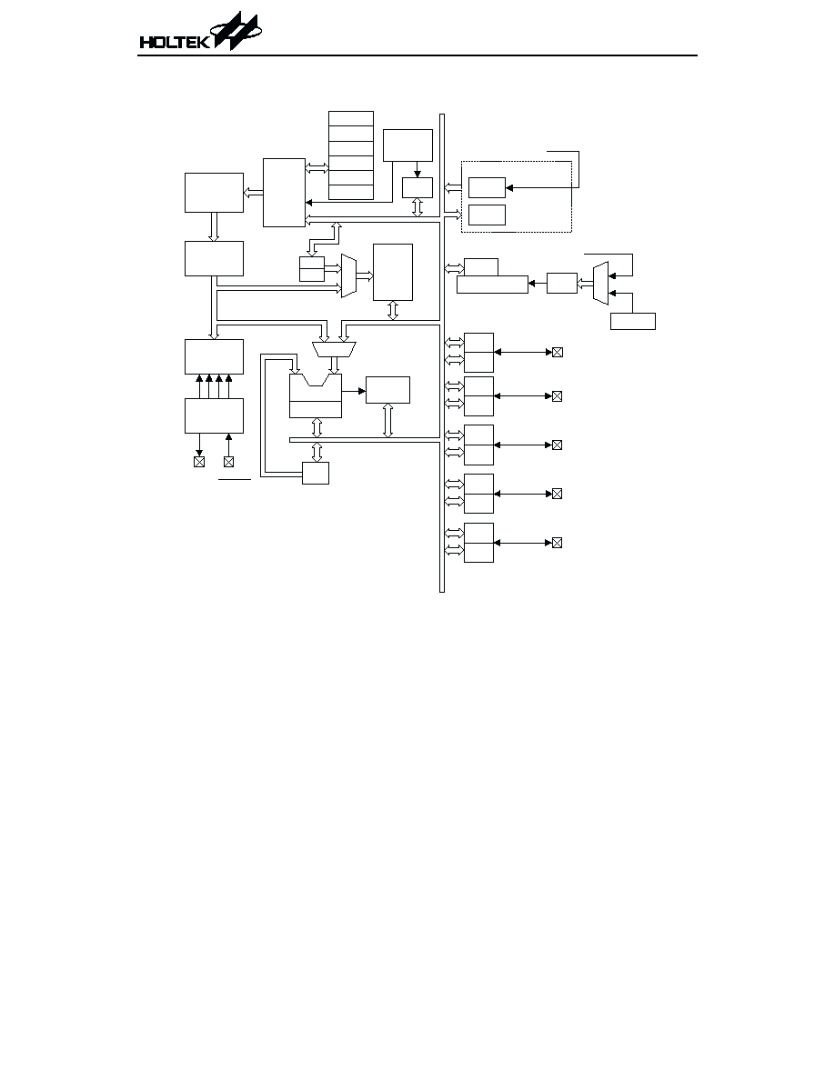
Block Diagram
HT82K68A
2
April 20, 2000
Preliminary
P r o g r a m
C o u n t e r
P r o g r a m
R O M
I n s t r u c t i o n
R e g i s t e r
I n s t r u c t i o n
D e c o d e r
T i m i n g
G e n e r a t o r
O S C 2
O S C 1
R E S E T
V D D
V S S
I n t e r r u p t
C i r c u i t
I N T C
M P 0
M P 1
M
U
X
M U X
D A T A
M e m o r y
A L U
S h i f t e r
S T A T U S
A C C
P C C
P C
P O R T C
P C 0 ~ P C 7
T M R
T M R C
S Y S C L K / 4
M
U
X
S Y S C L K / 4
W D T S
W D T P r e s c a l e r
W D T
R C O S C
8 b i t
P D C
P D
P O R T D
P D 0 ~ P D 7
P A C
P A
P O R T A
P A 0 ~ P A 7
P B C
P B
P O R T B
P B 0 ~ P B 7
S T A C K 2
S T A C K 3
S T A C K 0
S T A C K 1
S T A C K 4
S T A C K 5
P E C
P E
P E 0 ~ P E 4
P O R T E
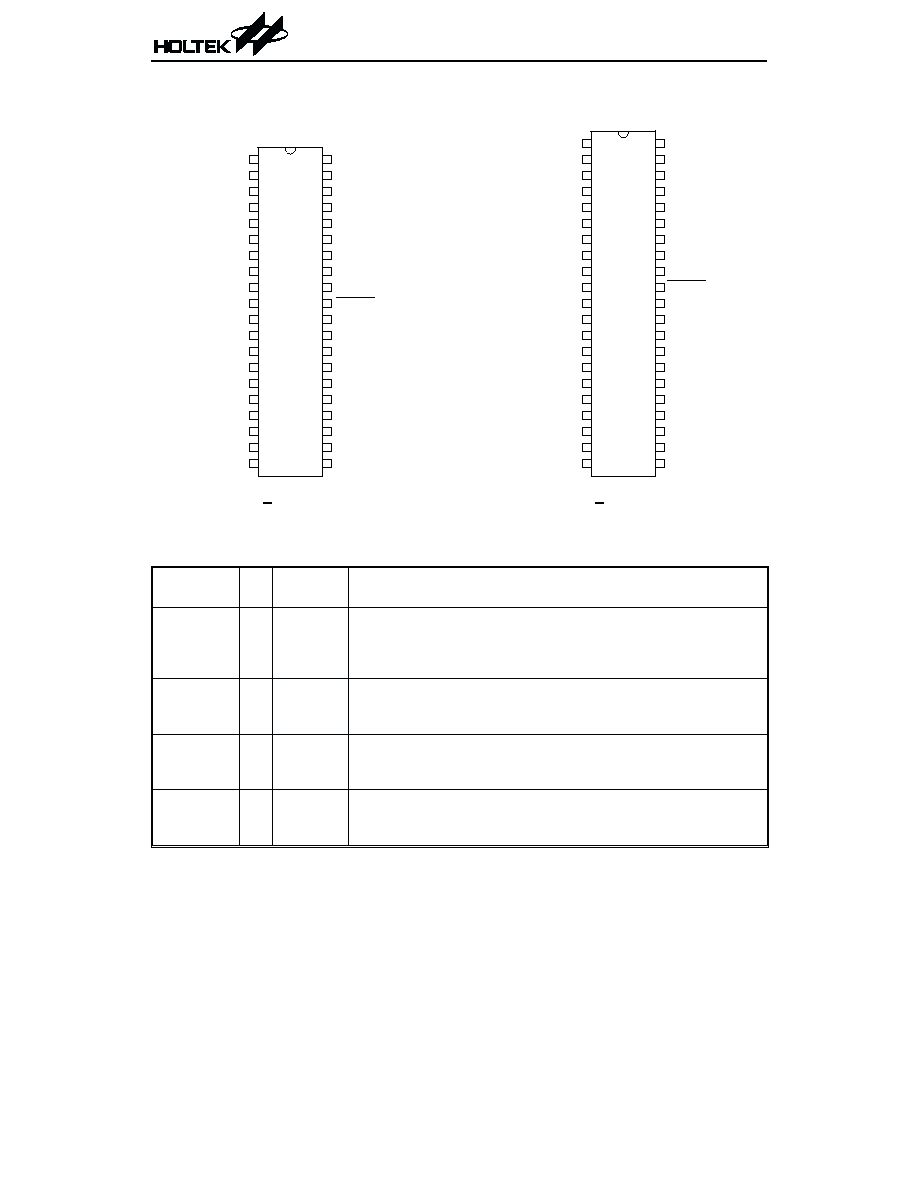
Pin Assignment
Pin Description
Pin Name I/O
Mask
Option
Description
PA0~PA7
I/O
Wake-up
Pull-high
or None
Bidirectional 8-bit input/output port. Each bit can be configured as
a wake-up input by mask option. Software* instructions determine
the CMOS output or schmitt trigger input with or without pull-high
resistor 12K.
PB0~PB7
I/O Pull-high
or None
Bidirectional 8-bit input/output port. Software* instructions deter-
mine the CMOS output or schmitt trigger input with or without
pull-high resistor.
PC0
I/O
Wake-up
Pull-high
or None
This pin is an I/O port. NMOS open drain output with pull-high re-
sistor and can be used as DATA or CLOCK line of PS2. This pin can
be configured as a wake-up input by mask option.
PC1
I/O
Wake-up
Pull-high
or None
This pin is an I/O port. NMOS open drain output with pull-high re-
sistor and can be used as DATA or CLOCK line of PS2. This pin can
be configured as a wake-up input by mask option.
HT82K68A
3
April 20, 2000
Preliminary
P B 6 ( R 6 )
P B 7 ( R 7 )
P A 4 ( C 4 )
P A 5 ( C 5 )
P A 6 ( C 6 )
P A 7 ( C 7 )
O S C 2
O S C 1
V D D
R E S E T
P E 4 ( C A P )
P D 3 ( R 1 1 )
P D 2 ( R 1 0 )
P D 1 ( R 9 )
P D 0 ( R 8 )
P C 7 ( R 1 7 )
P C 6 ( R 1 6 )
P C 5
P C 4
P C 3
P B 5 ( R 5 )
P B 4 ( R 4 )
P A 3 ( C 3 )
P A 2 ( C 2 )
P A 1 ( C 1 )
P A 0 ( C 0 )
P B 3 ( R 3 )
P B 2 ( R 2 )
P B 1 ( R 1 )
P B 0 ( R 0 )
P D 7 ( R 1 5 )
P D 6 ( R 1 4 )
P D 5 ( R 1 3 )
P D 4 ( R 1 2 )
V S S
P E 2 ( S C R )
P E 3 ( N U M )
P C 0 ( D A T A )
P C 1 ( C L K )
P C 2
4 0
3 9
3 8
3 7
3 6
3 5
3 4
3 3
3 2
3 1
3 0
2 9
2 8
2 7
2 6
2 5
2 4
2 3
2 2
2 1
1
2
3
4
5
6
7
8
9
1 0
1 1
1 2
1 3
1 4
1 5
1 6
1 7
1 8
1 9
2 0
H T 8 2 K 6 8 A
4 0 D I P
H T 8 2 K 6 8 A
4 2 D I P
4 2
4 1
4 0
3 9
3 8
3 7
3 6
3 5
3 4
3 3
3 2
3 1
3 0
2 9
2 8
2 7
2 6
2 5
2 4
2 3
2 2
1
2
3
4
5
6
7
8
9
1 0
1 1
1 2
1 3
1 4
1 5
1 6
1 7
1 8
1 9
2 0
2 1
P B 5 ( R 5 )
P B 4 ( R 4 )
P A 3 ( C 3 )
P A 2 ( C 2 )
P A 1 ( C 1 )
P A 0 ( C 0 )
P B 3 ( R 3 )
P B 2 ( R 2 )
P B 1 ( R 1 )
P B 0 ( R 0 )
P D 7 ( R 1 5 )
P D 6 ( R 1 4 )
P D 5 ( R 1 3 )
P D 4 ( R 1 2 )
V S S
P E 2 ( S C R )
P E 3 ( N U M )
P C 0 ( D A T A )
P C 1 ( C L K )
P C 2
P E 0
P B 6 ( R 6 )
P B 7 ( R 7 )
P A 4 ( C 4 )
P A 5 ( C 5 )
P A 6 ( C 6 )
P A 7 ( C 7 )
O S C 2
O S C 1
V D D
R E S E T
P E 4 ( C A P )
P D 3 ( R 1 1 )
P D 2 ( R 1 0 )
P D 1 ( R 9 )
P D 0 ( R 8 )
P C 7 ( R 1 7 )
P C 6 ( R 1 6 )
P C 5
P C 4
P C 3
P E 1
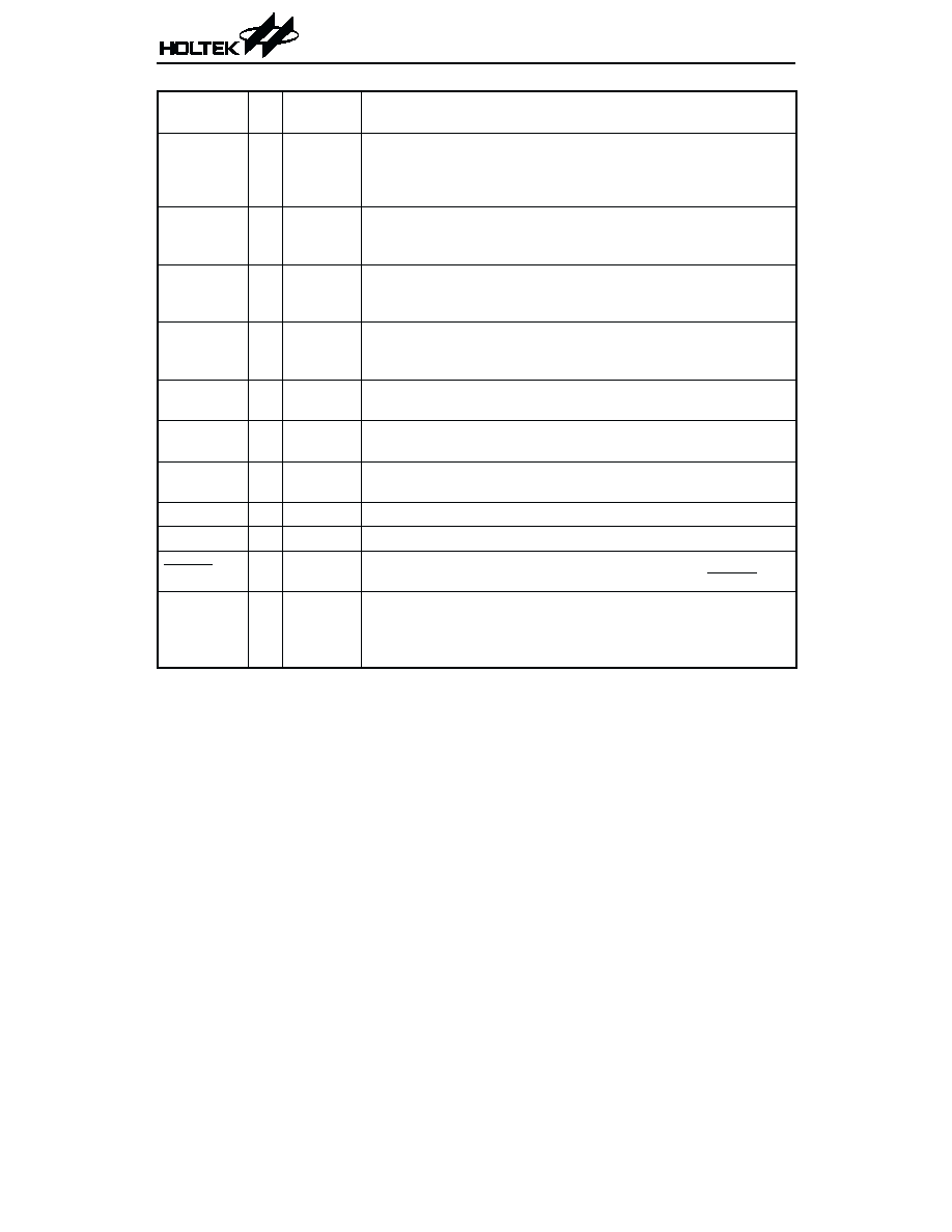
Pin Name I/O
Mask
Option
Description
PC2~PC3
I/O
Wake-up
Pull-high
or None
Bidirectional 2-bit input/output port. Each bit can be configured as
a wake-up input by mask option. Software* instructions determine
the CMOS output or schmitt trigger input with or without
pull-high resistor.
PC4~PC7
I/O Pull-high
or None
Bidirectional 4-bit input/output port. Software* instructions deter-
mine the CMOS output or schmitt trigger input with or without
pull-high resistor.
PD0~PD7
I/O Pull-high
or None
Bidirectional 8-bit input/output port. Software* instructions deter-
mine the CMOS output or schmitt trigger input with or without
pull-high resistor.
PE0~PE1
I/O Pull-high
or None
Bidirectional input/output port. Software* instruction determine
the CMOS output or schmitt trigger input with or without
pull-high resistor.
PE2
O
This pin is an NMOS output structure. The pad can function as
LED (SCR) drivers for the keyboard. I
OL
=14mA, @V
OL
=3.2V
PE3
O
This pin is an NMOS output structure. The pad can function as
LED (NUM) drivers for the keyboard. I
OL
=14mA, @V
OL
=3.2V
PE4
O
This pin is an NMOS output structure. The pad can function as
LED (CAP) drivers for the keyboard. I
OL
=14mA, @V
OL
=3.2V
VDD
¾
¾
Positive power supply
VSS
¾
¾
Negative power supply, ground
RESET
I
¾
Chip reset input. Active low. Built-in power-on reset circuit to reset
the entire chip. Chip can also be externally reset via RESET pin
OSC1
OSC2
I
O
Crystal or
RC
OSC1, OSC2 are connected to an RC network or a crystal for the in-
ternal system clock. In the case of RC operation, OSC2 is the output
terminal for the 1/4 system clock; A 110kW resistor is connected to
OSC1 to generate a 2 MHZ frequency.
Note: *: Software means the HT-IDE (Holtek Integrated Development Environment) can be con-
figured by mask option.
Absolute Maximum Ratings
Supply Voltage .............................-0.3V to 5.5V
Storage Temperature ................-50°C to 125°C
Input Voltage ................V
SS
-0
.
3V to V
DD
+0.3V
Operating Temperature .............-25°C to 70°C
Note: These are stress ratings only. Stresses exceeding the range specified under ²Absolute Maxi-
mum Ratings² may cause substantial damage to the device. Functional operation of this device
at other conditions beyond those listed in the specification is not implied and prolonged expo-
sure to extreme conditions may affect device reliability.
HT82K68A
4
April 20, 2000
Preliminary
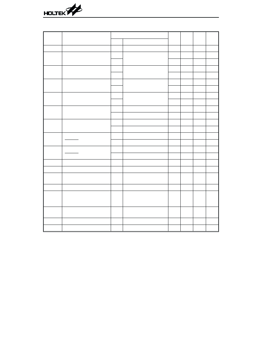
D.C. Characteristics
Ta=25°C
Symbol
Parameter
Test Conditions
Min. Typ. Max. Unit
V
DD
Conditions
V
DD
Operating Voltage
¾
¾
2.2
¾
5.5
V
I
DD1
Operating Current
(Crystal OSC)
3V
No load, f
SYS
= 2MHz
¾
0.7
1.5
mA
5V
¾
2
5
mA
I
DD2
Operating Current
(RC OSC)
3V
No load, f
SYS
= 2MHz
¾
0.5
1
mA
5V
¾
2
5
mA
I
STB1
Standby Current
(WDT enabled)
3V
No load, system HALT
¾
¾
8
mA
5V
¾
¾
15
mA
I
STB2
Standby Current
(WDT Disabled)
3V
No load, system HALT
¾
¾
3
mA
5V
¾
¾
6
mA
V
IL
Input Low Voltage for
I/O Ports
3V
¾
0
¾
0.9
V
5V
¾
0
¾
1.5
V
V
IH
Input High Voltage for
I/O Ports
3V
¾
2.1
¾
3
V
5V
¾
3.5
¾
5
V
V
IL1
Input Low Voltage
(RESET)
3V
¾
0
¾
0.7
V
5V
¾
0
¾
1.3
V
V
IH1
Input High Voltage
(RESET)
3V
¾
2.4
¾
3
V
5V
¾
4.0
¾
5
V
I
OL
I/O Port Sink Current
5V V
OL
= 0.5V
7
12
¾
mA
I
OH
I/O Port Source Current
5V V
OH
= 4.5V
-2.5 -4.5
¾
mA
I
LED
LED Sink Current
(SCR, NUM, CAP)
5V V
OL
=3.2V
10
14
18
mA
t
POR
Power-on Reset Time
5V
¾
120
150
180
ms
R
PH
Internal Pull-high
Resistance of PA, PB, PC,
PD, PE Port
5V
¾
5
12
20
kW
R
PH1
Internal Pull-high
Resistance of DATA, CLK 5V
¾
2
4.7
8
kW
Df/f
Frequency Variation
5V Crystal
¾
¾
±1
%
Df/f1
Frequency Variation
5V RC
¾
¾
±10
%
HT82K68A
5
April 20, 2000
Preliminary
Document Outline
- þÿ
- þÿ
- þÿ
- þÿ
- þÿ
- þÿ
- þÿ
- þÿ
- þÿ
- þÿ
- þÿ
- þÿ