 | ÐлекÑÑоннÑй компоненÑ: HT82J97E | СкаÑаÑÑ:  PDF PDF  ZIP ZIP |
Äîêóìåíòàöèÿ è îïèñàíèÿ www.docs.chipfind.ru
HT82J97E
USB Joystick Encoder 8-Bit OTP MCU
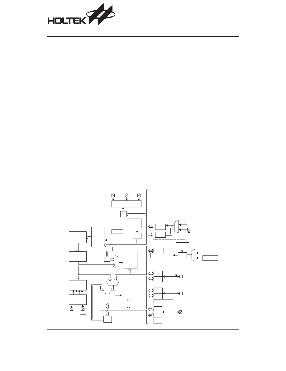
Block Diagram
Rev. 1.30
1
May 10, 2004
General Description
The USB MCU OTP body is suitable for USB mouse
and USB joystick devices. It consists of a Holtek high
performance 8-bit MCU core for control unit, built-in
USB SIE, 2K
´14 EPROM and 96 bytes data RAM.
Features
·
Flexible total solution for applications that combine
PS/2 and low-speed USB interface, such as mice,
joysticks, and many others
·
USB Specification Compliance
-
Conforms to USB specification V1.1
-
Conforms to USB HID specification V1.1
·
Supports 1 Low-speed USB control endpoint and 1
interrupt endpoint
·
Each endpoint has 8
´8 bytes FIFO
·
Integrated USB transceiver
·
3.3V regulator output
·
External 6MHz or 12MHz ceramic resonator or crys-
tal
·
8-bit RISC microcontroller, with 2K
´14 EPROM
(000H~7FFH)
·
96 bytes RAM (20H~7FH)
·
6MHz/12MHz internal CPU clock
·
4-level stacks
·
Two 8-bit indirect addressing registers
·
One 16-bit programmable timer counter with over-
flow interrupt (shared with PA7, vector 0CH)
·
One USB interrupt input (vector 04H)
·
HALT function and wake-up feature reduce power
consumption
·
PA0~PA7 support wake-up function
·
Internal Power-On reset (POR)
·
Watchdog Timer (WDT)
·
20 I/O ports (including 2-PWM output, PC2, PC3)
·
2 PWM output (PC2, PC3)
·
Can produce PWM frequency range from 23Hz to
23kHz
·
Built-in 8-bit Analog-to-Digital Converter, (6-channel
for internal mode (PB0~PB5), 6-channel for external
mode with VHL (PB7) and VRL (PB6))
·
20/28-pin SOP package
O S C 2
O S C 1
R E S
V D D
M U X
T M R 0 C
T M R 0
V S S
P r o g r a m
R O M
P r o g r a m
C o u n t e r
I n t e r r u p t
C i r c u i t
S T A C K
I N T C
D A T A
M e m o r y
I n s t r u c t i o n
R e g i s t e r
M
U
X
I n s t r u c t i o n
D e c o d e r
S T A T U S
A L U
S h i f t e r
T i m i n g
G e n e r a t o r
A C C
M
U
X
M P
S Y S C L K / 4
W D T S
W D T
W D T O S C
W D T P r e s c a l e r
M
U
X
E N / D I S
P B C
P O R T B
P B 0 / A N 0 ~ P B 5 / A N 5
P B 6 / V R L
P B 7 / V R H
P B
P A C
P O R T A
P A
P C
P O R T C
P C C
f
S Y S
/ 4
P A 7 / T M R
A / D C o n v e r t e r
U S B 1 . 1
P S 2
B P
U S B D + / C L K U S B D - / D A T A V 3 3 O
P W M
P C 0 ~ P C 1
P C 2 / P W M 1
P C 3 / P W M 2
P A 0 ~ P A 6
P A 7 / T M R
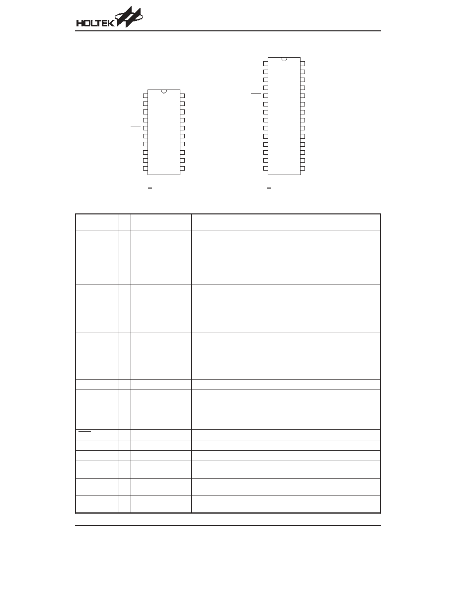
Pin Assignment
Pin Description
Pin Name
I/O
ROM Code
Option
Description
PA0~PA7
I/O
Pull-low
Pull-high
Wake-up
CMOS/NMOS/PMOS
Bidirectional 8-bit input/output port. Each bit can be configured as a
wake-up input by ROM code option. The input or output mode is con-
trolled by PAC (PA control register).
Pull-high resistor options: PA0~PA7
Pull-low resistor options: PA0~PA3
CMOS/NMOS/PMOS options: PA0~PA7
Wake-up options: PA0~PA7
PB0/AN0
PB1/AN1
PB2/AN2
PB3/AN3
PB5/AN5
PB6/VRL
I/O
Pull-high
Analog input
Bidirectional 8-bit input/output port. Software instructions determine the
CMOS output or Schmitt trigger input with pull-high resistor (determined
by pull-high options).
The PB can be used as analog input of the analog to digital converter
(determined by options).
Pull-low resistor for options: PB2, PB3
PB4/AN4
PB7/VRH
I/O
Pull-high
Analog input
Wake-up
Bidirectional 8-bit input/output port. Software instructions determine the
CMOS output or Schmitt trigger input with pull-high resistor (determined
by pull-high options).
The PB can be used as analog input of the analog to digital converter
(determined by options).
Wake-up options: PB4, PB7
VSS
¾
¾
Negative power supply, ground
PC0~PC3
I/O
Pull-high
Bidirectional I/O lines. Software instructions determine the CMOS out-
put or Schmitt trigger input with pull-high resistor (determined by
pull-high options).
PC2 can be used as PWM1 output
PC3 can be used as PWM2 output
RES
I
¾
Schmitt trigger reset input. Active low.
VDD
¾
¾
Positive power supply
V33O
O
¾
3.3V regulator output
USBD+/CLK
I/O
¾
USBD+ or PS2 CLK I/O line
USB or PS2 function is controlled by software control register
USBD-/DATA
I/O
¾
USBD- or PS2 DATA I/O line
USB or PS2 function is controlled by software control register
OSCI
OSCO
I
O
¾
OSCI, OSCO are connected to a 6MHz or 12MHz crystal/resonator (de-
termined by software instructions) for the internal system clock.
HT82J97E
Rev. 1.30
2
May 10, 2004
2 0
1 9
1 8
1 7
1 6
1 5
1 4
1 3
1 2
1 1
1
2
3
4
5
6
7
8
9
1 0
H T 8 2 J 9 7 E
2 0 S O P - A
V S S
V 3 3 O
U S B D + / C L K
U S B D - / D A T A
R E S
P A 0
P A 1
P B 2
P B 3
P B 4
O S C I
O S C O
V D D
P A 7
P A 6
P A 5
P A 4
P A 3
P A 2
P B 7
2 8
2 7
2 6
2 5
2 4
2 3
2 2
2 1
2 0
1 9
1 8
1 7
1 6
1 5
1
2
3
4
5
6
7
8
9
1 0
1 1
1 2
1 3
1 4
H T 8 2 J 9 7 E
2 8 S O P - A
V S S
V 3 3 O
U S B D + / C L K
U S B D - / D A T A
R E S
P A 0
P A 1
P C 0
P C 1
P B 0 / A N 0
P B 1 / A N 1
P B 2 / A N 2
P B 3 / A N 3
P B 4 / A N 4
O S C I
O S C O
V D D
P C 3 / P W M 2
P C 2 / P W M 1
P A 7
P A 6
P A 5
P A 4
P A 3
P A 2
P B 7 / V R H
P B 6 / V R L
P B 5 / A N 5

Absolute Maximum Ratings
Supply Voltage ...........................V
SS
-0.3V to V
SS
+6.0V
Storage Temperature ............................
-50°C to 125°C
Input Voltage..............................V
SS
-0.3V to V
DD
+0.3V
Operating Temperature...............................0
°C to 70°C
Note: These are stress ratings only. Stresses exceeding the range specified under
²Absolute Maximum Ratings² may
cause substantial damage to the device. Functional operation of this device at other conditions beyond those
listed in the specification is not implied and prolonged exposure to extreme conditions may affect device reliabil-
ity.
D.C. Characteristics
Ta=25
°C
Symbol
Parameter
Test Conditions
Min.
Typ.
Max.
Unit
V
DD
Conditions
V
DD
Operating Voltage
¾
¾
4
¾
5.5
V
I
DD
Operating Current (6MHz Crystal)
5V
No load, f
SYS
=6MHz
¾
7
9
mA
I
STB
Standby Current
5V
No load, system HALT
¾
300
500
mA
V
IL1
Input Low Voltage for I/O Ports
5V
¾
0
¾
0.8
V
V
IH1
Input High Voltage for I/O Ports
5V
¾
2
¾
5
V
V
IL2
Input Low Voltage (RES)
5V
¾
0
¾
0.4V
DD
V
V
IH2
Input High Voltage (RES)
5V
¾
0.9V
DD
¾
V
DD
V
I
OL
Output Sink Current for Other Ports
PA0~PA7, PB0~PB7 and PC0~PC3
5V
V
OL
=0.4V
2
4
¾
mA
I
OH
Output Port Source Current
5V
V
OL
=3.4V
-2.5
-4
¾
mA
R
PD
Pull-down Resistance for PA0~PA3, PB2
and PB3
5V
¾
10
30
50
k
W
R
PH1
Pull-high Resistance for CLK and DATA
¾
¾
2
4.7
6
k
W
R
PH2
Pull-high Resistance for PA0~PA7,
PB0~PB7 and PC0~PC3
¾
¾
30
50
70
k
W
V
LVR
Low Voltage Reset
5V
¾
2.4
2.7
3
V
A.C. Characteristics
Ta=25
°C
Symbol
Parameter
Test Conditions
Min.
Typ.
Max.
Unit
V
DD
Conditions
f
SYS
System Clock (Crystal OSC)
5V
¾
6
¾
12
MHz
f
RCSYS
RC Clock with 8-bit Prescaler Register
5V
¾
0
32
¾
kHz
t
WDT
Watchdog Time-out Period (System Clock)
¾ Without WDT prescaler 1024
¾
¾
t
RCSYS
t
RF
USBD+, USBD- Rising & falling Time
¾
¾
75
¾
300
ns
t
SST
System Start-up Timer Period
¾ Wake-up from HALT
¾
1024
¾
t
SYS
t
OSC
Crystal Setup
¾
¾
¾
5
10
ms
f
PWM
PWM Cycle Frequency
¾ 6MHz or 12MHz
23
¾
2300
Hz
Note: Power-on period=t
WDT
+t
SST
+t
OSC
WDT Time-out in normal mode=1/f
RCSYS
´256´WDTS+t
WDT
WDT Time-out in HALT mode=1/f
RCSYS
´256´WDTS+t
SST
+t
OSC
HT82J97E
Rev. 1.30
3
May 10, 2004
HT82J97E
Rev. 1.30
4
May 10, 2004
Functional Description
Execution Flow
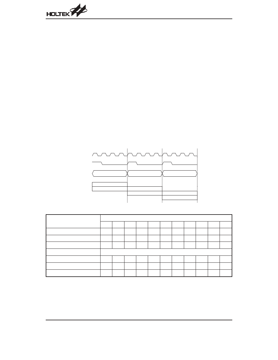
The system clock for the microcontroller is derived from
either 6MHz or 12MHz crystal oscillator, which used a
frequency that is determined by the SCLKSEL bit of the
SCC Register. The default system frequency is 12MHz.
The system clock is internally divided into four non-
overlapping clocks. One instruction cycle consists of
four system clock cycles.
Instruction fetching and execution are pipelined in such
a way that a fetch takes an instruction cycle while de-
coding and execution takes the next instruction cycle.
However, the pipelining scheme causes each instruc-
tion to be effectively executed in a cycle. If an instruction
changes the program counter, two cycles are required to
complete the instruction.
Program Counter
- PC
The program counter (PC) controls the sequence in
which the instructions stored in the program ROM are
executed and its contents specify a full range of pro-
gram memory.
After accessing a program memory word to fetch an in-
struction code, the contents of the program counter are
incremented by one. The program counter then points to
the memory word containing the next instruction code.
When executing a jump instruction, conditional skip ex-
ecution, loading to the PCL register, performing a sub-
routine call or return from subroutine, initial reset,
internal interrupt, external interrupt or return from inter-
rupts, the PC manipulates the program transfer by load-
ing the address corresponding to each instruction.
The conditional skip is activated by instructions. Once
the condition is met, the next instruction, fetched during
the current instruction execution, is discarded and a
dummy cycle replaces it to get the proper instruction.
Otherwise proceed with the next instruction.
The lower byte of the program counter (PCL) is a read-
able and writeable register (06H). Moving data into the
PCL performs a short jump. The destination will be
within the current program ROM page.
When a control transfer takes place, an additional
dummy cycle is required.
T 1
T 2
T 3
T 4
T 1
T 2
T 3
T 4
T 1
T 2
T 3
T 4
F e t c h I N S T ( P C )
E x e c u t e I N S T ( P C - 1 )
F e t c h I N S T ( P C + 1 )
E x e c u t e I N S T ( P C )
F e t c h I N S T ( P C + 2 )
E x e c u t e I N S T ( P C + 1 )
P C
P C + 1
P C + 2
S y s t e m C l o c k
O S C 2 ( R C o n l y )
P C
Execution Flow
Mode
Program Counter
*10
*9
*8
*7
*6
*5
*4
*3
*2
*1
*0
Initial Reset
0
0
0
0
0
0
0
0
0
0
0
USB Interrupt
0
0
0
0
0
0
0
0
1
0
0
Timer/Event Counter Overflow
0
0
0
0
0
0
0
1
1
0
0
Skip
PC+2
Loading PCL
*10
*9
*8
@7
@6
@5
@4
@3
@2
@1
@0
Jump, Call Branch
#10
#9
#8
#7
#6
#5
#4
#3
#2
#1
#0
Return from Subroutine
S10
S9
S8
S7
S6
S5
S4
S3
S2
S1
S0
Program Counter
Note: *10~*0: Program counter bits
S10~S0: Stack register bits
#10~#0: Instruction code bits
@7~@0: PCL bits
HT82J97E
Rev. 1.30
5
May 10, 2004
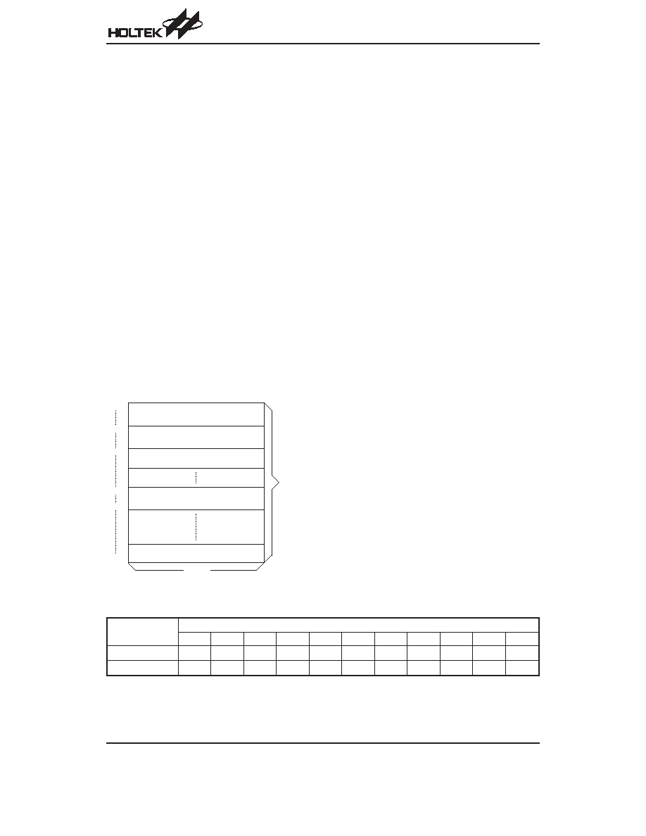
Program Memory
- ROM
The program memory is used to store the program in-
structions which are to be executed. It also contains
data, table, and interrupt entries, and is organized into
2048
´14 bits, addressed by the program counter and ta-
ble pointer.
Certain locations in the program memory are reserved
for special usage:
·
Location 000H
This area is reserved for program initialization. After a
chip reset, the program always begins execution at lo-
cation 000H.
·
Location 004H
This area is reserved for the USB interrupt service
program. If the USB interrupt is activated, the interrupt
is enabled and the stack is not full, the program begins
execution at location 004H.
·
Location 00CH
This location is reserved for the Timer/Event Counter
interrupt service program. If a timer interrupt results
from a Timer/Event Counter overflow, and the inter-
rupt is enabled and the stack is not full, the program
begins execution at location 00CH.
·
Table location
Any location in the program memory can be used as
look-up tables. There are three method to read the
ROM data by two table read instructions:
²TABRDC²
and
²TABRDL², transfer the contents of the
lower-order byte to the specified data memory, and
the higher-order byte to TBLH (08H).
The three methods are shown as follows:
¨
The instructions
²TABRDC [m]² (the current page,
one page=256words), where the table locations is
defined by TBLP (07H) in the current page. And the
ROM code option TBHP is disabled (default).
¨
The instructions
²TABRDC [m]², where the table lo-
cations is defined by registers TBLP (07H) and
TBHP (01FH). And the ROM code option TBHP is
enabled.
¨
The instructions
²TABRDL [m]², where the table lo-
cations is defined by Registers TBLP (07H) in the
last page (0700H~07FFH).
Only the destination of the lower-order byte in the ta-
ble is well-defined, the other bits of the table word are
transferred to the lower portion of TBLH, and the re-
maining 1-bit words are read as
²0². The Table
Higher-order byte register (TBLH) is read only. The ta-
ble pointer (TBLP, TBHP) is a read/write register (07H,
1FH), which indicates the table location. Before ac-
cessing the table, the location must be placed in the
TBLP and TBHP (If the OTP option TBHP is disabled,
the value in TBHP has no effect). The TBLH is read
only and cannot be restored. If the main routine and
the ISR (Interrupt Service Routine) both employ the
table read instruction, the contents of the TBLH in the
main routine are likely to be changed by the table read
instruction used in the ISR. Errors can occur. In other
words, using the table read instruction in the main rou-
tine and the ISR simultaneously should be avoided.
However, if the table read instruction has to be applied
in both the main routine and the ISR, the interrupt
should be disabled prior to the table read instruction. It
will not be enabled until the TBLH has been backed
up. All table related instructions require two cycles to
complete the operation. These areas may function as
normal program memory depending on the require-
ments.
Once TBHP is enabled, the instruction
²TABRDC [m]²
reads the ROM data as defined by TBLP and TBHP
value. Otherwise, the ROM code option TBHP is dis-
abled, the instruction
²TABRDC [m]² reads the ROM
data as defined by TBLP and the current program
counter bits.
1 4 B i t s
7 F F H
n F F H
P r o g r a m
M e m o r y
L o o k - u p T a b l e ( 2 5 6 W o r d s )
L o o k - u p T a b l e ( 2 5 6 W o r d s )
N o t e : n r a n g e s f r o m 0 t o 7
0 0 C H
n 0 0 H
D e v i c e I n i t i a l i z a t i o n P r o g r a m
U S B I n t e r r u p t S u b r o u t i n e
0 0 4 H
0 0 0 H
T i m e r / E v e n t C o u n t e r
I n t e r r u p t S u b r o u t i n e
Program Memory
Instruction
Table Location
*10
*9
*8
*7
*6
*5
*4
*3
*2
*1
*0
TABRDC [m]
P10
P9
P8
@7
@6
@5
@4
@3
@2
@1
@0
TABRDL [m]
1
1
1
@7
@6
@5
@4
@3
@2
@1
@0
Table Location
Note: *10~*0: Table location bits
P10~P8: Current program counter bits when TBHP is disabled
@7~@0: TBLP bits
TBHP register bit2~bit0 when TBHP is enabled
Document Outline
- þÿ
- þÿ
- þÿ
- þÿ
- þÿ
- þÿ
- þÿ
- þÿ
- þÿ
- þÿ
- þÿ
- þÿ
- þÿ
- þÿ
- þÿ