 | –≠–ª–µ–∫—Ç—Ä–æ–Ω–Ω—ã–π –∫–æ–º–ø–æ–Ω–µ–Ω—Ç: HT36M4 | –°–∫–∞—á–∞—Ç—å:  PDF PDF  ZIP ZIP |
Document Outline
- ˛ˇ
- ˛ˇ
- ˛ˇ
- ˛ˇ
- ˛ˇ
- ˛ˇ
- ˛ˇ
- ˛ˇ
- ˛ˇ
- ˛ˇ
- ˛ˇ
- ˛ˇ
- ˛ˇ
- ˛ˇ
- ˛ˇ

HT36M4
Music Synthesizer 8-Bit MCU
Block Diagram
Rev. 1.00
1
August 15, 2005
Features
∑
Operating voltage: 2.6V~5.0V
∑
Operating frequency:
-
Crystal: 8MHz~12MHz
-
RC: 11.059MHz
∑
12 bidirectional I/O lines
∑
Two 16-bit programmable timer/event counters with
overflow interrupts
∑
Watchdog Timer
∑
Built-in 8-bit MCU with 384
¥8 bits RAM
∑
Built-in 64K
¥16-bit ROM for program/data shared
∑
Mono 16-bit DAC
∑
One external interrupt
∑
Polyphonic up to 16 notes
∑
Independent pan and volume mix can be assigned to
each sound component
∑
Sampling rate of 44.1kHz as 11.059MHz for system
frequency
∑
Eight-level subroutine nesting
∑
HALT function and wake-up feature reduce power
consumption
∑
Bit manipulation instructions
∑
16-bit table read instructions
∑
Low voltage reset 2.2V
∑
63 powerful instructions
∑
All instructions in 1 or 2 machine cycles
∑
20-pin SOP/TSSOP package
General Description
The HT36M4 is an 8-bit high performance RISC
microcontroller specifically designed for music applica-
tions. It provides an 8-bit MCU and a 16 channel
wavetable synthesizer. The program ROM is composed
of both program control codes and wavetable voice
codes, which can easily be programmed.
The HT36M4 has a built-in 8-bit microprocessor with
64K
¥16 program ROM, 384¥8 data RAM, 12
bidirectional I/O, encapsulated in 20 TSSOP for applica-
tions where need tinny package such as ring tone gen-
erator for CELLULAR/DECT/CORDLESS PHONES.
8 - B i t
M C U
6 4 K ¥ 1 6 - b i t
R O M
3 8 4 ¥ 8
R A M
M u l t i p l i e r / P h a s e
G e n e r a l
P A 0 ~ P A 7
P B 0 ~ P B 3
O S C 1
O S C 2
R E S
1 6 - B i t
D A C
V D D
V S S
V D D A
A U D I O
P F 0 ~ 2
V S S A
I N T
Technical Document
∑
Tools Information
∑
FAQs
∑
Application Note
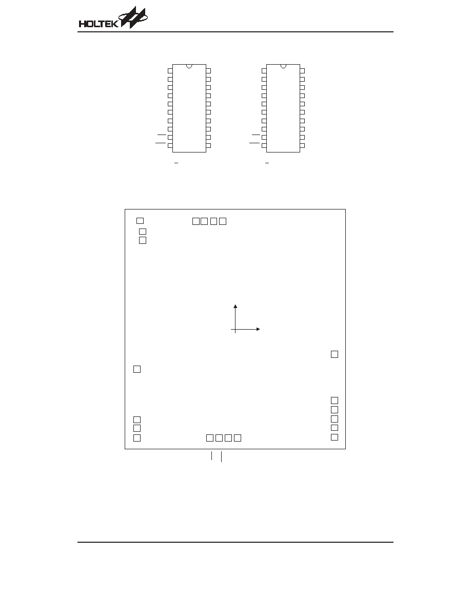
Pin Assignment
Pad Assignment
Chip size: 2595
¥2815 (mm)
2
* The IC substrate should be connected to VSS in the PCB layout artwork.
HT36M4
Rev. 1.00
2
August 15, 2005
A U D I O
V D D A
V S S / V S S A
O S C 2
O S C 1
V D D
I N T
R E S
P A 7
P A 6
P A 1
P A 2
P A 3
P A 4
P A 5
P A 0
P B 3
P B 2
P B 1
P B 0
2 0
1 9
1 8
1 7
1 6
1 5
1 4
1 3
1 2
1 1
1
2
3
4
5
6
7
8
9
1 0
H T 3 6 M 4
2 0 T S S O P - A
A U D I O
V D D A
V S S / V S S A
O S C 2
O S C 1
V D D
I N T
R E S
P A 7
P A 6
P A 1
P A 2
P A 3
P A 4
P A 5
P A 0
P B 3
P B 2
P B 1
P B 0
2 0
1 9
1 8
1 7
1 6
1 5
1 4
1 3
1 2
1 1
1
2
3
4
5
6
7
8
9
1 0
H T 3 6 M 4
2 0 S O P - A
1
2
3
2 1 2 0 1 9 1 8
4
5
6
7
8
9
1 0 1 1
1 2
1 3
1 4
1 5
1 6
1 7
( 0 , 0 )
A U D I O
V D D A
V S S A
V S S
O S C 2
O S C 1
V D D
I
N
T
R
E
S
P
A
7
P
A
6
P A 1
P A 2
P A 3
P A 4
P A 5
P A 0
P
B
3
P
B
2
P
B
1
P
B
0

Pad Coordinates
Unit:
mm
Pad No.
X
Y
Pad No.
X
Y
1
-1108.950
1261.050
12
1146.750
-1250.000
2
-1076.600
1135.900
13
1146.750
-1139.400
3
-1076.600
1030.900
14
1146.750
-1039.400
4
-1146.750
-460.600
15
1146.750
-928.800
5
-1146.750
-1044.234
16
1146.750
-828.800
6
-1146.750
-1147.786
17
1146.750
-286.200
7
-1146.750
-1260.200
18
-153.300
1256.550
8
-292.374
-1256.550
19
-253.300
1256.550
9
-187.326
-1256.550
20
-363.900
1256.550
10
-85.550
-1256.550
21
-463.900
1256.550
11
25.050
-1256.550
Pad Description
Pad No.
Pad Name
I/O
Internal
Connection
Function
1
AUDIO
O
æ
Audio output
2, 3
VDDA, VSSA
æ
æ
DAC power supply
7, 4
VDD, VSS
æ
æ
Digital power supply, ground
5
OSC2
O
æ
X
OUT
or 1/4 system frequency in R mode
6
OSC1
I
X
¢tal/Resistor X
IN
for X
¢tal or R
OSC
in for resistor by mask option
8
INT
I
Pull-High
External interrupt
9
RES
I
æ
Reset input, active low
17~10
PA7~PA0
I/O
Pull-High
or None
Bidirectional 8-bit Input/Output port, wake-up by mask option
21~18
PB0~PB3
I/O
Pull-High
or None
Bidirectional 8-bit input/output port
Absolute Maximum Ratings
Supply Voltage ..........................V
SS
-0.3V to V
SS
+5.5V
Storage Temperature ...........................
-50∞C to 125∞C
Input Voltage .............................V
SS
-0
.
3V to V
DD
+0.3V
Operating Temperature ..........................
-25∞C to 70∞C
Note: These are stress ratings only. Stresses exceeding the range specified under
≤Absolute Maximum Ratings≤ may
cause substantial damage to the device. Functional operation of this device at other conditions beyond those
listed in the specification is not implied and prolonged exposure to extreme conditions may affect device reliabil-
ity.
HT36M4
Rev. 1.00
3
August 15, 2005

D.C. Characteristics
Ta=25
∞C
Symbol
Parameter
Test Conditions
Min.
Typ.
Max.
Unit
V
DD
Conditions
V
DD
Operating Voltage
æ
æ
2.6
3.6
5
V
I
DD
Operating Current
3.6V
No load (OSC on)
æ
8
10
mA
I
STB
Standby Current
3.6V
æ
æ
1
3
mA
I
OH
I/O Ports Source Current
3.6V
æ
2
æ
æ
mA
I
OL
I/O Ports Sink Current
3.6V
æ
3
æ
æ
mA
V
IH
Input High Voltage
æ
æ
0.8V
DD
æ
V
DD
V
V
IL
Input Low Voltage
æ
æ
0
æ
0.2V
DD
V
A.C. Characteristics
Ta=25
∞C
Symbol
Parameter
Test Conditions
Min.
Typ.
Max.
Unit
V
DD
Conditions
f
OSC
System Frequency
5V
11.059MHz crystal
æ
11.059
æ
MHz
f
SYS
System Clock
5V
æ
4
æ
16
MHz
t
WDT
Watchdog Time-Out Period (RC)
æ
Without WDT prescaler
9
17
35
ms
t
RES
External Reset Low Pulse Width
æ
æ
1
æ
æ
ms
HT36M4
Rev. 1.00
4
August 15, 2005

HT36M4
Rev. 1.00
5
August 15, 2005
Functional Description
Execution Flow
The system clock for the HT36M4 is derived from either
a crystal or an RC oscillator. The oscillator frequency di-
vided by 2 is the system clock for the MCU and it is inter-
nally divided into four non-overlapping clocks. One
instruction cycle consists of four system clock cycles.
Instruction fetching and execution are pipelined in such
a way that a fetch takes one instruction cycle while de-
coding and execution takes the next instruction cycle.
However, the pipelining scheme causes each instruc-
tion to effectively execute in one cycle. If an instruction
changes the program counter, two cycles are required
to complete the instruction.
Program Counter
- PC
The 13-bit program counter (PC) controls the sequence
in which the instructions stored in program ROM are ex-
ecuted and its contents specify a maximum of 8192 ad-
dresses for each bank.
After accessing a program memory word to fetch an in-
struction code, the contents of the program counter are
incremented by one. The program counter then points
to the memory word containing the next instruction
code.
When executing a jump instruction, conditional skip ex-
ecution, loading PCL register, subroutine call, initial re-
set, internal interrupt, external interrupt or return from
subroutine, the PC manipulates the program transfer by
loading the address corresponding to each instruction.
The conditional skip is activated by instruction. Once the
condition is met, the next instruction, fetched during the
current instruction execution, is discarded and a dummy
cycle replaces it to retrieve the proper instruction. Other-
wise proceed with the next instruction.
The lower byte of the program counter (PCL) is a read-
able and writeable register (06H). Moving data into the
PCL performs a short jump. The destination will be
within 256 locations.
Once a control transfer takes place, an additional
dummy cycle is required.
Program ROM
HT36M4 provides 17 address lines WA16~WA0 to read
the Program ROM which is up to 1M bits, and is com-
monly used for the wavetable voice codes and the pro-
gram memory. It provides two address types, one type is
for program ROM, which is addressed by a bank pointer
PF2~PF0 and a 13-bit program counter PC12~PC0;
and the other type is for wavetable code, which is ad-
dressed by the start address ST15~ST0. On the pro-
gram type, WA16~WA0= PF2~PF0
¥2
13
+PC12~PC0.
O n t h e w a v e t a b l e R O M t y p e , WA 1 6 ~ WA 0 =
ST15~ST0
¥2
5
.
T 1
T 2
T 3
T 4
T 1
T 2
T 3
T 4
T 1
T 2
T 3
T 4
F e t c h I N S T ( P C )
E x e c u t e I N S T ( P C - 1 )
F e t c h I N S T ( P C + 1 )
E x e c u t e I N S T ( P C )
F e t c h I N S T ( P C + 2 )
E x e c u t e I N S T ( P C + 1 )
P C
P C + 1
P C + 2
S y s t e m C l o c k o f M C U
( S y s t e m C l o c k / 2 )
P C
Execution Flow
Mode
Program Counter
*12
*11
*10
*9
*8
*7
*6
*5
*4
*3
*2
*1
*0
Initial Reset
0
0
0
0
0
0
0
0
0
0
0
0
0
Timer/Event Counter 0 Overflow
0
0
0
0
0
0
0
0
0
1
0
0
0
Timer/Event Counter 1 Overflow
0
0
0
0
0
0
0
0
0
1
1
0
0
Skip
Program Counter+2
Loading PCL
*12
*11
*10
*9
*8
@7
@6
@5
@4
@3
@2
@1
@0
Jump, Call Branch
#12
#11
#10
#9
#8
#7
#6
#5
#4
#3
#2
#1
#0
Return From Subroutine
S12
S11
S10
S9
S8
S7
S6
S5
S4
S3
S2
S1
S0
Program Counter
Note:
*12~*0: Bits of Program Counter
@7~@0: Bits of PCL
#12~#0: Bits of Instruction Code
S12~S0: Bits of Stack Register
@7~@0: Bits of PCL