 | ÐлекÑÑоннÑй компоненÑ: HMC540LP3 | СкаÑаÑÑ:  PDF PDF  ZIP ZIP |
9_attenuator_smt_section.indd
9
A
T
T
E
N
U
A
T
O
R
S - SM
T
9 - 172
For price, delivery, and to place orders, please contact Hittite Microwave Corporation:
20 Alpha Road, Chelmsford, MA 01824 Phone: 978-250-3343 Fax: 978-250-3373
Order On-line at www.hittite.com
HMC540LP3
/
540LP3E
1 dB LSB GaAs MMIC 4-BIT DIGITAL
POSITIVE CONTROL ATTENUATOR, DC - 5.5 GHz
v00.0605
Functional Diagram
Electrical Specifications,
T
A
= +25° C, With Vdd = +5V & Vctl = 0/+5V (Unless Otherwise Noted)
The HMC540LP3 / HMC540LP3E is ideal for both RF
and IF applications:
· Cellular Infrastructure
· ISM, MMDS, WLAN, WiMAX, WiBro
· Microwave Radio & VSAT
· Test Equipment and Sensors
1 dB LSB Steps to 15 dB
+/- 0.2 dB Typical Step Error
Low Insertion Loss: 1.0 dB
High IP3: +50 dBm
Single Control Line Per Bit
TTL/CMOS Compatible Control
Single +5V Supply
3x3 mm SMT Package
The HMC540LP3 & HMC540LP3E are broadband
4-bit GaAs IC digital attenuators in low cost leadless
surface mount packages. This single positive control
line per bit digital attenuator utilizes off chip AC ground
capacitors for near DC operation, making it suitable for
a wide variety of RF and IF applications. Covering DC
to 5.5 GHz, the insertion loss is less than 1.0 dB typical.
The attenuator bit values are 1 (LSB), 2, 4 and 8 dB for
a total attenuation of 15 dB. Attenuation accuracy is
excellent at ± 0.2 dB typical step error. The attenuator
also features a IIP3 of +50 dBm. Four TTL/CMOS
control inputs are used to select each attenuation
state. A single Vdd bias of +5V is required.
Parameter
Frequency (GHz)
Min.
Typ.
Max.
Units
Insertion Loss
DC - 2.0 GHz
2.0 - 3.0 GHz
3.0 - 4.0 GHz
4.0 -5.5 GHz
0.8
1.0
1.3
2.2
1.1
1.3
1.6
2.6
dB
dB
dB
dB
Attenuation Range
DC - 5.5 GHz
15
dB
Return Loss (RF1 & RF2, All Atten. States)
DC - 3.5 GHz
3.5 - 5.5 GHz
20
15
dB
dB
Attenuation Accuracy:
(Referenced to Insertion Loss)
All States
DC - 1.0 GHz
1.0 - 4.0 GHz
4.0 - 5.0 GHz
5.0 - 5.5 GHz
± (0.2 + 2% of Atten. Setting) Max.
± (0.2 + 3% of Atten. Setting) Max.
± (0.3 + 5% of Atten. Setting) Max.
± (0.4 + 8% of Atten. Setting) Max.
dB
dB
dB
dB
Input Power for 0.1 dB Compression
0.1 - 5.5 GHz
27
dBm
Input Third Order Intercept Point
(Two-Tone Input Power= 0 dBm Each Tone)
REF - 4 dB States
5 - 15 dB States
0.1 - 5.5 GHz
50
45
dBm
dBm
Switching Characteristics
tRISE, tFALL (10/90% RF)
tON, tOFF (50% CTL to 10/90% RF)
DC -5.5 GHz
95
100
ns
ns
Typical Applications
Features
General Discription
9
A
T
T
E
N
U
A
T
O
R
S - SM
T
9 - 173
For price, delivery, and to place orders, please contact Hittite Microwave Corporation:
20 Alpha Road, Chelmsford, MA 01824 Phone: 978-250-3343 Fax: 978-250-3373
Order On-line at www.hittite.com
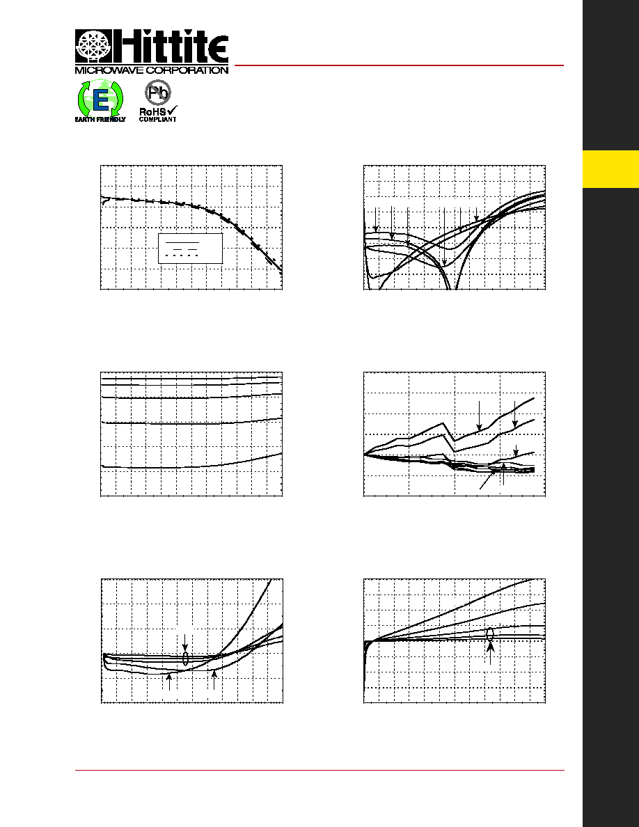
Return Loss RF1, RF2
(Only Major States are Shown)
Insertion Loss
Normalized Attenuation
(Only Major States are Shown)
Bit Error vs. Frequency
(Only Major States are Shown)
Relative Phase vs. Frequency
(Only Major States are Shown)
Bit Error vs. Attenuation State
-3
-2.5
-2
-1.5
-1
-0.5
0
0
0.5
1
1.5
2
2.5
3
3.5
4
4.5
5
5.5
6
+25 C
+85 C
-40 C
INSERTION LOSS (dB)
FREQUENCY (GHz)
-1
-0.5
0
0.5
1
1.5
2
0
4
8
12
16
BI
T ERROR (dB)
ATTENUATION STATE (dB)
5 GHz
5.5 GHz
1 GHz
100 MHz
4 GHz
-20
-16
-12
-8
-4
0
0
0.5
1
1.5
2
2.5
3
3.5
4
4.5
5
5.5
6
NORMALI
ZED ATTENUATI
ON (dB)
FREQUENCY (GHz)
-1
-0.5
0
0.5
1
1.5
0
0.5
1
1.5
2
2.5
3
3.5
4
4.5
5
5.5
6
BIT ERROR (dB)
FREQUENCY (GHz)
8 dB
15 dB
1-4 dB
-40
-30
-20
-10
0
10
20
30
40
0
0.5
1
1.5
2
2.5
3
3.5
4
4.5
5
5.5
6
RELATIVE PHASE (deg)
FREQUENCY (GHz)
15 dB
8 dB
1-4 dB
-40
-35
-30
-25
-20
-15
-10
-5
0
0
0.5
1
1.5
2
2.5
3
3.5
4
4.5
5
5.5
6
RETURN LOSS (dB)
FREQUENCY (GHz)
1 dB 2 dB
4 dB
I.L.dB
8 dB 15 dB
HMC540LP3
/
540LP3E
1 dB LSB GaAs MMIC 4-BIT DIGITAL
POSITIVE CONTROL ATTENUATOR, DC - 5.5 GHz
v00.0605
9
A
T
T
E
N
U
A
T
O
R
S - SM
T
9 - 174
For price, delivery, and to place orders, please contact Hittite Microwave Corporation:
20 Alpha Road, Chelmsford, MA 01824 Phone: 978-250-3343 Fax: 978-250-3373
Order On-line at www.hittite.com
Truth Table
Control Voltage
Bias Voltage & Current
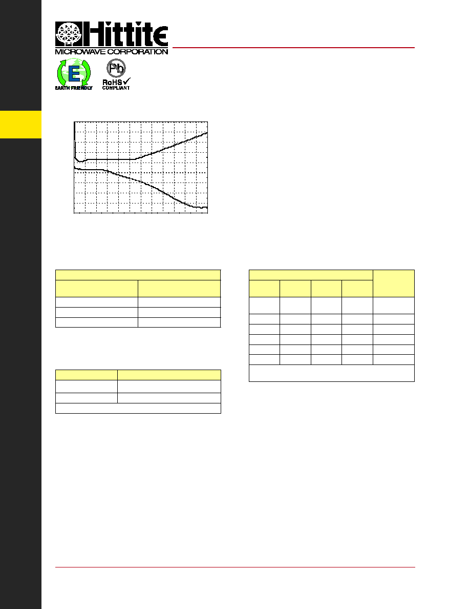
Worst Case Step Error
Between Successive Attenuation States
Vdd = +5.0 Vdc ± 10%
Vdd
(VDC)
Idd (Typ.)
(mA)
+4.5
3.0
+5.0
3.2
+5.5
3.4
State
Bias Condition
Low
0 to +0.8V @ -5 uA Typ.
High
+2.0 to + 5.0 Vdc @ 40 uA Typ.
Note: Vdd = +5V
Control Voltage Input
Attenuation
State
RF1 - RF2
V1
8 dB
V2
4 dB
V3
2 dB
V4
1 dB
High
High
High
High
Reference
I.L.
High
High
High
Low
1 dB
High
High
Low
High
2 dB
High
Low
High
High
4 dB
Low
High
High
High
8 dB
Low
Low
Low
Low
15 dB
Any combination of the above states will provide an attenuation
approximately equal to the sum of the bits selected.
-0.5
-0.4
-0.3
-0.2
-0.1
0
0.1
0.2
0.3
0.4
0
0.5
1
1.5
2
2.5
3
3.5
4
4.5
5
5.5
6
STEP ERROR (dB)
FREQUENCY (GHz)
HMC540LP3
/
540LP3E
1 dB LSB GaAs MMIC 4-BIT DIGITAL
POSITIVE CONTROL ATTENUATOR, DC - 5.5 GHz
v00.0605
9
A
T
T
E
N
U
A
T
O
R
S - SM
T
9 - 175
For price, delivery, and to place orders, please contact Hittite Microwave Corporation:
20 Alpha Road, Chelmsford, MA 01824 Phone: 978-250-3343 Fax: 978-250-3373
Order On-line at www.hittite.com
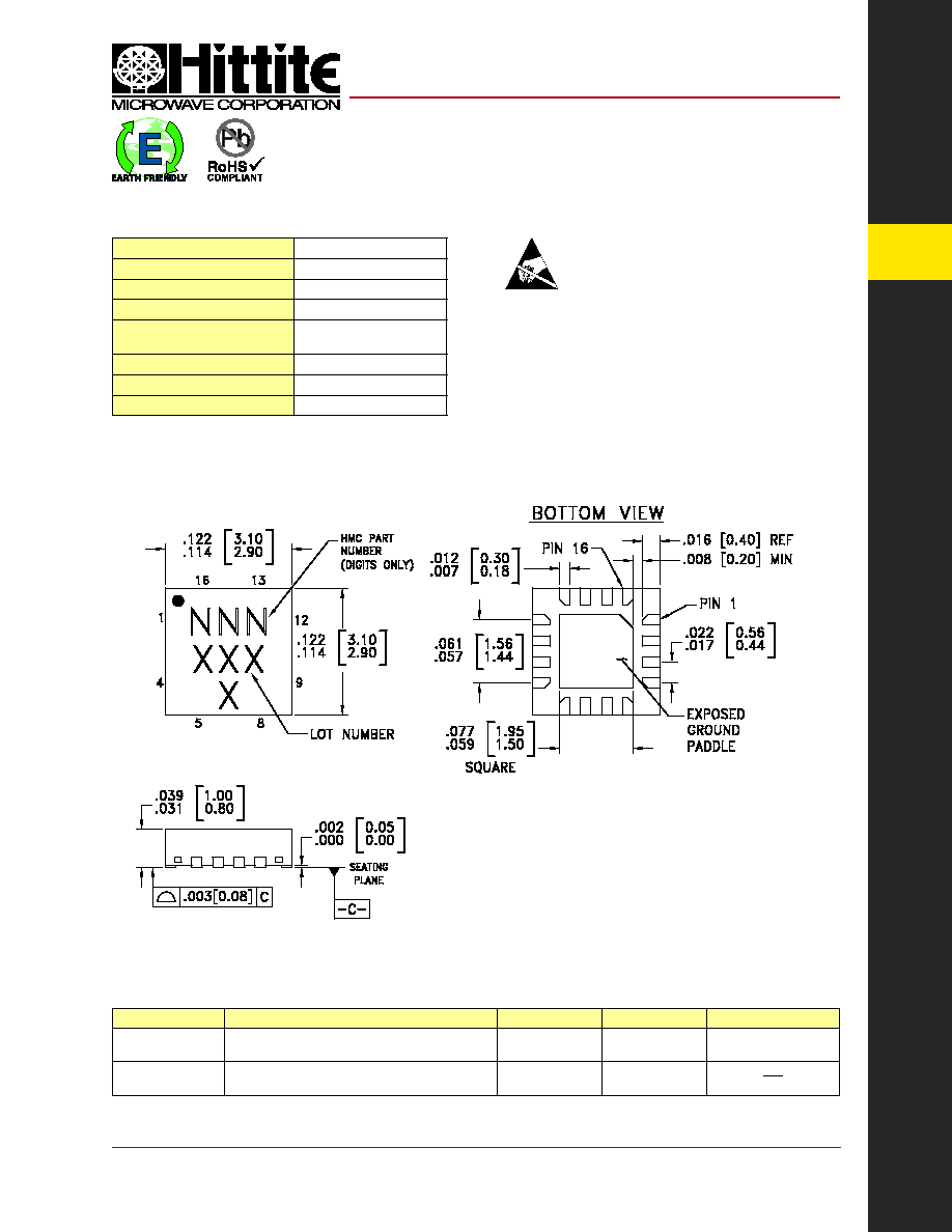
Absolute Maximum Ratings
Outline Drawing
RF Input Power (DC - 5.5 GHz)
+29 dBm (T = +85 °C)
Control Voltage Range (V1 to V4)
-1V to Vdd +1V
Bias Voltage (Vdd)
+7.0 Vdc
Channel Temperature
150 °C
Continuous Pdiss (T = 85 °C)
(derate 11.7 mW/°C above 85 °C)
0.769 W
Thermal Resistance
85 °C/W
Storage Temperature
-65 to +150 °C
Operating Temperature
-40 to +85 °C
NOTES:
1. LEADFRAME MATERIAL: COPPER ALLOY
2. DIMENSIONS ARE IN INCHES [MILLIMETERS]
3. LEAD SPACING TOLERANCE IS NON-CUMULATIVE
4. PAD BURR LENGTH SHALL BE 0.15mm MAXIMUM.
PAD BURR HEIGHT SHALL BE 0.05mm MAXIMUM.
5. PACKAGE WARP SHALL NOT EXCEED 0.05mm.
6. ALL GROUND LEADS AND GROUND PADDLE MUST BE
SOLDERED TO PCB RF GROUND.
7. REFER TO HITTITE APPLICATION NOTE FOR SUGGESTED
LAND PATTERN.
ELECTROSTATIC SENSITIVE DEVICE
OBSERVE HANDLING PRECAUTIONS
HMC540LP3
/
540LP3E
1 dB LSB GaAs MMIC 4-BIT DIGITAL
POSITIVE CONTROL ATTENUATOR, DC - 5.5 GHz
v00.0605
Part Number
Package Body Material
Lead Finish
MSL Rating
Package Marking
[3]
HMC540LP3
Low Stress Injection Molded Plastic
Sn/Pb Solder
MSL1
[1]
540
XXXX
HMC540LP3E
RoHS-compliant Low Stress Injection Molded Plastic
100% matte Sn
MSL1
[2]
540
XXXX
[1] Max peak refl ow temperature of 235 °C
[2] Max peak refl ow temperature of 260 °C
[3] 4-Digit lot number XXXX
Package Information
9
A
T
T
E
N
U
A
T
O
R
S - SM
T
9 - 176
For price, delivery, and to place orders, please contact Hittite Microwave Corporation:
20 Alpha Road, Chelmsford, MA 01824 Phone: 978-250-3343 Fax: 978-250-3373
Order On-line at www.hittite.com
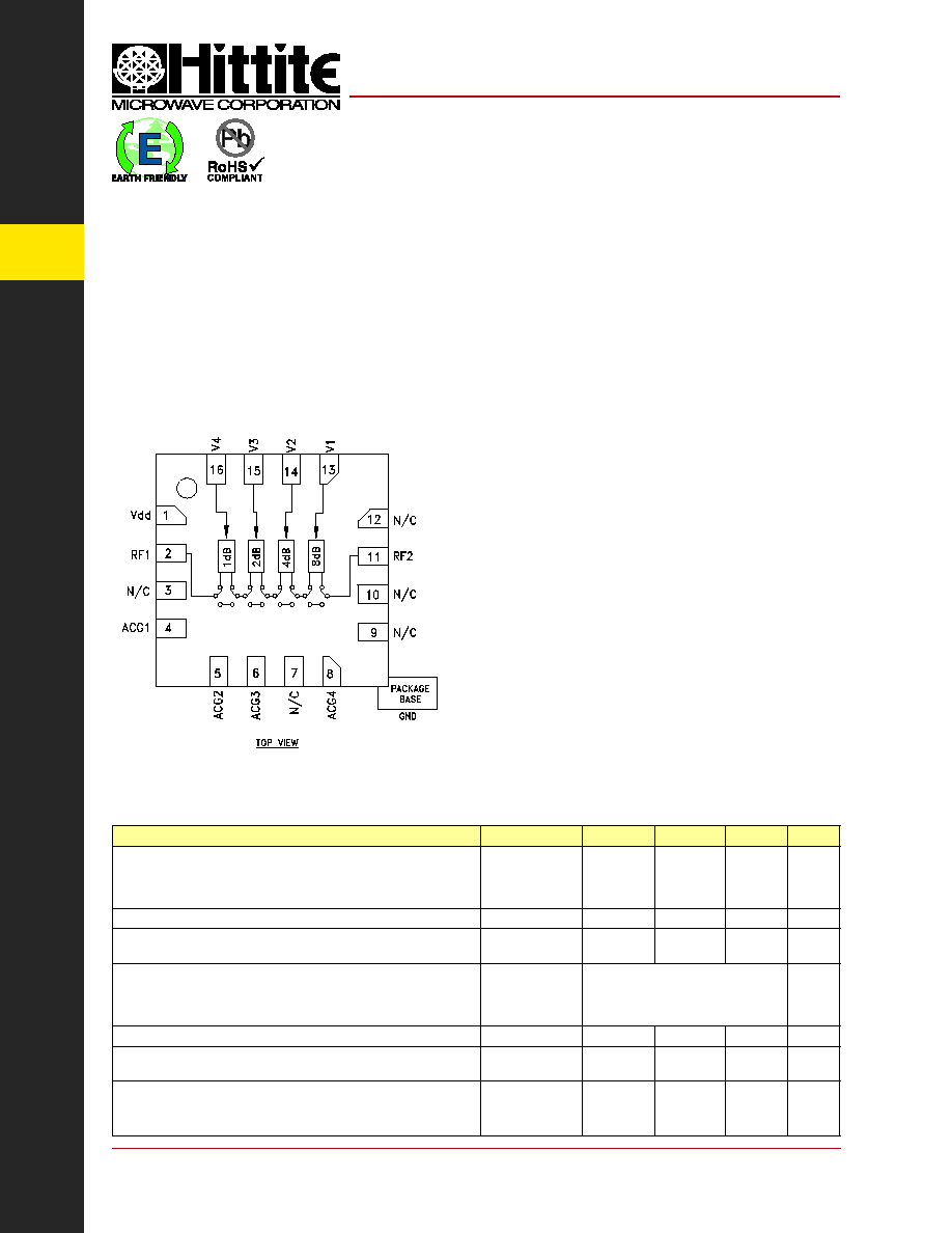
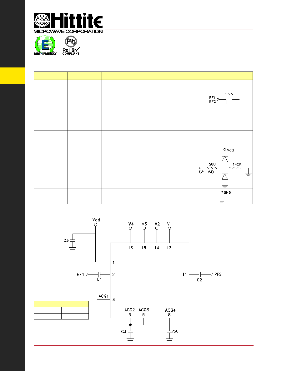
Pin Descriptions
Pin Number
Function
Description
Interface Schematic
1
Vdd
Supply Voltage.
2, 11
RF1, RF2
This pin is DC coupled and matched to 50 Ohm.
Blocking capacitors are required.
Select value based on lowest frequency of operation.
3, 7, 9, 10, 12
N/C
These pins should be connected to PCB RF ground to
maximize performance.
4 - 6, 8
ACG1 - ACG4
External capacitor to ground is required. Select value for
lowest frequency of operation. Place capacitor as close
to pins as possible.
13 - 16
V1 - V4
See truth table and control voltage table.
GND
Package bottom has an exposed metal paddle that must be
connected to RF/DC Ground.
Application Circuit
HMC540LP3
/
540LP3E
1 dB LSB GaAs MMIC 4-BIT DIGITAL
POSITIVE CONTROL ATTENUATOR, DC - 5.5 GHz
v00.0605
Recommended Component Values
C1 - C3
1,000 pF ± 10%
C4, C5
330 pF ± 10%