
MICROWAVE CORPORATION
1 - 30
For price, delivery, and to place orders, please contact Hittite Microwave Corporation:
12 Elizabeth Drive, Chelmsford, MA 01824 Phone: 978-250-3343 Fax: 978-250-3373
Order Online at www.hittite.com
AMPLIFIERS - CHIP
1
HMC392
GaAs MMIC LOW NOISE
AMPLIFIER, 3.5 - 7.0 GHz
v00.1002
General Description
Features
Functional Diagram
The HMC392 is a GaAs MMIC Low Noise
Amplifi er die which operates between 3.5 and 7.0
GHz. The amplifi er provides 15.5 dB of gain, 2.4
dB noise fi gure, and 28 dBm IP3 from a +5.0V
supply voltage. The HMC392 has six bonding
adjustment options which allow the user to select
the bias point and output power of the device (+15
to +18 dBm). The HMC392 amplifi er can easily
be integrated into Multi-Chip-Modules (MCMs)
due to its small (1.3 mm
2
) size. All data is with
the chip in a 50 Ohm test fi xture connected via
0.025mm (1 mil) diameter wire bonds of minimal
length 0.31mm (12 mils).
Gain: 15.5 dB
Noise Figure: 2.4 dB
Single Supply Voltage: +5.0V
50 Ohm Matched Input/Output
No External Components Required
Small Size: 1.3 mm x 1.0 mm x 0.1 mm
Electrical Specifi cations,
T
A
= +25� C, Vdd = 5V
Typical Applications
The HMC392 is ideal for use as a low noise
amplifi er for:
� Point to Point Radios
� VSAT
� LO Driver for HMC Mixers
� Military EW, ECM, C
3
I
� Space
Parameter
Min.
Typ.
Max.
Min.
Typ.
Max.
Units
Frequency Range
4.0 - 6.0
3.5 - 7.0
GHz
Gain
13
15.5
11.5
14
dB
Gain Variation Over Temperature
0.018
0.025
0.018
0.025
dB/ �C
Noise Figure
2.4
3.0
2.8
3.4
dB
Input Return Loss
15
10
dB
Output Return Loss
15
10
dB
Output Power for 1 dB Compression (P1dB)
13
16
12
16
dBm
Saturated Output Power (Psat)
18
18
dBm
Output Third Order Intercept (IP3)
25
28
23
28
dBm
Supply Current (Idd)
50
50
mA
Note: Data taken with pads PS4 and PS8 bonded to ground (state 5) unless otherwise noted.

MICROWAVE CORPORATION
1 - 31
For price, delivery, and to place orders, please contact Hittite Microwave Corporation:
12 Elizabeth Drive, Chelmsford, MA 01824 Phone: 978-250-3343 Fax: 978-250-3373
Order Online at www.hittite.com
AMPLIFIERS - CHIP
1
-25
-20
-15
-10
-5
0
5
10
15
20
2
3
4
5
6
7
8
9
S21
S11
S22
RESPONSE (dB)
FREQUENCY (GHz)
5
6
7
8
9
10
11
12
13
14
15
16
17
18
19
20
3
3.5
4
4.5
5
5.5
6
6.5
7
7.5
8
+25C
+85C
-55C
GAIN (dB)
FREQUENCY (GHz)
-25
-20
-15
-10
-5
0
3
3.5
4
4.5
5
5.5
6
6.5
7
7.5
8
+25C
+85C
-55C
RETURN LOSS (dB)
FREQUENCY (GHz)
-25
-20
-15
-10
-5
0
3
3.5
4
4.5
5
5.5
6
6.5
7
7.5
8
+25C
+85C
-55C
RETURN LOSS (dB)
FREQUENCY (GHz)
GaAs MMIC SUB-HARMONICALLY PUMPED MIXER 17 - 25 GHz
HMC392
Input Return Loss vs. Temperature
Output Return Loss vs. Temperature
GaAs MMIC LOW NOISE
AMPLIFIER, 3.5 - 7.0 GHz
v00.1002
Broadband Gain & Return Loss
Gain vs. Temperature
0
0.5
1
1.5
2
2.5
3
3.5
4
4.5
5
3
3.5
4
4.5
5
5.5
6
6.5
7
7.5
8
+25C
+85C
-55C
NOISE FIGURE (dB)
FREQUENCY (GHz)
Noise Figure vs. Temperature
-60
-50
-40
-30
-20
-10
0
3
3.5
4
4.5
5
5.5
6
6.5
7
7.5
8
+25C
+85C
-55C
ISOLATION (dB)
FREQUENCY (GHz)
Reverse Isolation vs. Temperature

MICROWAVE CORPORATION
1 - 32
For price, delivery, and to place orders, please contact Hittite Microwave Corporation:
12 Elizabeth Drive, Chelmsford, MA 01824 Phone: 978-250-3343 Fax: 978-250-3373
Order Online at www.hittite.com
AMPLIFIERS - CHIP
1
HMC392
v00.1002
20
21
22
23
24
25
26
27
28
29
30
31
32
3
3.5
4
4.5
5
5.5
6
6.5
7
7.5
8
+25C
+85C
-55C
OIP3 (dBm)
FREQUENCY (GHz)
Output IP3 vs. Temperature
Gain, Noise Figure & Power vs.
Supply Voltage @ 5.5 GHz
0
1
2
3
4
5
6
7
8
9
10
11
12
13
14
15
16
17
18
19
20
4.5
4.75
5
5.25
5.5
Gain
Noise Figure
P1dB
Gain (dB), Noise Figure (dB), P1dB (dBm)
Vs (Vdc)
GaAs MMIC LOW NOISE
AMPLIFIER, 3.5 - 7.0 GHz
10
11
12
13
14
15
16
17
18
19
20
21
22
3
3.5
4
4.5
5
5.5
6
6.5
7
7.5
8
+25C
+85C
-55C
P1dB (dBm)
FREQUENCY (GHz)
10
11
12
13
14
15
16
17
18
19
20
21
22
3
3.5
4
4.5
5
5.5
6
6.5
7
7.5
8
+25C
+85C
-55C
Psat (dBm)
FREQUENCY (GHz)
P1dB vs. Temperature
Psat vs. Temperature
10
11
12
13
14
15
16
17
18
19
20
21
22
3.5
4
4.5
5
5.5
6
6.5
State 1 Idd=75mA
State 2 Idd=62mA
State 3 Idd=55mA
State 4 Idd=65mA
State 5 Idd=50mA
State 6 Idd=46mA
P1dB (dBm)
FREQUENCY (GHz)
P1dB vs. Power Select State
Gain & Noise Figure vs.
Power Select State
0
2
4
6
8
10
12
14
16
18
3
3.5
4
4.5
5
5.5
6
6.5
7
7.5
8
Gain State 1
Gain State 2
Gain State 3
Gain State 4
Gain State 5
Gain State 6
NF State 1
NF State 2
NF State 3
NF State 4
NF State 5
NF State 6
GAIN, NOISE FIGURE (dB)
FREQUENCY (GHz)
MICROWAVE CORPORATION
1 - 33
For price, delivery, and to place orders, please contact Hittite Microwave Corporation:
12 Elizabeth Drive, Chelmsford, MA 01824 Phone: 978-250-3343 Fax: 978-250-3373
Order Online at www.hittite.com
AMPLIFIERS - CHIP
1
HMC392
v00.1002
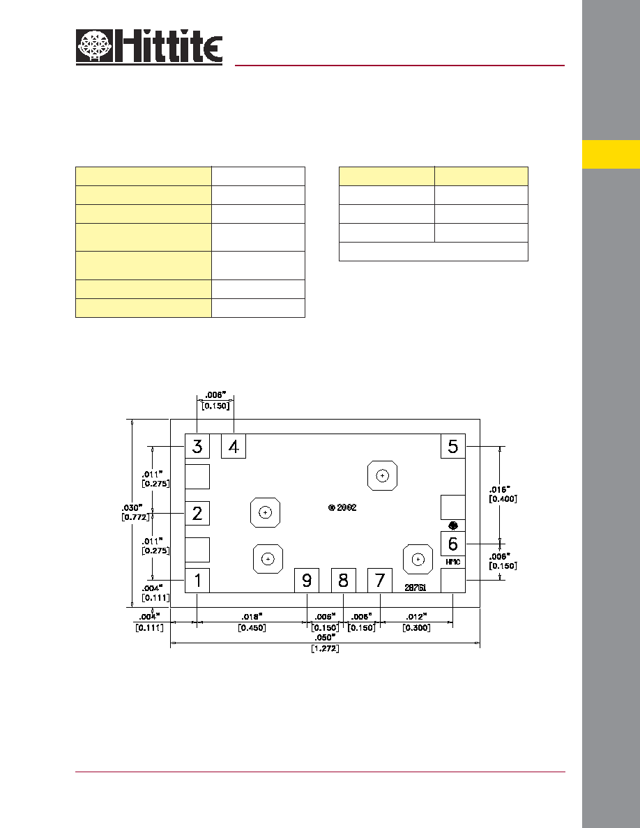
Outline Drawing
Absolute Maximum Ratings
Drain Bias Voltage (Vdd)
+7.0 Vdc
RF Input Power (RFin)(Vdd = +5.0 Vdc)
+15 dBm
Channel Temperature
175 �C
Continuous Pdiss (T= 85 �C)
(derate 8.125 mW/�C above 85 �C)
0.731 W
Thermal Resistance
(channel to die bottom)
123 �C/W
Storage Temperature
-65 to +150 �C
Operating Temperature
-55 to +85� C
NOTES:
1. ALL DIMENSIONS IN INCHES [MILLIMETERS]
2. ALL TOLERANCES ARE �0.001 (0.025)
3. DIE THICKNESS IS 0.004 (0.100) BACKSIDE IS GROUND
4. BOND PADS ARE 0.004 (0.100) SQUARE
5. BOND PAD SPACING, CTR-CTR: 0.006 (0.150)
6. BACKSIDE METALLIZATION: GOLD
7. BOND PAD METALLIZATION: GOLD
GaAs MMIC LOW NOISE
AMPLIFIER, 3.5 - 7.0 GHz
Typical Supply Current vs. Vdd
Vdd (Vdc)
Idd (mA)
+4.5
49
+5.0
50
+5.5
51
(State 5 Depicted)

MICROWAVE CORPORATION
1 - 34
For price, delivery, and to place orders, please contact Hittite Microwave Corporation:
12 Elizabeth Drive, Chelmsford, MA 01824 Phone: 978-250-3343 Fax: 978-250-3373
Order Online at www.hittite.com
AMPLIFIERS - CHIP
1
HMC392
v00.1002
Pad Descriptions
Pad Number
Function
Description
Interface Schematic
2
RF IN
This pad is AC coupled and matched to 50 Ohms
from 3.5 to 7.0 GHz.
3
4
Power Select
PS3
PS4
One of these pads must be connected to ground.
See Power Select Table for selection criteria.
7
8
9
Power Select
PS7
PS8
PS9
One of these pads must be connected to ground.
See Power Select Table for selection criteria.
1, 5
Vdd,
Vdd (alt.)
Power supply voltage. Connect either pad1 or pad5 to +5V
supply. No choke inductor or bypass capacitor is needed.
6
RF OUT
This pad is AC coupled and matched to 50 Ohms
from 3.5 to 7.0 GHz.
Die
Bottom
GND
Die bottom must be connected to RF/DC ground.
Power Select Table
State
Pads Bonded to Ground
Typical Idd (mA)
Typical P1dB (dBm)
1
PS3 & PS7
75
18.4
2
PS3 & PS8
62
17.9
3
PS3 & PS9
55
16.4
4
PS4 & PS7
65
17.7
5
PS4 & PS8
50
16.9
6
PS4 & PS9
46
15.5
GaAs MMIC LOW NOISE
AMPLIFIER, 3.5 - 7.0 GHz