 | ÐлекÑÑоннÑй компоненÑ: SH7604 | СкаÑаÑÑ:  PDF PDF  ZIP ZIP |
Äîêóìåíòàöèÿ è îïèñàíèÿ www.docs.chipfind.ru

SH7604
Hardware Manual
ADE-602-085C
Rev. 4.0
9/19/01
Hitachi, Ltd.

Cautions
1. Hitachi neither warrants nor grants licenses of any rights of Hitachi's or any third party's
patent, copyright, trademark, or other intellectual property rights for information contained in
this document. Hitachi bears no responsibility for problems that may arise with third party's
rights, including intellectual property rights, in connection with use of the information
contained in this document.
2. Products and product specifications may be subject to change without notice. Confirm that you
have received the latest product standards or specifications before final design, purchase or
use.
3. Hitachi makes every attempt to ensure that its products are of high quality and reliability.
However, contact Hitachi's sales office before using the product in an application that
demands especially high quality and reliability or where its failure or malfunction may directly
threaten human life or cause risk of bodily injury, such as aerospace, aeronautics, nuclear
power, combustion control, transportation, traffic, safety equipment or medical equipment for
life support.
4. Design your application so that the product is used within the ranges guaranteed by Hitachi
particularly for maximum rating, operating supply voltage range, heat radiation characteristics,
installation conditions and other characteristics. Hitachi bears no responsibility for failure or
damage when used beyond the guaranteed ranges. Even within the guaranteed ranges,
consider normally foreseeable failure rates or failure modes in semiconductor devices and
employ systemic measures such as fail-safes, so that the equipment incorporating Hitachi
product does not cause bodily injury, fire or other consequential damage due to operation of
the Hitachi product.
5. This product is not designed to be radiation resistant.
6. No one is permitted to reproduce or duplicate, in any form, the whole or part of this document
without written approval from Hitachi.
7. Contact Hitachi's sales office for any questions regarding this document or Hitachi
semiconductor products.

Preface
The SH7604 implements high-performance operations by using a CPU which employs the
Reduced Instruction Set Computer (RISC) system. The SH7604 is a new-generation RISC
microcomputer which realizes low power consumption, an essential feature of microcomputer
devices, as well as integrating peripheral features necessary for system configuration.
The CPU of the SH7604 has a set of RISC-type instructions; basic instructions operate at one state
per instruction, that is, in one system clock cycle, dramatically increasing execution speeds. The
SH7604 incorporates a 32-bit multiplier which performs high-speed sum-of-product (multiply-
and-accumulate) operations. Instructions used by the SH7604 are upwardly compatible with the
SH7000 Series, allowing easy migration from the SH7000 Series to the SH7604.
Moreover, the SH7604 incorporates on-chip peripheral modules such as an interrupt controller
(INTC), direct memory access controller (DMAC), division unit (DIVU), timers (FRT, WDT),
and serial communication interface (SCI), so that a user system can be configured using the
minimum number of parts.
On-chip cache memory enhances the CPU throughput. A bus control feature, which supports
external memory access, improves external memory access efficiency, allowing direct connection
to synchronous DRAM, DRAM, and pseudo-SRAM without the help of glue logic.
This hardware manual explains the hardware features of the SH7604. For details of instructions,
see the Programming Manual.
Related Documents
SH7604 instructions
"SH-1/SH-2 Programming Manual" (Document No.: ADE-602-063B)
For the development environment system, call your nearest Hitachi sales office.


List of Items Revised or Added for This Version
Section
Page
Item
Description
(see Manual for details)
1.1.1 Features of the SH7604
2
Operation Modes
Description of Clock
mode added
4
Package
176-pin plastic TFBGA
(TBP-176) added
1.3.1 Pin Arrangement
5
Product Lineup
Added
8
Figure 1.3 Pin Arrangement
(176-Pin Plastic TFBGA)
Added
1.3.2 Pin Functions
9
Table 1.1 Pin Functions
Pin No. (TBP-176) added
3.2.2 Clock Operating Mode
Setting
51
Description added
52
Table 3.3 Clock Mode Pin
Settings and States
Note 3 added
3.2.7 Notes on Board Design
61
When Using PLL Oscillation
Circuits
Description replaced
62
Figure 3.9 Design Consideration
When Using PLL Oscillation
Circuits
Figure amended,
additional description of
figure
Appendix C
External Dimensions
616
Figure C.2 External Dimensions
(TBP-176)
Added


i
Contents
Section 1
Overview and Pin Functions
........................................................................
1
1.1
SH7604 Features................................................................................................................
1
1.1.1
Features of the SH7604 ........................................................................................
1
1.2
Block Diagram ...................................................................................................................
6
1.3
Description of Pins.............................................................................................................
7
1.3.1
Pin Arrangement ...................................................................................................
7
1.3.2
Pin Functions ........................................................................................................
9
Section 2
CPU
.....................................................................................................................
15
2.1
Register Configuration .......................................................................................................
15
2.1.1
General Registers.................................................................................................. 15
2.1.2
Control Registers .................................................................................................. 16
2.1.3
System Registers...................................................................................................
17
2.1.4
Initial Values of Registers .................................................................................... 17
2.2
Data Formats...................................................................................................................... 18
2.2.1
Data Format in Registers ...................................................................................... 18
2.2.2
Data Format in Memory........................................................................................ 18
2.2.3
Immediate Data Format ........................................................................................ 19
2.3
Instruction Features............................................................................................................ 19
2.3.1
RISC-Type Instruction Set.................................................................................... 19
2.3.2
Addressing Modes ................................................................................................ 22
2.3.3
Instruction Formats ...............................................................................................
25
2.4
Instruction Set .................................................................................................................... 29
2.4.1
Instruction Set by Classification ...........................................................................
29
2.4.2
Operation Code Map.............................................................................................
42
2.5
Processing States................................................................................................................ 44
2.5.1
State Transitions.................................................................................................... 44
2.5.2
Power-Down State ................................................................................................ 46
Section 3
Oscillator Circuits and Operating Modes
................................................ 49
3.1
Overview............................................................................................................................ 49
3.2
On-Chip Clock Pulse Generator and Operating Modes.....................................................
49
3.2.1
Clock Pulse Generator .......................................................................................... 49
3.2.2
Clock Operating Mode Settings............................................................................ 51
3.2.3
Connecting a Crystal Resonator............................................................................ 52
3.2.4
Inputting an External Clock.................................................................................. 54
3.2.5
Selecting Operating Frequency with a Register ...................................................
54
3.2.6
Operating Modes and Frequency Ranges .............................................................
60
3.2.7
Notes on Board Design .........................................................................................
60

ii
3.3
Bus Width of the CS0 Area................................................................................................
62
3.4
Switching between Master Mode and Slave Mode............................................................
63
Section 4
Exception Handling
........................................................................................
65
4.1
Overview............................................................................................................................
65
4.1.1
Types of Exception Handling and Priority Order .................................................
65
4.1.2
Exception Handling Operations............................................................................
66
4.1.3
Exception Vector Table ........................................................................................
67
4.2
Resets .................................................................................................................................
69
4.2.1
Types of Resets .....................................................................................................
69
4.2.2
Power-On Reset ....................................................................................................
70
4.2.3
Manual Reset ........................................................................................................
70
4.3
Address Errors....................................................................................................................
71
4.3.1
Sources of Address Errors ....................................................................................
71
4.3.2
Address Error Exception Handling.......................................................................
72
4.4
Interrupts ............................................................................................................................
72
4.4.1
Interrupt Sources...................................................................................................
72
4.4.2
Interrupt Priority Levels........................................................................................
73
4.4.3
Interrupt Exception Handling ...............................................................................
73
4.5
Exceptions Triggered by Instructions ................................................................................
74
4.5.1
Instruction-Triggered Exception Types ................................................................
74
4.5.2
Trap Instructions ...................................................................................................
74
4.5.3
Illegal Slot Instructions .........................................................................................
74
4.5.4
General Illegal Instructions...................................................................................
75
4.6
When Exception Sources are Not Accepted ......................................................................
75
4.6.1
Immediately after a Delayed Branch Instruction..................................................
75
4.6.2
Immediately after an Interrupt-Disabled Instruction ............................................
76
4.7
Stack Status after Exception Handling ..............................................................................
76
4.8
Usage Notes .......................................................................................................................
76
4.8.1
Value of Stack Pointer (SP) ..................................................................................
76
4.8.2
Value of Vector Base Register (VBR)..................................................................
76
4.8.3
Address Errors Caused by Stacking of Address Error Exception Handling ........
77
4.8.4
Manual Reset during Register Access ..................................................................
77
Section 5
Interrupt Controller (INTC)
.........................................................................
79
5.1
Overview............................................................................................................................
79
5.1.1
Features .................................................................................................................
79
5.1.2
Block Diagram......................................................................................................
79
5.1.3
Pin Configuration..................................................................................................
81
5.1.4
Register Configuration..........................................................................................
81
5.2
Interrupt Sources................................................................................................................
82
5.2.1
NMI Interrupt........................................................................................................
82
5.2.2
User Break Interrupt .............................................................................................
82

iii
5.2.3
IRL Interrupts........................................................................................................
83
5.2.4
On-chip Peripheral Module Interrupts..................................................................
85
5.2.5
Interrupt Exception Vectors and Priority Order....................................................
86
5.3
Description of Registers.....................................................................................................
88
5.3.1
Interrupt Priority Level Setting Register A (IPRA)..............................................
88
5.3.2
Interrupt Priority Level Setting Register B (IPRB) ..............................................
89
5.3.3
Vector Number Setting Register WDT (VCRWDT)............................................
91
5.3.4
Vector Number Setting Register A (VCRA) ........................................................
91
5.3.5
Vector Number Setting Register B (VCRB) ........................................................
92
5.3.6
Vector Number Setting Register C (VCRC) ........................................................
93
5.3.7
Vector Number Setting Register D (VCRD) ........................................................
94
5.3.8
Interrupt Control Register (ICR) ..........................................................................
95
5.4
Interrupt Operation.............................................................................................................
97
5.4.1
Interrupt Sequence ................................................................................................
97
5.4.2
Stack after Interrupt Exception Handling .............................................................
99
5.5
Interrupt Response Time.................................................................................................... 100
5.6
Sampling of Pins
IRL3IRL0 ............................................................................................ 101
5.7
Usage Notes ....................................................................................................................... 103
Section 6
User Break Controller
.................................................................................... 107
6.1
Overview............................................................................................................................ 107
6.1.1
Features ................................................................................................................. 107
6.1.2
Block Diagram...................................................................................................... 108
6.1.3
Register Configuration.......................................................................................... 109
6.2
Register Descriptions ......................................................................................................... 110
6.2.1
Break Address Register A (BARA)...................................................................... 110
6.2.2
Break Address Mask Register A (BAMRA) ........................................................ 111
6.2.3
Break Bus Cycle Register A (BBRA)................................................................... 112
6.2.4
Break Address Register B (BARB) ...................................................................... 114
6.2.5
Break Address Mask Register B (BAMRB)......................................................... 114
6.2.6
Break Data Register B (BDRB)............................................................................ 114
6.2.7
Break Data Mask Register B (BDMRB) .............................................................. 115
6.2.8
Bus Break Register B (BBRB) ............................................................................. 116
6.2.9
Break Control Register (BRCR) ........................................................................... 116
6.3
Operation............................................................................................................................ 120
6.3.1
Flow of the User Break Operation........................................................................ 120
6.3.2
Break on Instruction Fetch Cycle ......................................................................... 120
6.3.3
Break on Data Access Cycle................................................................................. 121
6.3.4
Break on External Bus Cycle................................................................................ 122
6.3.5
Program Counter (PC) Values Saved ................................................................... 122
6.3.6
Example of Use..................................................................................................... 123
6.3.7
Usage Notes .......................................................................................................... 126
6.3.8
SH7000 Series Compatible Mode ........................................................................ 127

iv
Section 7
Bus State Controller (BSC)
.......................................................................... 129
7.1
Overview............................................................................................................................ 129
7.1.1
Features ................................................................................................................. 129
7.1.2
Block Diagram...................................................................................................... 130
7.1.3
Pin Configuration.................................................................................................. 132
7.1.4
Register Configuration.......................................................................................... 134
7.1.5
Address Map ......................................................................................................... 134
7.2
Description of Registers..................................................................................................... 136
7.2.1
Bus Control Register 1 (BCR1)............................................................................ 136
7.2.2
Bus Control Register 2 (BCR2)............................................................................ 138
7.2.3
Wait Control Register (WCR) .............................................................................. 140
7.2.4
Individual Memory Control Register (MCR) ....................................................... 142
7.2.5
Refresh Timer Control/Status Register (RTCSR)................................................. 146
7.2.6
Refresh Timer Counter (RTCNT) ........................................................................ 147
7.2.7
Refresh Time Constant Register (RTCOR) .......................................................... 148
7.3
Access Size and Data Alignment ....................................................................................... 148
7.3.1
Connection to Ordinary Devices .......................................................................... 148
7.3.2
Connection to Little-Endian Devices.................................................................... 150
7.4
Accessing Ordinary Space ................................................................................................. 151
7.4.1
Basic Timing......................................................................................................... 151
7.4.2
Wait State Control ................................................................................................ 155
7.5
Synchronous DRAM Interface .......................................................................................... 157
7.5.1
Synchronous DRAM Direct Connection .............................................................. 157
7.5.2
Address Multiplexing............................................................................................ 159
7.5.3
Burst Reads ........................................................................................................... 160
7.5.4
Single Reads.......................................................................................................... 164
7.5.5
Writes.................................................................................................................... 165
7.5.6
Bank Active Function ........................................................................................... 166
7.5.7
Refreshes............................................................................................................... 174
7.5.8
Power-On Sequence.............................................................................................. 177
7.5.9
Phase Shift by PLL ............................................................................................... 179
7.6
DRAM Interface ................................................................................................................ 181
7.6.1
DRAM Direct Connection .................................................................................... 181
7.6.2
Address Multiplexing............................................................................................ 183
7.6.3
Basic Timing......................................................................................................... 184
7.6.4
Wait State Control ................................................................................................ 185
7.6.5
Burst Access.......................................................................................................... 186
7.6.6
Refresh Timing ..................................................................................................... 188
7.6.7
Power-On Sequence.............................................................................................. 189
7.7
Pseudo-SRAM Interface .................................................................................................... 189
7.7.1
Pseudo-SRAM Direct Connection........................................................................ 189
7.7.2
Basic Timing......................................................................................................... 192
7.7.3
Wait State Control ................................................................................................ 193

v
7.7.4
Burst Access.......................................................................................................... 194
7.7.5
Refreshing ............................................................................................................. 195
7.7.6
Power-On Sequence.............................................................................................. 197
7.8
Burst ROM Interface.......................................................................................................... 197
7.9
Waits between Access Cycles............................................................................................ 200
7.10
Bus Arbitration................................................................................................................... 201
7.10.1 Master Mode ......................................................................................................... 203
7.10.2 Slave Mode ........................................................................................................... 205
7.10.3 Partial-Share Master Mode ................................................................................... 206
7.10.4 External Bus Address Monitor.............................................................................. 209
7.10.5 Master/Slave Coordination ................................................................................... 209
7.11
Other Topics....................................................................................................................... 210
7.11.1 Resets.................................................................................................................... 210
7.11.2 Access as Seen from the CPU or DMAC ............................................................. 210
7.11.3 Emulator................................................................................................................ 212
Section 8
Cache
.................................................................................................................. 213
8.1
Introduction........................................................................................................................ 213
8.2
Cache Control Register (CCR) .......................................................................................... 214
8.3
Address Space and the Cache ............................................................................................ 216
8.4
Cache Operation ................................................................................................................ 216
8.4.1
Cache Reads.......................................................................................................... 216
8.4.2
Write Access ......................................................................................................... 219
8.4.3
Cache-Through Access ......................................................................................... 220
8.4.4
The TAS Instruction ............................................................................................. 221
8.4.5
Pseudo-LRU and Cache Replacement.................................................................. 222
8.4.6
Cache Initialization ............................................................................................... 224
8.4.7
Associative Purges................................................................................................ 224
8.4.8
Data Array Access ................................................................................................ 224
8.4.9
Address Array Access........................................................................................... 225
8.5
Cache Use .......................................................................................................................... 226
8.5.1
Initialization.......................................................................................................... 226
8.5.2
Purge of Specific Lines......................................................................................... 227
8.5.3
Cache Data Coherency.......................................................................................... 227
8.5.4
Two-Way Cache Mode ......................................................................................... 228
8.5.5
Usage Notes .......................................................................................................... 229
Section 9
Direct Memory Access Controller (DMAC)
.......................................... 231
9.1
Overview............................................................................................................................ 231
9.1.1
Features ................................................................................................................. 231
9.1.2
Block Diagram...................................................................................................... 233
9.1.3
Pin Configuration.................................................................................................. 234
9.1.4
Register Configuration.......................................................................................... 234

vi
9.2
Register Descriptions ......................................................................................................... 235
9.2.1
DMA Source Address Registers 0 and 1 (SAR0 and SAR1) ............................... 235
9.2.2
DMA Destination Address Registers 0 and 1 (DAR0 and DAR1) ...................... 236
9.2.3
DMA Transfer Count Registers 0 and 1 (TCR0 and TCR1) ................................ 236
9.2.4
DMA Channel Control Registers 0 and 1 (CHCR0 and CHCR1)........................ 237
9.2.5
DMA Vector Number Registers 0 and 1 (VCRDMA0, VCRDMA1).................. 241
9.2.6
DMA Request/Response Selection Control Registers 0 and 1
(DRCR0, DRCR1)................................................................................................ 242
9.2.7
DMA Operation Register (DMAOR) ................................................................... 243
9.3
Operation............................................................................................................................ 245
9.3.1
DMA Transfer Flow ............................................................................................. 245
9.3.2
DMA Transfer Requests ....................................................................................... 247
9.3.3
Channel Priorities.................................................................................................. 249
9.3.4
DMA Transfer Types............................................................................................ 251
9.3.5
Number of Bus Cycles.......................................................................................... 258
9.3.6
DMA Transfer Request Acknowledge Signal Output Timing ............................. 258
9.3.7
DREQ Pin Input Detection Timing ...................................................................... 268
9.3.8
DMA Transfer End ............................................................................................... 283
9.4
Examples of Use ................................................................................................................ 284
9.4.1
DMA Transfer Between On-Chip SCI and External Memory ............................. 284
9.5
Usage Notes........................................................................................................................ 285
Section 10 Division Unit
.................................................................................................... 287
10.1
Overview............................................................................................................................ 287
10.1.1 Features ................................................................................................................. 287
10.1.2 Block Diagram...................................................................................................... 288
10.1.3 Register Configuration.......................................................................................... 288
10.2
Description of Registers..................................................................................................... 289
10.2.1 Divisor Register (DVSR)...................................................................................... 289
10.2.2 Dividend Register L for 32-Bit Division (DVDNT) ............................................ 289
10.2.3 Division Control Register (DVCR) ...................................................................... 290
10.2.4 Vector Number Setting Register DIV (VCRDIV)................................................ 291
10.2.5 Dividend Register H (DVDNTH)......................................................................... 291
10.2.6 Dividend Register L (DVDNTL).......................................................................... 292
10.3
Operation............................................................................................................................ 292
10.3.1 64-Bit
÷
32-Bit Operations ................................................................................... 292
10.3.2 32-Bit
÷
32-Bit Operations ................................................................................... 292
10.3.3 Handling of Overflows ......................................................................................... 293
10.4
Usage Notes ....................................................................................................................... 293
10.4.1 Access ................................................................................................................... 293
10.4.2 Overflow Flag ....................................................................................................... 294

vii
Section 11 16-Bit Free-Running Timer
......................................................................... 295
11.1
Overview............................................................................................................................ 295
11.1.1 Features ................................................................................................................. 295
11.1.2 Block Diagram...................................................................................................... 296
11.1.3 Pin Configuration.................................................................................................. 297
11.1.4 Register Configuration.......................................................................................... 297
11.2
Register Descriptions ......................................................................................................... 298
11.2.1 Free-Running Counter (FRC) ............................................................................... 298
11.2.2 Output Compare Registers A and B (OCRA and OCRB) .................................... 298
11.2.3 Input Capture Register (ICR)................................................................................ 299
11.2.4 Timer Interrupt Enable Register (TIER)............................................................... 299
11.2.5 Free-Running Timer Control/Status Register (FTCSR) ....................................... 300
11.2.6 Timer Control Register (TCR).............................................................................. 302
11.2.7 Timer Output Compare Control Register (TOCR) ............................................... 303
11.3
CPU Interface..................................................................................................................... 304
11.4
Operation............................................................................................................................ 307
11.4.1 FRC Count Timing ............................................................................................... 307
11.4.2 Output Timing for Output Compare ..................................................................... 308
11.4.3 FRC Clear Timing ................................................................................................ 308
11.4.4 Input Capture Input Timing .................................................................................. 309
11.4.5 Input Capture Flag (ICF) Setting Timing ............................................................. 310
11.4.6 Output Compare Flag (OCFA, OCFB) Setting Timing........................................ 310
11.4.7 Timer Overflow Flag (OVF) Setting Timing ....................................................... 311
11.5
Interrupt Sources................................................................................................................ 312
11.6
Example of FRT Use.......................................................................................................... 312
11.7
Usage Notes ....................................................................................................................... 313
Section 12 Watchdog Timer (WDT)
.............................................................................. 319
12.1
Overview............................................................................................................................ 319
12.1.1 Features ................................................................................................................. 319
12.1.2 Block Diagram...................................................................................................... 320
12.1.3 Pin Configuration.................................................................................................. 320
12.1.4 Register Configuration.......................................................................................... 321
12.2
Register Descriptions ......................................................................................................... 321
12.2.1 Watchdog Timer Counter (WTCNT).................................................................... 321
12.2.2 Watchdog Timer Control/Status Register (WTCSR) ........................................... 322
12.2.3 Reset Control/Status Register (RSTCSR) ............................................................ 323
12.2.4 Register Access..................................................................................................... 324
12.3
Operation............................................................................................................................ 326
12.3.1 Operation in Watchdog Timer Mode.................................................................... 326
12.3.2 Operation in Interval Timer Mode........................................................................ 328
12.3.3 Operation in Standby Mode.................................................................................. 328
12.3.4 Timing of Overflow Flag (OVF) Setting.............................................................. 329

viii
12.3.5 Timing of Watchdog Timer Overflow Flag (WOVF) Setting.............................. 329
12.4
Usage Notes ....................................................................................................................... 330
12.4.1 Contention between WTCNT Write and Increment ............................................. 330
12.4.2 Changing CKS2 to CKS0 Bit Values ................................................................... 330
12.4.3 Switching between Watchdog Timer and Interval Timer Mode .......................... 330
12.4.4 System Reset with
WDTOVF .............................................................................. 331
12.4.5 Internal Reset in Watchdog Timer Mode.............................................................. 331
Section 13 Serial Communication Interface
................................................................. 333
13.1
Overview............................................................................................................................ 333
13.1.1 Features ................................................................................................................. 333
13.1.2 Block Diagram...................................................................................................... 334
13.1.3 Pin Configuration.................................................................................................. 334
13.1.4 Register Configuration.......................................................................................... 335
13.2
Register Descriptions ......................................................................................................... 335
13.2.1 Receive Shift Register (RSR) ............................................................................... 335
13.2.2 Receive Data Register (RDR)............................................................................... 335
13.2.3 Transmit Shift Register (TSR).............................................................................. 336
13.2.4 Transmit Data Register (TDR).............................................................................. 336
13.2.5 Serial Mode Register (SMR) ................................................................................ 336
13.2.6 Serial Control Register (SCR) .............................................................................. 339
13.2.7 Serial Status Register (SSR) ................................................................................. 342
13.2.8 Bit Rate Register (BRR) ....................................................................................... 346
13.3
Operation............................................................................................................................ 352
13.3.1 Overview............................................................................................................... 352
13.3.2 Operation in Asynchronous Mode........................................................................ 354
13.3.3 Multiprocessor Communication............................................................................ 364
13.3.4 Clocked Synchronous Operation .......................................................................... 371
13.4
SCI Interrupt Sources and the DMAC ............................................................................... 381
13.5
Usage Notes ....................................................................................................................... 381
Section 14 Power-Down Modes
...................................................................................... 385
14.1
Overview............................................................................................................................ 385
14.1.1 Power-Down Modes ............................................................................................. 385
14.1.2 Register ................................................................................................................. 386
14.2
Description of Register ...................................................................................................... 387
14.2.1 Standby Control Register (SBYCR) ..................................................................... 387
14.3
Sleep Mode ........................................................................................................................ 389
14.3.1 Transition to Sleep Mode...................................................................................... 389
14.3.2 Canceling Sleep Mode.......................................................................................... 389
14.4
Standby Mode .................................................................................................................... 389
14.4.1 Transition to Standby Mode.................................................................................. 389
14.4.2 Canceling Standby Mode...................................................................................... 390

ix
14.4.3 Standby Mode Cancellation by NMI .................................................................... 391
14.4.4 Clock Pause Function ........................................................................................... 391
14.4.5 Notes on Standby Mode........................................................................................ 393
14.5
Module Standby Function.................................................................................................. 393
14.5.1 Transition to Module Standby Function ............................................................... 393
14.5.2 Clearing the Module Standby Function................................................................ 393
Section 15 Electrical Characteristics (5V Version)
.................................................... 395
15.1
Absolute Maximum Ratings .............................................................................................. 395
15.2
DC Characteristics ............................................................................................................. 396
15.3
AC Characteristics ............................................................................................................. 398
15.3.1 Clock Timing ........................................................................................................ 398
15.3.2 Control Signal Timing .......................................................................................... 402
15.3.3 Bus Timing ........................................................................................................... 408
15.3.4 DMAC Timing...................................................................................................... 474
15.3.5 Free-Running Timer Timing................................................................................. 475
15.3.6 Watchdog Timer Timing ...................................................................................... 476
15.3.7 Serial Communication Interface Timing .............................................................. 477
15.3.8 AC Characteristics Measurement Conditions....................................................... 478
Section 16 Electrical Characteristics (3V Version)
.................................................... 479
16.1
Absolute Maximum Ratings .............................................................................................. 479
16.2
DC Characteristics ............................................................................................................. 480
16.3
AC Characteristics ............................................................................................................. 482
16.3.1 Clock Timing ........................................................................................................ 482
16.3.2 Control Signal Timing .......................................................................................... 486
16.3.3 Bus Timing ........................................................................................................... 492
16.3.4 DMAC Timing...................................................................................................... 558
16.3.5 Free-Running Timer Timing................................................................................. 559
16.3.6 Watchdog Timer Timing ...................................................................................... 560
16.3.7 Serial Communication Interface Timing .............................................................. 561
16.3.8 AC Characteristics Measurement Conditions....................................................... 562
Appendix A Pin States
........................................................................................................ 563
Appendix B List of Registers
........................................................................................... 565
Appendix C External Dimensions
.................................................................................. 615

x

1
Section 1 Overview and Pin Functions
1.1
SH7604 Features
The SH7604 is a new-generation single-chip RISC microprocessor that integrates a Hitachi-
original CPU, a multiplier, cache memory, and peripheral functions required for system
configuration.
The CPU features a RISC-type instruction set
.
Most instructions can be executed in one clock
cycle, which greatly improves instruction execution speed
.
In addition, the on-chip 4-kbyte cache
memory and divider enhance data processing ability.
The SH7604 is also provided with on-chip peripheral functions including a direct memory access
controller (DMAC), timers, a serial communication interface (SCI), and an interrupt controller
.
External memory access support functions (provided by the bus state controller) enable direct
connection to DRAM, synchronous DRAM, and pseudo-SRAM.
The high-speed CPU and comprehensive peripheral functions enable designers to construct high-
performance systems with advanced functionality at low cost, even in applications such as real-
time control that require very high speeds, impossible with conventional microprocessors.
1.1.1
Features of the SH7604
CPU:
·
Original Hitachi architecture
·
32-bit internal configuration
·
General-registers:
Sixteen 32-bit general registers
Three 32-bit control registers
Four 32-bit system registers
·
RISC-type instruction set:
Instruction length: 16-bit fixed length for improved code efficiency
Load-store architecture (basic arithmetic and logic operations are executed between
registers)
Delayed conditional/unconditional branch instructions reduce pipeline disruption during
branching
Instruction set based on C language
·
Instruction execution time: one instruction/state (35 ns/instruction at 28.7 MHz operation)
·
Address space: 4 Gbytes available in the architecture (128-Mbyte memory space)

2
·
On-chip multiplier: multiply operations (32 bits
×
32 bits
64 bits) and multiply-and-
accumulate operations (32 bits
×
32 bits + 64 bits
64 bits) executed in 2 to 4 states
·
Five-stage pipeline
Operating Modes:
·
Clock mode: selected from the combination of an on-chip oscillator module, a frequency
multiplier, clock output, PLL synchronization, and 90
°
phase shifting (the range of choices
depends on the package)
·
Slave/master mode
·
Processing states
Power-on reset state
Manual reset state
Exception handling state
Program execution state
Power-down state
Bus-released state
·
Power-down states
Sleep mode
Standby mode
Module stop mode
Interrupt Controller (INTC):
·
Five external interrupt pins (NMI,
IRL0 to IRL3), encoded input of 15 external interrupt
sources via pins
IRL0 to IRL3
·
Twelve internal interrupt sources (DMAC
×
2, DIVU
×
1, FRT
×
3, WDT
×
1, SCI
×
4,
REF
×
1)
·
Sixteen programmable priority levels
·
Vector number settable for each internal interrupt source
·
Auto-vector or external vector selectable as vector for external interrupts via pins
IRL0 to
IRL3
User Break Controller (UBC):
·
Generates an interrupt when the CPU or DMAC generates an address, data, or bus cycle with
the specified conditions (address, data, CPU cycle/non-CUP cycle, instruction fetch/data
access, read/write, byte/word/longword access)
·
Simplifies configuration of a self-debugger

3
Clock Pulse Generator (CPG)/Phase Locked Loop (PLL):
·
On-chip clock pulse generator
·
Crystal clock source or external clock source can be selected
·
Clock multiplication (
×
1,
×
2,
×
4), PLL synchronization, or 90
°
phase shift can be selected
·
Supports clock pause function for frequency change of external clock
Bus State Controller (BSC):
·
Supports external memory access
32-bit external data bus
·
Memory address space divided into four areas. It is possible to set the following characteristics
for each area (32 Mbyte linear):
Bus size (8, 16, or 32 bits)
Number of wait cycles settable or not settable
Setting the memory space type simplifies connection to DRAM, synchronous DRAM,
pseudo-SRAM, and burst ROM
Outputs signals
RAS, CAS, CE, and OE corresponding to DRAM, synchronous DRAM,
and pseudo-SRAM areas
Tp cycles can be generated to assure RAS precharge time
Address multiplexing is supported internally, so DRAM and synchronous DRAM can be
connected directly
Outputs chip select signals (
CS0 to CS3) for each area
·
DRAM/synchronous DRAM/pseudo-SRAM refresh functions
Programmable refresh interval
Supports CAS-before-RAS refresh and self-refresh modes
·
DRAM/synchronous DRAM/pseudo-SRAM burst access function
Supports high-speed access modes for DRAM/synchronous DRAM/pseudo-SRAM
·
Wait cycles can be inserted by an external WAIT signal
Cache Memory:
·
4 kbytes
·
64 entries, 4-way set associative, 16-byte line length
·
Write-through data writing method
·
LRU replacement algorithm
·
2 kbytes of the cache can be used as 2-kbyte internal RAM

4
Direct Memory Access Controller (DMAC) (2 Channels):
·
Permits DMA transfer between external memory, external I/O, on-chip peripheral modules
·
Enables DMA transfer request and auto-request from external pins, on-chip SCI, and on-chip
timers
·
Cycle-steal mode or burst mode
·
Channel priority level is selectable (fixed mode or round-robin mode)
·
Dual or single address transfer mode is selectable
·
Transfer data width: 1/2/4/16 bytes
·
Address space: 4 Gbytes; maximum number of transfers: 16,777,216
Division Unit (DIVU):
·
Executes 64 ÷ 32
32... 32 and 32 ÷ 32
32... 32 divisions in 39 cycles
·
Overflow interrupt
16-Bit Free-Running Timer (FRT) (1 Channel):
·
Selects input from three internal/external clocks
·
Input capture and output compare
·
Counter overflow, compare match, and input capture interrupts
Watchdog Timer (WDT) (1 Channel):
·
Can be switched between watchdog timer and interval timer functions
·
Count overflow can generate an internal reset, external signal, or interrupt
·
Power-on reset or manual reset can be selected as the internal reset
Serial Communication Interface (SCI) (1 Channel):
·
Asynchronous or synchronous mode is selectable
·
Simultaneous transmission and reception (full duplex)
·
Dedicated baud rate generator
·
Multiprocessor communication function
Package:
·
144-pin plastic QFP (FP-144J)
·
176-pin plastic TFBGA (TBP-176)

5
Product Lineup:
Product Code
Package
Operating Temperature
Frequency
Voltage
HD6417604SF28
QFP2020-144
- 20
°
C to 75
°
C
28 MHz
5 V
HD6417604SFI28
QFP2020-144
- 40
°
C to 85
°
C
28 MHz
5 V
HD6417604SVF20
QFP2020-144
- 20
°
C to 75
°
C
20 MHz
3.3 V
HD6417604SBP28
CSP-1313-176
- 20
°
C to 75
°
C
28 MHz
5 V
HD6417604SVBP20 CSP-1313-176
- 20
°
C to 75
°
C
20 MHz
3.3 V
6
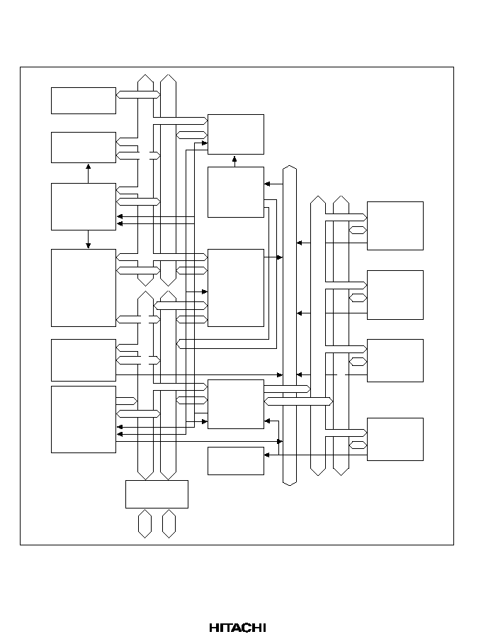
1.2
Block Diagram
Figure 1.1 shows a block diagram of the SH7604.
MULT
Cache
address array
Cache
controller
Cache
data
array
External bus
interface
Clock pulse
generator
Bus state
controller
User break
controller
16-bit free
running
timer
Serial
communi-
cation
interface
Watchdog
timer
Operating-
mode
controller
Exception
handling
interrupt
controller
CPU
DIVU
Direct
memory
access
controller
(
×
2 channels)
Vector address
Peripheral data bus
Peripheral address bus
Internal interrupt signals
Internal address bus
Internal data bus
Cache address bus
Cache data bus
Figure 1.1 Block Diagram
7
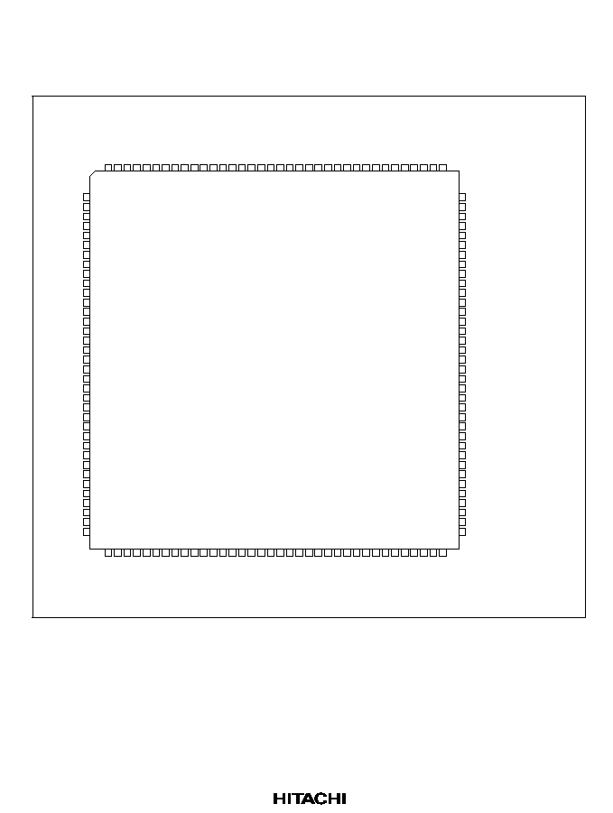
1.3
Description of Pins
1.3.1
Pin Arrangement
1
2
3
4
5
6
7
8
9
10
11
12
13
14
15
16
17
18
19
20
21
22
23
24
25
26
27
28
D11
D12
D13
V
CC
D14
V
SS
D15
D16
D17
D18
D19
D21
D22
D23
V
CC
D24
V
SS
D25
D26
V
CC
D28
V
SS
D29
D30
V
CC
D20
V
SS
D27
29
30
31
32
33
34
35
36
D31
A0
A2
V
SS
A3
A4
A5
A1
CAP1
MD1
V
SS
(PLL)
MD0
V
CC
(PLL)
SCK
TXD
RXD
FTCI
FTI
V
SS
FTOA
V
CC
FTOB
WDTOVF
BREQ
/
BGR
BACK
/
BRLS
V
SS
NC*
WAIT
CKE
RD
V
SS
CASLL
/DQMLL/
WE0
V
CC
CASLH
/DQMLU/
WE1
CASHL
/DQMUL/
WE2
CASHH
/DQMUU/
WE3
108
107
106
105
104
103
102
101
100
99
98
94
93
92
91
90
89
88
87
85
84
83
82
81
97
96
95
86
CAS
/
OE
RAS
/
CE
V
SS
RD/
WR
BS
CS3
CS2
CS1
80
79
77
76
75
74
73
78
37
38
39
40
41
42
43
44
45
46
47
48
49
50
51
52
53
54
55
56
57
58
59
60
61
62
63
64
A6
A7
A8
V
CC
A9
V
SS
A10
A11
A12
A13
A14
A16
A17
A18
V
CC
A19
V
SS
A20
A21
V
CC
A23
V
SS
A24
A25
V
CC
A15
V
SS
A22
65
66
67
68
69
70
71
72
A26
DACK0
DACK1
V
SS
DREQ0
DREQ1
CS0
V
CC
D10
D9
D8
V
SS
D7
V
CC
D6
D5
D4
D3
V
SS
D2
V
CC
D1
D0
IRL0
IRL1
IRL2
IRL3
NMI
IVECF
V
CC
RES
V
SS
MD5
MD4
CKIO
MD3
144
143
142
141
140
139
138
137
136
135
134
130
129
128
127
126
125
124
123
121
120
119
118
117
133
132
131
122
XTAL
V
SS
EXTAL
V
CC
CKPREQ
/CKM
CKRACK
MD2
CAP2
116
115
113
112
111
110
109
114
Top view
(FP-144)
HD6417604
Note: Do not connect anything to the pin abeled NC.
Figure 1.2 Pin Arrangement (144-Pin Plastic QFP)
8
15
14
13
12
11
10
9
8
7
6
5
4
3
2
1
15
14
13
12
11
10
9
8
7
6
5
4
3
2
1
A
B
C
D
E
F
G
H
J
K
L
M
N
P
R
A
B
C
D
E
F
G
H
J
K
L
M
N
P
R
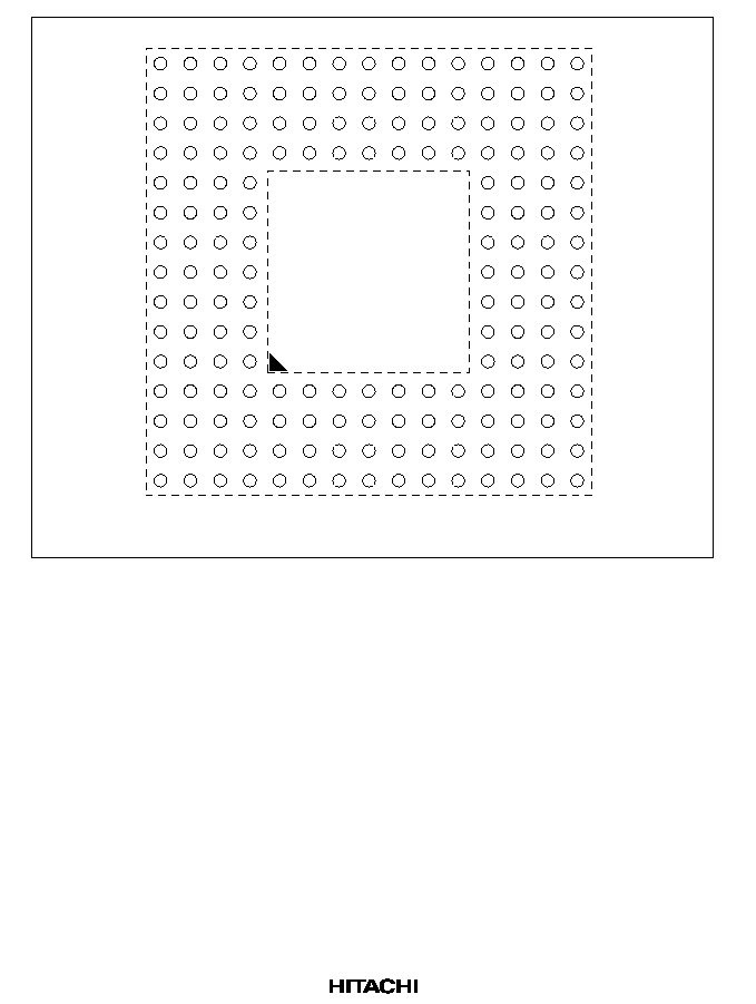
TBP-176
(Top View)
INDEX MARK
Note: The part surrounded by the interrupt line is perspective.
Figure 1.3 Pin Arrangement (176-Pin Plastic TFBGA)

9
1.3.2
Pin Functions
Table 1.2 shows the pin functions of the SH7604.
Table 1.1
Pin Functions
Pin No.
FP-144
TBP-176Pin Name
I/O
Pin Description
--
A1
NC
--
Reserved pin (leave unconnected)
--
C3
NC
--
Reserved pin (leave unconnected)
--
B1
NC
--
Reserved pin (leave unconnected)
--
C2
NC
--
Reserved pin (leave unconnected)
1
D3
D11
I/O
Data bus
2
C1
D12
I/O
Data bus
3
D2
D13
I/O
Data bus
4
E4
V
CC
I
Power
5
D1
D14
I/O
Data bus
6
E3
V
SS
I
Ground
7
E2
D15
I/O
Data bus
8
E1
D16
I/O
Data bus
9
F4
D17
I/O
Data bus
10
F3
D18
I/O
Data bus
11
F1
D19
I/O
Data bus
12
F2
V
CC
I
Power
13
G4
D20
I/O
Data bus
14
G3
V
SS
I
Ground
15
G1
D21
I/O
Data bus
16
G2
D22
I/O
Data bus
17
H4
D23
I/O
Data bus
18
H3
V
CC
I
Power
19
H1
D24
I/O
Data bus
20
H2
V
SS
I
Ground
21
J4
D25
I/O
Data bus
22
J3
D26
I/O
Data bus
23
J1
D27
I/O
Data bus
24
J2
V
CC
I
Power

10
Table 1.1
Pin Functions (cont)
Pin No.
FP-144
TBP-176Pin Name
I/O
Pin Description
25
K4
D28
I/O
Data bus
26
K3
V
SS
I
Ground
27
K1
D29
I/O
Data bus
28
K2
D30
I/O
Data bus
29
L3
D31
I/O
Data bus
30
L1
A0
I/O
Address bus
31
L2
A1
I/O
Address bus
32
L4
A2
I/O
Address bus
33
M1
V
SS
I
Ground
34
M2
A3
I/O
Address bus
35
M3
A4
I/O
Address bus
36
N1
A5
I/O
Address bus
--
M4
NC
--
Reserved pin (leave unconnected)
--
N2
NC
--
Reserved pin (leave unconnected)
--
P1
NC
--
Reserved pin (leave unconnected)
--
P2
NC
--
Reserved pin (leave unconnected)
--
R1
NC
--
Reserved pin (leave unconnected)
--
N3
NC
--
Reserved pin (leave unconnected)
--
R2
NC
--
Reserved pin (leave unconnected)
--
P3
NC
--
Reserved pin (leave unconnected)
37
N4
A6
I/O
Address bus
38
R3
A7
I/O
Address bus
39
P4
A8
I/O
Address bus
40
M5
V
CC
I
Power
41
R4
A9
I/O
Address bus
42
N5
V
SS
I
Ground
43
P5
A10
I/O
Address bus
44
R5
A11
I/O
Address bus
45
M6
A12
I/O
Address bus
46
N6
A13
I/O
Address bus
47
R6
A14
I/O
Address bus

11
Table 1.1
Pin Functions (cont)
Pin No.
FP-144
TBP-176Pin Name
I/O
Pin Description
48
P6
V
CC
I
Power
49
M7
A15
I/O
Address bus
50
N7
V
SS
I
Ground
51
R7
A16
I/O
Address bus
52
P7
A17
I/O
Address bus
53
M8
A18
I/O
Address bus
54
N8
V
CC
I
Power
55
R8
A19
I/O
Address bus
56
P8
V
SS
I
Ground
57
M9
A20
I/O
Address bus
58
N9
A21
I/O
Address bus
59
R9
A22
I/O
Address bus
60
P9
V
CC
I
Power
61
M10
A23
I/O
Address bus
62
N10
V
SS
I
Ground
63
R10
A24
I/O
Address bus
64
P10
A25
I/O
Address bus
65
N11
A26
I/O
Address bus
66
R11
DACK0
O
DMAC0 acknowledge
67
P11
V
CC
I
Power
68
M11
DACK1
O
DMAC1 acknowledge
69
R12
V
SS
I
Ground
70
P12
DREQ0
I
DMAC0 request
71
N12
DREQ1
I
DMAC1 request
72
R13
CS0
O
Chip select 0
--
M12
NC
--
Reserved pin (leave unconnected)
--
P13
NC
--
Reserved pin (leave unconnected)
--
R14
NC
--
Reserved pin (leave unconnected)
--
P14
NC
--
Reserved pin (leave unconnected)
--
R15
NC
--
Reserved pin (leave unconnected)
--
N13
NC
--
Reserved pin (leave unconnected)

12
Table 1.1
Pin Functions (cont)
Pin No.
FP-144
TBP-176Pin Name
I/O
Pin Description
--
P15
NC
--
Reserved pin (leave unconnected)
--
N14
NC
--
Reserved pin (leave unconnected)
73
M13
CS1
O
Chip select 1
74
N15
CS2
O
Chip select 2
75
M14
CS3
O
Chip select 3
76
L12
BS
I/O
Bus cycle start
77
M15
RD/
WR
I/O
Read/write
78
L13
V
SS
I
Ground
79
L14
RAS
/
CE
O
RAS for DRAM and synchronous DRAM, CE
for pseudo-SRAM
80
L15
CAS
/
OE
O
CAS for synchronous DRAM, OE for
pseudo-SRAM
81
K12
CASHH
/DQMUU/
WE3
O
Most significant byte selection signal for
memory
82
K13
CASHL
/DQMUL/
WE2
O
Second byte selection signal for memory
83
K15
CASLH
/DQMLU/
WE1
O
Third byte selection signal for memory
84
K14
V
CC
I
Power
85
J12
CASLL
/DQMLL/
WE0
O
Least significant byte selection signal for
memory
86
J13
V
SS
I
Ground
87
J15
RD
O
Read pulse
88
J14
CKE
O
Synchronous DRAM clock enable control
89
H12
WAIT
I
Hardware wait request
90
H13
NC
--
Reserved pin (leave unconnected)
91
H15
V
SS
I
Ground
92
H14
BACK
/
BRLS
I
Bus acknowledge in slave mode, bus
request in master mode
93
G12
BREQ
/
BGR
O
Bus request in slave mode, bus grant in
master mode
94
G13
WDTOVF
O
Watchdog timer output
95
G15
FTOB
O
Free-running timer output B
96
G14
V
CC
I
Power

13
Table 1.1
Pin Functions (cont)
Pin No.
FP-144
TBP-176Pin Name
I/O
Pin Description
97
F12
FTOA
O
Free-running timer output A
98
F13
V
SS
I
Ground
99
F15
FTI
I
Free-running timer input
100
F14
FTCI
I
Free-running timer clock input
101
E13
RxD
I
Serial data input
102
E15
TxD
O
Serial data output
103
E14
SCK
I/O
Serial clock input/output
104
E12
V
CC
(PLL)
I
Power for on-chip PLL
105
D15
MD0
I
Operating mode pin
106
D14
V
SS
(PLL)
I
Ground for on-chip PLL
107
D13
MD1
I
Operating mode pin
108
C15
CAP1
O
External capacitance pin for PLL
--
D12
NC
--
Reserved pin (leave unconnected)
--
C14
NC
--
Reserved pin (leave unconnected)
--
B15
NC
--
Reserved pin (leave unconnected)
--
B14
NC
--
Reserved pin (leave unconnected)
--
A15
NC
--
Reserved pin (leave unconnected)
--
C13
NC
--
Reserved pin (leave unconnected)
--
A14
NC
--
Reserved pin (leave unconnected)
--
B13
NC
--
Reserved pin (leave unconnected)
109
C12
CAP2
O
External capacitance pin for PLL
110
A13
MD2
I
Operating mode pin
111
B12
CKPACK
O
Clock pause acknowledge output
112
D11
CKPREQ
/CKM
I
Clock pause request input
113
A12
V
CC
I
Power
114
C11
EXTAL
I
Pin for connecting crystal resonator
115
B11
V
SS
I
Ground
116
A11
XTAL
O
Pin for connecting crystal resonator
117
D10
MD3
I
Operating mode pin
118
C10
CKIO
I/O
System clock input/output
119
A10
MD4
I
Operating mode pin

14
Table 1.1
Pin Functions (cont)
Pin No.
FP-144
TBP-176Pin Name
I/O
Pin Description
120
B10
MD5
I
Operating mode pin
121
D9
V
SS
I
Ground
122
C9
RES
I
Reset
123
A9
V
CC
Power
Power
124
B9
IVECF
O
Interrupt vector fetch cycle
125
D8
NMI
I
Nonmaskable interrupt request
126
C8
IRL3
I
External interrupt source input
127
A8
IRL2
I
External interrupt source input
128
B8
IRL1
I
External interrupt source input
129
D7
IRL0
I
External interrupt source input
130
C7
D0
I/O
Data bus
131
A7
D1
I/O
Data bus
132
B7
V
CC
I
Power
133
D6
D2
I/O
Data bus
134
C6
V
SS
I
Ground
135
A6
D3
I/O
Data bus
136
B6
D4
I/O
Data bus
137
C5
D5
I/O
Data bus
138
A5
D6
I/O
Data bus
139
B5
V
CC
I
Power
140
D5
D7
I/O
Data bus
141
A4
V
SS
I
Ground
142
B4
D8
I/O
Data bus
143
C4
D9
I/O
Data bus
144
A3
D10
I/O
Data bus
--
D4
NC
--
Reserved pin (leave unconnected)
--
B3
NC
--
Reserved pin (leave unconnected)
--
A2
NC
--
Reserved pin (leave unconnected)
--
B2
NC
--
Reserved pin (leave unconnected)

15
Section 2 CPU
2.1
Register Configuration
The register set consists of sixteen 32-bit general registers, three 32-bit control registers and four
32-bit system registers.
2.1.1
General Registers
The 16 general registers (R0R15) are shown in figure 2.1. General registers are used for data
processing and address calculation. R0 is also used as an index register, and several instructions
use R0 as a fixed source or destination register. R15 is used as the hardware stack pointer (SP).
Saving and recovering the status register (SR) and program counter (PC) in exception handling is
accomplished by referencing the stack using R15.
R0
R1
R2
R3
R4
R5
R6
R7
R8
R9
R10
R11
R12
R13
R14
R15, SP (hardware stack pointer)
0
31
*
1
*
2
Notes:
1. R0 functions as an index register in the indirect indexed register addressing mode
and indirect indexed GBR addressing mode. In some instructions, R0 functions as a
fixed source register or destination register.
2. R15 functions as a hardware stack pointer (SP) during exception handling.
Figure 2.1 General Registers
16
2.1.2
Control Registers
The 32-bit control registers consist of the 32-bit status register (SR), global base register (GBR),
and vector base register (VBR) (figure 2.2). The status register indicates processing states. The
global base register functions as a base address for the GBR indirect addressing mode to transfer
data to the registers of on-chip peripheral modules. The vector base register functions as the base
address of the exception handling vector area (including interrupts).
9 8 7 6 5 4 3 2 1 0
M Q I3 I2 I1 I0
S T
0
0
31
31
GBR
VBR
SR
31
S bit: Used by the MAC instruction.
Reserved bits. 0 is read, and only 0 must be
written.
Bits I0I3: Interrupt mask bits.
M and Q bits: Used by the DIV0U, DIV0S,
and DIV1 instructions.
Global base register (GBR):
Indicates the base address of the indirect
GBR addressing mode. The indirect GBR
addressing mode is used in data transfer
for on-chip peripheral module register
areas and in logic operations.
Vector base register (VBR):
Indicates the base address of the exception
handling vector area.
SR: Status register
T bit: The MOVT, CMP/cond, TAS, TST,
BT (BT/S), BF (BF/S), SETT, and CLRT
instructions use the T bit to indicate
true (1) or false (0). The ADDV, ADDC,
SUBV, SUBC, DIV0U, DIV0S, DIV1,
NEGC, SHAR, SHAL, SHLR, SHLL,
ROTR, ROTL, ROTCR, and ROTCL
instructions also use the T bit to indicate
carry/borrow or overflow/underflow.
Figure 2.2 Control Registers

17
2.1.3
System Registers
System registers consist of four 32-bit registers: high and low multiply-and-accumulate registers
(MACH and MACL), the procedure register (PR), and the program counter (PC) (figure 2.3). The
multiply-and-accumulate registers store the results of multiply and accumulate operations. The
procedure register stores the return address from the subroutine procedure. The program counter
stores program addresses to control the flow of the processing.
MACL
PR
PC
MACH
31
0
0
0
31
31
Multiply and accumulate (MAC)
registers high and low (MACH,
MACL): Store the results of
multiply-and-accumulate operations.
Procedure register (PR): Stores
a return address from a
subroutine procedure.
Program counter (PC): Indicates
the fourth byte (second instruction)
after the current instruction.
Figure 2.3 System Registers
2.1.4
Initial Values of Registers
Table 2.1 lists the values of the registers after a reset.
Table 2.1
Initial Values of Registers
Classification
Register
Initial Value
General registers
R0R14
Undefined
R15A (SP)
Value of the stack pointer in the vector address table
Control registers
SR
Bits I3I0 are 1111 (H'F), reserved bits are 0, and other
bits are undefined
GBR
Undefined
VBR
H'00000000
System registers
MACH, MACL, PR
Undefined
PC
Value of the program counter in the vector address table
18
2.2
Data Formats
2.2.1
Data Format in Registers
Register operands are always longwords (32 bits) (figure 2.4). When the memory operand is only
a byte (8 bits) or a word (16 bits), it is sign-extended into a longword when loaded into a register.
31
0
Longword
Figure 2.4 Longword Operand
2.2.2
Data Format in Memory
Memory data formats are classified into bytes, words, and longwords. Byte data can be accessed at
any address, but an address error will occur if you try to access word data starting from an address
other than 2n or longword data starting from an address other than 4n. In such cases, the data
accessed cannot be guaranteed (figure 2.5). The hardware stack area, referred to by the hardware
stack pointer (SP, R15), uses only longword data starting from address 4n because this area holds
the program counter and status register.
This microprocessor has a function that allows access of CS2 space (area 2) in little-endian format,
which enables the microprocessor to share memory with processors that access memory in little-
endian format. The microprocessor arranges byte data differently for little-endian and the more
usual big-endian format.
31
0
15
23
7
Byte
Byte
Byte
Byte
Word
Word
Longword
Address 2n
Address 4n
Address m
Address m + 2
Address m + 1
Address m + 3
31
0
15
23
7
Byte
Byte
Byte
Byte
Word
Word
Longword
Big-endian format
Little endian format
Address m + 3
Address m + 1
Address m + 2
Address m
Figure 2.5 Byte, Word, and Longword Alignment

19
2.2.3
Immediate Data Format
Byte (8-bit) immediate data resides in an instruction code. Immediate data accessed by the MOV,
ADD, and CMP/EQ instructions is sign-extended and handled in registers as longword data.
Immediate data accessed by the TST, AND, OR, and XOR instructions is zero-extended and
handled as longword data. Consequently, AND instructions with immediate data always clear the
upper 24 bits of the destination register.
Word or longword immediate data is not located in the instruction code: it is stored in a memory
table. An immediate data transfer instruction (MOV) accesses the memory table using the PC
relative with displacement addressing mode. Specific examples are given in table 2.5, Immediate
Data Accessing.
2.3
Instruction Features
2.3.1
RISC-Type Instruction Set
All instructions are RISC type. This section details their functions.
16-Bit Fixed Length: All instructions are 16 bits long, increasing program code efficiency.
One Instruction per Cycle: The microprocessor can execute basic instructions in one cycle using
the pipeline system. Instructions are executed in 35 ns at 28.7 MHz.
Data Length: Longword is the standard data length for all operations. Memory can be accessed in
bytes, words, or longwords. Byte or word data accessed from memory is sign-extended and
handled as longword data (table 2.2). Immediate data is sign-extended for arithmetic operations or
zero-extended for logic operations. It also is handled as longword data.
Table 2.2
Sign Extension of Word Data
SH7604 CPU
Description
Example of Conventional CPU
MOV.W @(disp,PC),R1
ADD R1,R0
.........
.DATA.W H'1234
Data is sign-extended to 32
bits, and R1 becomes
H'00001234. It is next
operated upon by an ADD
instruction.
ADD.W #H'1234,R0
Note:
@(disp, PC)
accesses the immediate data.
Load-Store Architecture: Basic operations are executed between registers. For operations that
involve memory access, data is loaded into the registers and executed (load-store architecture).
Instructions such as AND that manipulate bits, however, are executed directly in memory.

20
Delayed Branch Instructions: Unconditional branch instructions are delayed. Executing the
instruction that follows the branch instruction, before branching reduces pipeline disruption during
branching (table 2.3).
Table 2.3
Delayed Branch Instructions
SH7604 Series CPU
Description
Example of Conventional CPU
BRA TRGET
ADD R1,R0
Executes ADD before
branching to TRGET
ADD.W R1,R0
BRA TRGET
Multiply and Multiply-and-Accumulate Operations: 16-bit
×
16-bit
32-bit multiply
operations are executed in one to two states. 16-bit
×
16-bit + 64-bit
64-bit multiply-and-
accumulate operations are executed in two to three states. 32-bit
×
32-bit
64-bit multiply and
32-bit
×
32-bit + 64bit
64-bit multiply-and-accumulate operations are executed in two to four
states.
T Bit: The T bit in the status register changes according to the result of the comparison, and in
turn is the condition (true/false) that determines if the program will branch (table 2.4). The number
of instructions that change the T bit is kept to a minimum to improve the processing speed.
Table 2.4
T Bit
SH7604 CPU
Description
Example of Conventional CPU
CMP/GE R1,R0
BT TRGET0
BF TRGET1
T bit is set when R0
R1. The
program branches to TRGET0
when R0
R1 and to TRGET1
when R0 < R1.
CMP.W R1,R0
BGE TRGET0
BLT TRGET1
ADD #1,R0
CMP/EQ #0,R0
BT TRGET
T bit is not changed by ADD.
T bit is set when R0 = 0.
The program branches if R0 = 0.
SUB.W #1,R0
BEQ TRGET
Immediate Data: Byte (8-bit) immediate data resides in the instruction code. Word or longword
immediate data is not input via instruction codes but is stored in a memory table. An immediate
data transfer instruction (MOV) accesses the memory table using the PC relative with
displacement addressing mode (table 2.5).

21
Table 2.5
Immediate Data Accessing
Classification
SH7604 CPU
Example of Conventional CPU
8-bit immediate
MOV #H'12,R0
MOV.B #H'12,R0
16-bit immediate
MOV.W @(disp,PC),R0
.................
.DATA.W H'1234
MOV.W #H'1234,R0
32-bit immediate
MOV.L @(disp,PC),R0
.................
.DATA.L H'12345678
MOV.L #H'12345678,R0
Note:
@(disp, PC)
accesses the immediate data.
Absolute Address: When data is accessed by absolute address, the absolute address value is
placed in the memory table beforehand. Loading the immediate data when the instruction is
executed transfers that value to the register and the data is accessed in the register indirect
addressing mode (table 2.6).
Table 2.6
Absolute Address Accessing
Classification
SH7604 CPU
Example of Conventional CPU
Absolute address
MOV.L @(disp,PC),R1
MOV.B @R1,R0
..................
.DATA.L H'12345678
MOV.B @H'12345678,R0
Note:
@(disp,PC)
accesses the immediate data.
16-Bit/32-Bit Displacement: When data is accessed by 16-bit or 32-bit displacement, the
displacement value is placed in the memory table beforehand. Loading the immediate data when
the instruction is executed transfers that value to the register and the data is accessed in the
indexed register indirect addressing addressing mode (table 2.7).
Table 2.7
16/32-Bit Displacement Accessing
Classification
SH7604 CPU
Example of Conventional CPU
16-bit displacement
MOV.W @(disp,PC),R0
MOV.W @(R0,R1),R2
..................
.DATA.W H'1234
MOV.W @(H'1234,R1),R2
Note:
@(disp,PC)
accesses the immediate data.
22
2.3.2
Addressing Modes
Table 2.8 shows addressing modes and effective address calculation.
Table 2.8
Addressing Modes and Effective Addresses
Addressing
Mode
Instruction
Format
Effective Addresses Calculation
Equation
Register direct
Rn
The effective address is register Rn. (The operand
is the contents of register Rn.)
--
Register
indirect
@Rn
The effective address is the contents of register
Rn.
Rn
Rn
Rn
Register
indirect with
post-increment
@Rn+
The effective address is the contents of register
Rn.
A constant is added to the contents of Rn after the
instruction is executed. 1 is added for a byte
operation, 2 for a word operation, and 4 for a
longword operation.
Rn
Rn
1/2/4
+
Rn + 1/2/4
Rn
(After the
instruction
executes)
Byte: Rn + 1
Rn
Word: Rn + 2
Rn
Longword: Rn
+ 4
Rn
Register
indirect with
pre-decrement
@Rn
The effective address is the value obtained by
subtracting a constant from Rn. 1 is subtracted for
a byte operation, 2 for a word operation, and 4 for
a longword operation.
Rn
1/2/4
Rn 1/2/4
Rn 1/2/4
Byte: Rn 1
Rn
Word: Rn 2
Rn
Longword:
Rn 4
Rn
(Instruction
executed with
Rn after
calculation)
23
Table 2.8
Addressing Modes and Effective Addresses (cont)
Addressing
Mode
Instruction
Format
Effective Addresses Calculation
Equation
Register
indirect with
displacement
@(disp:4,
Rn)
The effective address is Rn plus a 4-bit
displacement (disp). The value of disp is zero-
extended, and remains the same for a byte
operation, is doubled for a word operation, and is
quadrupled for a longword operation.
Rn
Rn + disp
×
1/2/4
+
×
1/2/4
disp
(zero-extended)
Byte: Rn +
disp
Word: Rn +
disp
×
2
Longword:
Rn + disp
×
4
Indexed
register indirect
@(R0, Rn)
The effective address is the Rn value plus R0.
Rn
R0
Rn + R0
+
Rn + R0
GBR indirect
with
displacement
@(disp:8,
GBR)
The effective address is the GBR value plus an
8-bit displacement (disp). The value of disp is
zero-extended, and remains the same for a byte
opera-tion, is doubled for a word operation, and is
quadrupled for a longword operation.
GBR
1/2/4
GBR
+ disp
×
1/2/4
+
×
disp
(zero-extended)
Byte: GBR +
disp
Word: GBR +
disp
×
2
Longword:
GBR + disp
×
4
Indexed GBR
indirect
@(R0,
GBR)
The effective address is the GBR value plus the
R0 value.
GBR
R0
GBR + R0
+
GBR + R0
24
Table 2.8
Addressing Modes and Effective Addresses (cont)
Addressing
Mode
Instruction
Format
Effective Addresses Calculation
Equation
PC relative
with
displacement
@(disp:8,
PC)
The effective address is the PC value plus an 8-bit
displacement (disp). The value of disp is zero-
extended, and remains the same for a byte
operation, is doubled for a word operation, and is
quadrupled for a longword operation. For a
longword operation, the lowest two bits of the PC
value are masked.
PC
H'FFFFFFFC
PC + disp
×
2
or
PC & H'FFFFFFFC
+ disp
×
4
+
2/4
×
&
(for longword operation)
disp
(zero-extended)
Word: PC +
disp
×
2
Longword:
PC &
H'FFFFFFFC
+ disp
×
4
PC relative
disp:8
The effective address is the PC value sign-
extended with an 8-bit displacement (disp),
doubled, and added to the PC value.
PC
2
+
×
disp
(zero-extended)
PC + disp
×
2
PC + disp
×
2
disp:12
The effective address is the PC value sign-
extended with a 12-bit displacement (disp),
doubled, and added to the PC value.
PC
2
+
×
disp
(zero-extended)
PC + disp
×
2
PC + disp
×
2
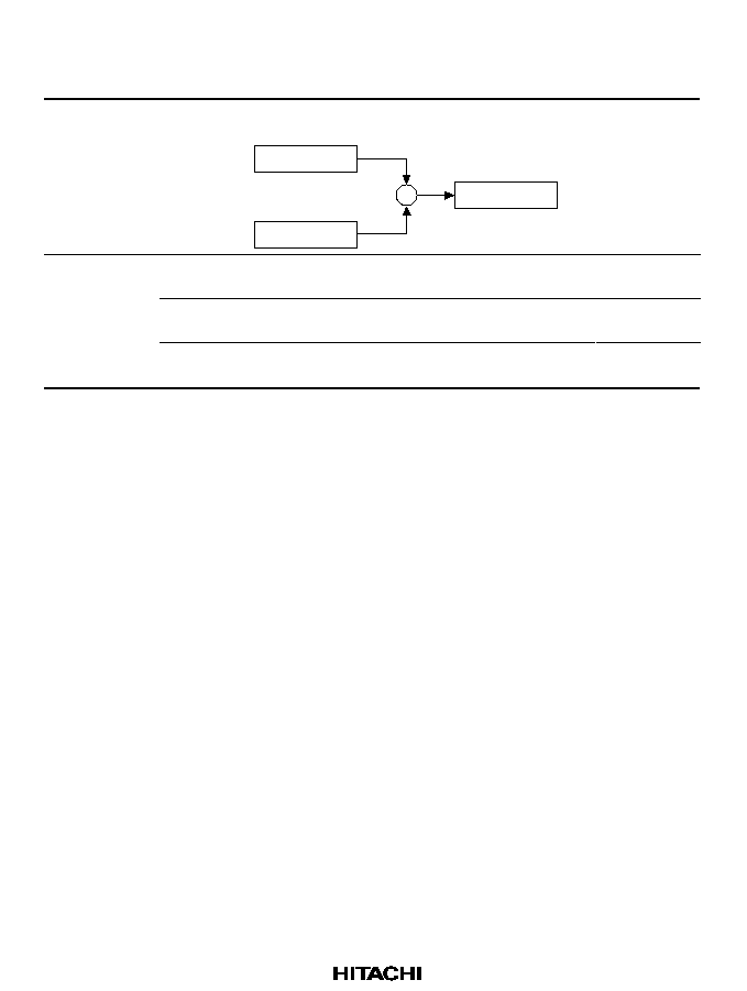
25
Table 2.8
Addressing Modes and Effective Addresses (cont)
Addressing
Mode
Instruction
Format
Effective Addresses Calculation
Equation
PC relative
(cont)
Rn
The effective address is the register PC value
plus Rn.
PC
Rn
PC + Rn
+
PC + Rn
Immediate
#imm:8
The 8-bit immediate data (imm) for the TST,
AND, OR, and XOR instructions is zero-extended.
--
#imm:8
The 8-bit immediate data (imm) for the MOV,
ADD, and CMP/EQ instructions is sign-extended.
--
#imm:8
The 8-bit immediate data (imm) for the TRAPA
instruction is zero-extended and quadrupled.
--
2.3.3
Instruction Formats
Table 2.9 shows instruction formats and source and destination operands. The meaning of the
operands depends on the instruction code. The following symbols are used in the table:
·
xxxx: Instruction code
·
mmmm: Source register
·
nnnn: Destination register
·
iiii: Immediate data
·
dddd: Displacement

26
Table 2.9
Instruction Formats
Instruction Format
Source Operand
Destination
Operand
Example
0 format
xxxx
xxxx
xxxx
xxxx
15
0
--
--
NOP
n format
xxxx
xxxx
xxxx
nnnn
15
0
--
nnnn
: Register
direct
MOVT Rn
Control register or
system register
nnnn
: Register
direct
STS MACH,Rn
Control register or
system register
nnnn
: Register
indirect with
pre-decrement
STC.L SR,@-Rn
m format
xxxx
mmmm
xxxx
xxxx
15
0
mmmm
: Register
direct
Control register or
system register
LDC Rm,SR
mmmm
: Register
indirect with
post-increment
Control register or
system register
LDC.L @Rm+,SR
mmmm
: Register
indirect
--
JMP @Rm
mmmm
: PC relative
using Rm
--
BRAF Rm

27
Table 2.9
Instruction Formats (cont)
Instruction Format
Source Operand
Destination
Operand
Example
nm format
mmmm
: Register
direct
nnnn
: Register
direct
ADD Rm,Rn
nnnn
xxxx
xxxx
15
0
mmmm
mmmm
: Register
direct
nnnn
: Register
indirect
MOV.L Rm,@Rn
mmmm
: Register
indirect with post-
increment (multiply-
and-accumulate)
nnnn
: Register
indirect with post-
increment (multiply-
and-accumulate)*
MACH, MACL
MAC.W
@Rm+,@Rn+
mmmm
: Register
indirect with
post-increment
nnnn
: Register
direct
MOV.L @Rm+,Rn
mmmm
: Register
direct
nnnn
: Register
indirect with
pre-decrement
MOV.L Rm,@-Rn
mmmm
: Register
direct
nnnn
: Indexed
register indirect
MOV.L
Rm,@(R0,Rn)
md format
xxxx
dddd
15
0
mmmm
xxxx
mmmmdddd
:
Register indirect
with displacement
R0 (Register
direct)
MOV.B
@(disp,Rn),R0
nd4 format
xxxx
xxxx
dddd
15
0
nnnn
R0 (Register direct)
nnnndddd
:
Register indirect
with displacement
MOV.B
R0,@(disp,Rn)
nmd format
nnnn
xxxx
dddd
15
0
mmmm
mmmm
: Register
direct
nnnndddd
:
Register indirect
with displacement
MOV.L
Rm,@(disp,Rn)
mmmmdddd
:
Register indirect
with displacement
nnnn
: Register
direct
MOV.L
@(disp,Rm),Rn
28
Table 2.9
Instruction Formats (cont)
Instruction Format
Source Operand
Destination
Operand
Example
d format
dddd
xxxx
15
0
xxxx
dddd
dddddddd
: GBR
indirect with
displacement
R0 (Register
direct)
MOV.L
@(disp,GBR),R0
R0 (Register direct)
dddddddd
: GBR
indirect with
displacement
MOV.L
R0,@(disp,GBR)
dddddddd
: PC
relative with
displacement
R0 (Register
direct)
MOVA
@(disp,PC),R0
dddddddd
: PC
relative
--
BF label
d12 format
dddd
xxxx
15
0
dddd
dddd
dddddddddddd
:
PC relative
--
BRA label
(label = disp + PC)
nd8 format
dddd
nnnn
xxxx
15
0
dddd
dddddddd
: PC
relative with
displacement
nnnn
: Register
direct
MOV.L
@(disp,PC),Rn
i format
iiiiiiii:
Immediate
Indexed GBR
indirect
AND.B
#imm,@(R0,GBR)
xxxx
xxxx
i i i i
15
0
i i i i
iiiiiiii
:
Immediate
R0 (Register
direct)
AND #imm,R0
iiiiiiii:
Immediate
--
TRAPA #imm
ni format
nnnn
i i i i
xxxx
15
0
i i i i
iiiiiiii
:
Immediate
nnnn
: Register
direct
ADD #imm,Rn
Note:
In multiply-and-accumulate instructions,
nnnn
is the source register.

29
2.4
Instruction Set
2.4.1
Instruction Set by Classification
Table 2.10
Instruction Set by Classification
Classification Types
Operation
Code
Function
Number of
Instructions
Data transfer
5
MOV
Data transfer, immediate data transfer,
peripheral module data transfer, structure data
transfer
39
MOVA
Effective address transfer
MOVT
T bit transfer
SWAP
Swap of upper and lower bytes
XTRCT
Extraction of middle of connected registers
Arithmetic
21
ADD
Binary addition
33
operations
ADDC
Binary addition with carry
ADDV
Binary addition with overflow check
CMP/cond Comparison
DIV1
Division
DIV0S
Initialization of signed division
DIV0U
Initialization of unsigned division
DMULS
Signed double-length multiplication
DMULU
Unsigned double-length multiplication
DT
Decrement and test
EXTS
Sign extension
EXTU
Zero extension
MAC
Multiply-and-accumulate, double-length multiply-
and-accumulate operation
MUL
Double-length multiplication
MULS
Signed multiplication
MULU
Unsigned multiplication
NEG
Negation
NEGC
Negation with borrow
SUB
Binary subtraction
SUBC
Binary subtraction with borrow
SUBV
Binary subtraction with underflow check

30
Table 2.10
Instruction Set by Classification (cont)
Classification Types
Operation
Code
Function
Number of
Instructions
Logic
6
AND
Logical AND
14
operations
NOT
Bit inversion
OR
Logical OR
TAS
Memory test and bit set
TST
Logical AND and T bit set
XOR
Exclusive OR
Shift
10
ROTL
One-bit left rotation
14
ROTR
One-bit right rotation
ROTCL
One-bit left rotation with T bit
ROTCR
One-bit right rotation with T bit
SHAL
One-bit arithmetic left shift
SHAR
One-bit arithmetic right shift
SHLL
One-bit logical left shift
SHLLn
n-bit logical left shift
SHLR
One-bit logical right shift
SHLRn
n-bit logical right shift
Branch
9
BF
Conditional branch, conditional branch with
delay (T = 0)
11
BT
Conditional branch, conditional branch with
delay (T = 1)
BRA
Unconditional branch
BRAF
Unconditional branch
BSR
Branch to subroutine procedure
BSRF
Branch to subroutine procedure
JMP
Unconditional branch
JSR
Branch to subroutine procedure
RTS
Return from subroutine procedure

31
Table 2.10
Instruction Set by Classification (cont)
Classification Types
Operation
Code
Function
Number of
Instructions
System
11
CLRT
T bit clear
31
control
CLRMAC
MAC register clear
LDC
Load to control register
LDS
Load to system register
NOP
No operation
RTE
Return from exception handling
SETT
T bit set
SLEEP
Shift to power-down state
STC
Store control register data
STS
Store system register data
TRAPA
Trap exception handling
Total:62
142

32
Table 2.11
Instruction Code Format
Item
Format
Explanation
Instruction
mnemonic
OP.Sz
SRC,DEST
OP: Operation code
Sz: Size (B: byte, W: word, or L: longword)
SRC: Source
DEST: Destination
Rm: Source register
Rn: Destination register
imm: Immediate data
disp: Displacement*
1
Instruction
code
MSB
LSB
mmmm: Source register
nnnn: Destination register
0000: R0
0001: R1
...........
1111: R15
iiii: Immediate data
dddd: Displacement
Operation
,
Direction of transfer
summary
(xx)
Memory operand
M/Q/T
Flag bits in SR
&
Logical AND of each bit
|
Logical OR of each bit
^
Exclusive OR of each bit
~
Logical NOT of each bit
<<n, >>n
n-bit shift
Execution
states
--
Value when no wait states are inserted*
2
T bit
--
Value of T bit after instruction is executed. An em-dash (--)
in the column means no change.
Notes: 1. Depending on the operand size, displacement is scaled
×
1,
×
2, or
×
3. For details, see
the SH-1/SH-2 programming manual.
2. Instruction execution states: The execution states shown in the table are minimums.
The actual number of states may be increased when:
· Contention occurs between instruction fetch and data access
· The destination register of the load instruction (memory
register) and the register
used by the next instruction are the same.

33
Table 2.12
Data Transfer Instructions
Instruction
Instruction Code
Operation
Execu-
tion
States
T
Bit
MOV
#imm,Rn
1110nnnniiiiiiii
#imm
Sign extension
Rn
1
--
MOV.W
@(disp,PC),Rn
1001nnnndddddddd
(disp
×
2 + PC)
Sign
extension
Rn
1
--
MOV.L
@(disp,PC),Rn
1101nnnndddddddd
(disp
×
4 + PC)
Rn
1
--
MOV
Rm,Rn
0110nnnnmmmm0011
Rm
Rn
1
--
MOV.B
Rm,@Rn
0010nnnnmmmm0000
Rm
(Rn)
1
--
MOV.W
Rm,@Rn
0010nnnnmmmm0001
Rm
(Rn)
1
--
MOV.L
Rm,@Rn
0010nnnnmmmm0010
Rm
(Rn)
1
--
MOV.B
@Rm,Rn
0110nnnnmmmm0000
(Rm)
Sign extension
Rn
1
--
MOV.W
@Rm,Rn
0110nnnnmmmm0001
(Rm)
Sign extension
Rn
1
--
MOV.L
@Rm,Rn
0110nnnnmmmm0010
(Rm)
Rn
1
--
MOV.B
Rm,@Rn
0010nnnnmmmm0100
Rn1
Rn, Rm
(Rn)
1
--
MOV.W
Rm,@Rn
0010nnnnmmmm0101
Rn2
Rn, Rm
(Rn)
1
--
MOV.L
Rm,@Rn
0010nnnnmmmm0110
Rn4
Rn, Rm
(Rn)
1
--
MOV.B
@Rm+,Rn
0110nnnnmmmm0100
(Rm)
Sign extension
Rn,Rm + 1
Rm
1
--
MOV.W
@Rm+,Rn
0110nnnnmmmm0101
(Rm)
Sign extension
Rn,Rm + 2
Rm
1
--
MOV.L
@Rm+,Rn
0110nnnnmmmm0110
(Rm)
Rn,Rm + 4
Rm
1
--
MOV.B
R0,@(disp,Rn)
10000000nnnndddd
R0
(disp + Rn)
1
--
MOV.W
R0,@(disp,Rn)
10000001nnnndddd
R0
(disp
×
2 + Rn)
1
--
MOV.L
Rm,@(disp,Rn)
0001nnnnmmmmdddd
Rm
(disp
×
4 + Rn)
1
--
MOV.B
@(disp,Rm),R0
10000100mmmmdddd
(disp + Rm)
Sign
extension
R0
1
--
MOV.W
@(disp,Rm),R0
10000101mmmmdddd
(disp
×
2 + Rm)
Sign
extension
R0
1
--
MOV.L
@(disp,Rm),Rn
0101nnnnmmmmdddd
(disp
×
4 + Rm)
Rn
1
--
MOV.B
Rm,@(R0,Rn)
0000nnnnmmmm0100
Rm
(R0 + Rn)
1
--
MOV.W
Rm,@(R0,Rn)
0000nnnnmmmm0101
Rm
(R0 + Rn)
1
--
MOV.L
Rm,@(R0,Rn)
0000nnnnmmmm0110
Rm
(R0 + Rn)
1
--

34
Table 2.12
Data Transfer Instructions (cont)
Instruction
Instruction Code
Operation
Execu-
tion
States
T
Bit
MOV.B
@(R0,Rm),Rn
0000nnnnmmmm1100
(R0 + Rm)
Sign
extension
Rn
1
--
MOV.W
@(R0,Rm),Rn
0000nnnnmmmm1101
(R0 + Rm)
Sign
extension
Rn
1
--
MOV.L
@(R0,Rm),Rn
0000nnnnmmmm1110
(R0 + Rm)
Rn
1
--
MOV.B
R0,@(disp,GBR)
11000000dddddddd
R0
(disp + GBR)
1
--
MOV.W
R0,@(disp,GBR)
11000001dddddddd
R0
(disp
×
2 + GBR)
1
--
MOV.L
R0,@(disp,GBR)
11000010dddddddd
R0
(disp
×
4 + GBR)
1
--
MOV.B
@(disp,GBR),R0
11000100dddddddd
(disp + GBR)
Sign
extension
R0
1
--
MOV.W
@(disp,GBR),R0
11000101dddddddd
(disp
×
2 + GBR)
Sign
extension
R0
1
--
MOV.L
@(disp,GBR),R0
11000110dddddddd
(disp
×
4 + GBR)
R0
1
--
MOVA
@(disp,PC),R0
11000111dddddddd
disp
×
4 + PC
R0
1
--
MOVT
Rn
0000nnnn00101001
T
Rn
1
--
SWAP.B Rm,Rn
0110nnnnmmmm1000
Rm
Swap the bottom
two bytes
Rn
1
--
SWAP.W Rm,Rn
0110nnnnmmmm1001
Rm
Swap two
consecutive words
Rn
1
--
XTRCT
Rm,Rn
0010nnnnmmmm1101
Rm: Middle 32 bits of
Rn
Rn
1
--

35
Table 2.13
Arithmetic Instructions
Instruction
Instruction Code
Operation
Execution
States
T Bit
ADD
Rm,Rn
0011nnnnmmmm1100
Rn + Rm
Rn
1
--
ADD
#imm,Rn
0111nnnniiiiiiii
Rn + imm
Rn
1
--
ADDC
Rm,Rn
0011nnnnmmmm1110
Rn + Rm + T
Rn,
Carry
T
1
Carry
ADDV
Rm,Rn
0011nnnnmmmm1111
Rn + Rm
Rn,
Overflow
T
1
Overflow
CMP/EQ
#imm,R0
10001000iiiiiiii
If R0 = imm, 1
T
1
Comparison
result
CMP/EQ
Rm,Rn
0011nnnnmmmm0000
If Rn = Rm, 1
T
1
Comparison
result
CMP/HS
Rm,Rn
0011nnnnmmmm0010
If Rn
Rm with
unsigned data, 1
T
1
Comparison
result
CMP/GE
Rm,Rn
0011nnnnmmmm0011
If Rn
Rm with
signed data, 1
T
1
Comparison
result
CMP/HI
Rm,Rn
0011nnnnmmmm0110
If Rn > Rm with
unsigned data, 1
T
1
Comparison
result
CMP/GT
Rm,Rn
0011nnnnmmmm0111
If Rn > Rm with
signed data, 1
T
1
Comparison
result
CMP/PZ
Rn
0100nnnn00010001
If Rn
0, 1
T
1
Comparison
result
CMP/PL
Rn
0100nnnn00010101
If Rn > 0, 1
T
1
Comparison
result
CMP/ST
Rm,Rn
0010nnnnmmmm1100
If Rn and Rm have
an equivalent byte,
1
T
1
Comparison
result
DIV1
Rm,Rn
0011nnnnmmmm0100
Single-step division
(Rn
÷
Rm)
1
Calculation
result
DIV0S
Rm,Rn
0010nnnnmmmm0111
MSB of Rn
Q,
MSB of Rm
M,
M ^ Q
T
1
Calculation
result
DIV0U
0000000000011001
0
M/Q/T
1
0
DMULS.
Rm,Rn
0011nnnnmmmm1101
Signed operation of
Rn
×
Rm
MACH,
MACL 32
×
32
64
bits
2 to 4
*
--

36
Table 2.13
Arithmetic Instructions (cont)
Instruction
Instruction Code
Operation
Execution
States
T Bit
DMULU.L Rm,Rn
0011nnnnmmmm0101
Unsigned operation
of Rn
×
Rm
MACH, MACL 32
×
32
64 bit
2 to 4
*
--
DT
Rn
0100nnnn00010000
Rn 1
Rn, when
Rn is 0, 1
T
When Rn is nonzero,
0
T
1
Comparison
result
EXTS.B
Rm,Rn
0110nnnnmmmm1110
A byte in Rm is sign-
extended
Rn
1
--
EXTS.W
Rm,Rn
0110nnnnmmmm1111
A word in Rm is sign-
extended
Rn
1
--
EXTU.B
Rm,Rn
0110nnnnmmmm1100
A byte in Rm is zero-
extended
Rn
1
--
EXTU.W
Rm,Rn
0110nnnnmmmm1101
A word in Rm is zero-
extended
Rn
1
--
MAC.L
@Rm+,@Rn+
0000nnnnmmmm1111
Signed operation of
(Rn)
×
(Rm)
MAC
MAC 32
×
32
64 bits
3/(2 to 4)
*
--
MAC
@Rm+,@Rn+
0100nnnnmmmm1111
Signed operation of
(Rn)
×
(Rm) + MAC
MAC 16
×
16 + 64
64 bits
3/(2)
*
--
MUL.L
Rm,Rn
0000nnnnmmmm0111
Rn
×
Rm
MACL,
32
×
32
32 bits
2 to 4
*
--
MULS.W
Rm,Rn
0010nnnnmmmm1111
Signed operation of
Rn
×
Rm
MAC 16
×
16
32 bits
1 to 3
*
--
MULU.W
Rm,Rn
0010nnnnmmmm1110
Unsigned operation
of Rn
×
Rm
MAC
16
×
16
32 bits
1 to 3
*
--
NEG
Rm,Rn
0110nnnnmmmm1011
0Rm
Rn
1
--
NEGC
Rm,Rn
0110nnnnmmmm1010
0RmT
Rn,
Borrow
T
1
Borrow

37
Table 2.13
Arithmetic Instructions (cont)
Instruction
Instruction Code
Operation
Execution
States
T Bit
SUB
Rm,Rn
0011nnnnmmmm1000
RnRm
Rn
1
--
SUBC
Rm,Rn
0011nnnnmmmm1010
RnRmT
Rn,
Borrow
T
1
Borrow
SUBV
Rm,Rn
0011nnnnmmmm1011
RnRm
Rn,
Underflow
T
1
Underflow
Note:
The normal minimum number of execution cycles. (The number in parentheses is the
number of cycles when there is contention with preceding or following instructions.)
Table 2.14
Logic Operation Instructions
Instruction
Instruction Code
Operation
Execu-
tion
States
T Bit
AND
Rm,Rn
0010nnnnmmmm1001
Rn & Rm
Rn
1
--
AND
#imm,R0
11001001iiiiiiii
R0 & imm
R0
1
--
AND.B
#imm,@(R0,GBR)
11001101iiiiiiii
(R0 + GBR) & imm
(R0 + GBR)
3
--
NOT
Rm,Rn
0110nnnnmmmm0111
~Rm
Rn
1
--
OR
Rm,Rn
0010nnnnmmmm1011
Rn | Rm
Rn
1
--
OR
#imm,R0
11001011iiiiiiii
R0 | imm
R0
1
--
OR.B
#imm,@(R0,GBR)
11001111iiiiiiii
(R0 + GBR) | imm
(R0 + GBR)
3
--
TAS.B
@Rn
0100nnnn00011011
If (Rn) is 0, 1
T; 1
MSB of (Rn)
4
Test
result
TST
Rm,Rn
0010nnnnmmmm1000
Rn & Rm; if the result is
0, 1
T
1
Test
result
TST
#imm,R0
11001000iiiiiiii
R0 & imm; if the result is
0, 1
T
1
Test
result
TST.B
#imm,@(R0,GBR)
11001100iiiiiiii
(R0 + GBR) & imm; if the
result is 0, 1
T
3
Test
result
XOR
Rm,Rn
0010nnnnmmmm1010
Rn ^ Rm
Rn
1
--
XOR
#imm,R0
11001010iiiiiiii
R0 ^ imm
R0
1
--
XOR.B
#imm,@(R0,GBR)
11001110iiiiiiii
(R0 + GBR) ^ imm
(R0 + GBR)
3
--

38
Table 2.15
Shift Instructions
Instruction
Instruction Code
Operation
Execution
States
T Bit
ROTL
Rn
0100nnnn00000100
T
Rn
MSB
1
MSB
ROTR
Rn
0100nnnn00000101
LSB
Rn
T
1
LSB
ROTCL
Rn
0100nnnn00100100
T
Rn
T
1
MSB
ROTCR
Rn
0100nnnn00100101
T
Rn
T
1
LSB
SHAL
Rn
0100nnnn00100000
T
Rn
0
1
MSB
SHAR
Rn
0100nnnn00100001
MSB
Rn
T
1
LSB
SHLL
Rn
0100nnnn00000000
T
Rn
0
1
MSB
SHLR
Rn
0100nnnn00000001
0
Rn
T
1
LSB
SHLL2
Rn
0100nnnn00001000
Rn<<2
Rn
1
--
SHLR2
Rn
0100nnnn00001001
Rn>>2
Rn
1
--
SHLL8
Rn
0100nnnn00011000
Rn<<8
Rn
1
--
SHLR8
Rn
0100nnnn00011001
Rn>>8
Rn
1
--
SHLL16 Rn
0100nnnn00101000
Rn<<16
Rn
1
--
SHLR16 Rn
0100nnnn00101001
Rn>>16
Rn
1
--

39
Table 2.16
Branch Instructions
Instruction
Instruction Code
Operation
Execution
States
T
Bit
BF
label
10001011dddddddd
If T = 0, disp
×
2 + PC
PC; if T =
1, nop
3/1
*
--
BF/S
label
10001111dddddddd
Delayed branch, if T = 0, disp
×
2 +
PC
PC; if T = 1, nop
2/1
*
--
BT
label
10001001dddddddd
Delayed branch, if T = 1, disp
×
2 +
PC
PC; if T = 0, nop
3/1
*
--
BT/S
label
10001101dddddddd
If T = 1, disp
×
2 + PC
PC; if T =
0, nop
2/1
*
--
BRA
label
1010dddddddddddd
Delayed branch, disp
×
2 + PC
PC
2
--
BRAF
Rm
0000mmmm00100011
Delayed branch, Rm + PC
PC
2
--
BSR
label
1011dddddddddddd
Delayed branch, PC
PR, disp
×
2 + PC
PC
2
--
BSRF
Rm
0000mmmm00000011
Delayed branch, PC
PR,
Rm + PC
PC
2
--
JMP
@Rm
0100mmmm00101011
Delayed branch, Rm
PC
2
--
JSR
@Rm
0100mmmm00001011
Delayed branch, PC
PR,
Rm
PC
2
--
RTS
0000000000001011
Delayed branch, PR
PC
2
--
Note:
One state when the instruction does not branch.

40
Table 2.17
System Control Instructions
Instruction
Instruction Code
Operation
Execu-
tion
States
T
Bit
CLRT
0000000000001000
0
T
1
0
CLRMAC
0000000000101000
0
MACH, MACL
1
--
LDC
Rm,SR
0100mmmm00001110
Rm
SR
1
LSB
LDC
Rm,GBR
0100mmmm00011110
Rm
GBR
1
--
LDC
Rm,VBR
0100mmmm00101110
Rm
VBR
1
--
LDC.L
@Rm+,SR
0100mmmm00000111
(Rm)
SR, Rm + 4
Rm
3
LSB
LDC.L
@Rm+,GBR
0100mmmm00010111
(Rm)
GBR, Rm + 4
Rm
3
--
LDC.L
@Rm+,VBR
0100mmmm00100111
(Rm)
VBR, Rm + 4
Rm
3
--
LDS
Rm,MACH
0100mmmm00001010
Rm
MACH
1
--
LDS
Rm,MACL
0100mmmm00011010
Rm
MACL
1
--
LDS
Rm,PR
0100mmmm00101010
Rm
PR
1
--
LDS.L
@Rm+,MACH
0100mmmm00000110
(Rm)
MACH, Rm + 4
Rm
1
--
LDS.L
@Rm+,MACL
0100mmmm00010110
(Rm)
MACL, Rm + 4
Rm
1
--
LDS.L
@Rm+,PR
0100mmmm00100110
(Rm)
PR, Rm + 4
Rm
1
--
NOP
0000000000001001
No operation
1
--
RTE
0000000000101011
Delayed branch, stack area
PC/SR
4
--
SETT
0000000000011000
1
T
1
1
SLEEP
0000000000011011
Sleep
3
*
--
STC
SR,Rn
0000nnnn00000010
SR
Rn
1
--
STC
GBR,Rn
0000nnnn00010010
GBR
Rn
1
--
STC
VBR,Rn
0000nnnn00100010
VBR
Rn
1
--
STC.L
SR,@Rn
0100nnnn00000011
Rn4
Rn, SR
(Rn)
2
--
STC.L
GBR,@Rn
0100nnnn00010011
Rn4
Rn, GBR
(Rn)
2
--
STC.L
VBR,@Rn
0100nnnn00100011
Rn4
Rn, VBR
(Rn)
2
--

41
Table 2.17
System Control Instructions (cont)
Instruction
Instruction Code
Operation
Execu-
tion
States
T
Bit
STS
MACH,Rn
0000nnnn00001010
MACH
Rn
1
--
STS
MACL,Rn
0000nnnn00011010
MACL
Rn
1
--
STS
PR,Rn
0000nnnn00101010
PR
Rn
1
--
STS.L
MACH,@Rn
0100nnnn00000010
Rn4
Rn, MACH
(Rn)
1
--
STS.L
MACL,@Rn
0100nnnn00010010
Rn4
Rn, MACL
(Rn)
1
--
STS.L
PR,@Rn
0100nnnn00100010
Rn4
Rn, PR
(Rn)
1
--
TRAPA
#imm
11000011iiiiiiii
PC/SR
stack area, (imm)
PC
8
--
Note:
The number of execution states before the chip enters the sleep mode.
Instruction states: The values shown for the execution states are minimums. The actual
number of states may be increased when:
·
Contention occurs between instruction fetch and data access
·
The destination register of the load instruction (memory
register) and the register used
by the next instruction are the same.

42
2.4.2
Operation Code Map
Table 2.18
Operation Code Map
Instruction Code
Fx: 0000
Fx: 0001
Fx: 0010
Fx: 00111111
MSB LSB
MD: 00
MD: 01
MD: 10
MD: 11
0000 Rn
Fx
0000
0000 Rn
Fx
0001
0000 Rn
Fx
0010
STC SR,Rn
STC GBR,Rn
STC VBR,Rn
0000 Rm
Fx
0011
BSRF Rm
BRAF Rm
0000 Rn
Rm 01MD
MOV.B RM,
@(R0,Rn)
MOV.W RM,
@(R0,Rn)
MOV.L RM,
@(R0,Rn)
MUL.L Rm,Rn
0000 0000 Fx
1000
CLRT
SETT
CLRMAC
0000 0000 Fx
1001
NOP
DIVOU
0000 0000 Fx
1010
0000 0000 Fx
1011
RTS
SLEEP
RTE
0000 Rn
Fx
1000
0000 Rn
Fx
1001
MOVT Rn
0000 Rn
Fx
1010
STS MACH,Rn
STS MACL,Rn
STS PR,Rn
0000 Rn
Fx
1011
0000 Rn
Rm 11MD
MOV.B
@(R0,Rm),Rn
MOV.W
@(R0,Rm),Rn
MOV.L
@(R0,Rm),Rn
MAC.L
@Rm+,@Rn+
0001 Rn
Rm disp
MOV.L Rm,@(disp:4,Rn)
0010 Rn
Rm 00MD
MOV.B Rm,@Rn
MOV.W Rm,@Rn
MOV.L Rm,@Rn
0010 Rn
Rm 01MD
MOV.B Rm,
@-Rn
MOV.W Rm,
@Rn
MOV.L Rm,
@Rn
DIV0S Rm,Rn
0010 Rn
Rm 10MD
TST Rm,Rn
AND Rm,Rn
XOR Rm,Rn
OR Rm,Rn
0010 Rn
Rm 11MD
CMP/STR
Rm,Rn
XTRCT
Rm,Rn
MULU.W Rm,Rn
MULS.W Rm,Rn
0011 Rn
Rm 00MD
CMP/EQ Rm,Rn
CMP/HS Rm,Rn
CMP/GE Rm,Rn
0011 Rn
Rm 01MD
DIV1 Rm,Rn
DMULU.L
Rm,Rn
CMP/HI Rm,Rn
CMP/GT Rm,Rn
0011 Rn
Rm 10MD
SUB Rm,Rn
SUBC Rm,Rn
SUBV Rm,Rn
0011 Rn
Rm 11MD
ADD Rm,Rn
DMULS.L
Rm,Rn
ADDC Rm,Rn
ADDV Rm,Rn
0100 Rn
Fx
0000
SHLL Rn
DT Rn
SHAL Rn

43
Table 2.18
Operation Code Map (cont)
Instruction Code
Fx: 0000
Fx: 0001
Fx: 0010
Fx: 00111111
MSB
LSB
MD: 00
MD: 01
MD: 10
MD: 11
0100 Rn
Fx
0001
SHLR Rn
CMP/PZ Rn
SHAR Rn
0100 Rn
Fx
0010
STS.L MACH,
@Rn
STS.L MACL,
@Rn
STS.L PR,
@Rn
0100 Rn
Fx
0011
STC.L
SR,@Rn
STC.L
GBR,@Rn
STC.L
VBR,@Rn
0100 Rn
Fx
0100
ROTL Rn
ROTCL Rn
0100 Rn
Fx
0101
ROTR Rn
CMP/PL Rn
ROTCR Rn
0100 Rm
Fx
0110
LDS.L
@Rm+,MACH
LDS.L
@Rm+,MACL
LDS.L
@Rm+,PR
0100 Rm
Fx
0111
LDC.L
@Rm+,SR
LDC.L
@Rm+,GBR
LDC.L
@Rm+,VBR
0100 Rn
Fx
1000
SHLL2 Rn
SHLL8 Rn
SHLL16 Rn
0100 Rn
Fx
1001
SHLR2 Rn
SHLR8 Rn
SHLR16 Rn
0100 Rm
Fx
1010
LDS Rm,MACH
LDS Rm,MACL
LDS Rm,PR
0100 Rm/Rn Fx
1011
JSR @Rm
TAS.B @Rn
JMP @Rm
0100 Rm
Fx
1100
0100 Rm
Fx
1101
0100 Rm
Fx
1110
LDC Rm,SR
LDC Rm,GBR
LDC Rm,VBR
0100 Rn
Rm
1111
MAC.W @Rm+,@Rn+
0101 Rn
Rm
disp
MOV.L @(disp:4,Rm),Rn
0110 Rn
Rm
00MD
MOV.B @Rm,Rn
MOV.W @Rm,Rn
MOV.L @Rm,Rn
MOV Rm,Rn
0110 Rn
Rm
01MD
MOV.B
@Rm+,Rn
MOV.W
@Rm+,Rn
MOV.L
@Rm+,Rn
NOT
Rm,Rn
0110 Rn
Rm
10MD
SWAP.B Rm,Rn
SWAP.W Rm,Rn
NEGC Rm,Rn
NEG Rm,Rn
0110 Rn
Rm
11MD
EXTU.B Rm,Rn
EXTU.W Rm,Rn
EXTS.B Rm,Rn
EXTS.W Rm,Rn
0111 Rn
imm
ADD #imm:8,Rn
1000 00MD
Rn
disp
MOV.B R0,
@(disp:4,Rn)
MOV.W R0,
@(disp:4,Rn)
1000 01MD
Rm
disp
MOV.B
@(disp:4,
Rm),R0
MOV.W
@(disp:4,
Rm),R0

44
Table 2.18
Operation Code Map (cont)
Instruction Code
Fx: 0000
Fx: 0001
Fx: 0010
Fx: 00111111
MSB
LSB MD: 00
MD: 01
MD: 10
MD: 11
1000 10MD
imm/disp
CMP/EQ
#imm:8,R0
BT label:8
BF label:8
1000 10MD
imm/disp
BT/S label:8
BF/S label:8
1001 Rn
disp
MOV.W @(disp:8,PC),Rn
1010
disp
BRA label:12
1011
disp
BSR label:12
1100 00MD
imm/disp
MOV.B R0,
@(disp:8,
GBR)
MOV.W R0,
@(disp:8,
GBR)
MOV.L R0,
@(disp:8,
GBR)
TRAPA #imm:8
1100 01MD
disp
MOV.B
@(disp:8,
GBR),R0
MOV.W
@(disp:8,
GBR),R0
MOV.L
@(disp:8,
GBR),R0
MOVA
@(disp:8,
PC),R0
1100 10MD
imm
TST
#imm:8,R0
AND
#imm:8,R0
XOR
#imm:8,R0
OR
#imm:8,R0
1100 11MD
imm
TST.B
#imm:8,
@(R0,GBR)
AND.B
#imm:8,
@(R0,GBR)
XOR.B
#imm:8,
@(R0,GBR)
OR.B
#imm:8,
@(R0,GBR)
1101 Rn
disp
MOV.L @(disp:8,PC),Rn
1110 Rn
imm
MOV #imm:8,Rn
1111
...
2.5
Processing States
2.5.1
State Transitions
The CPU has five processing states: reset, exception handling, bus-released, program execution,
and power-down. Figure 2.6 shows the transitions between the states. See section 14, Power-
Down
State, for more information on the power-down state.
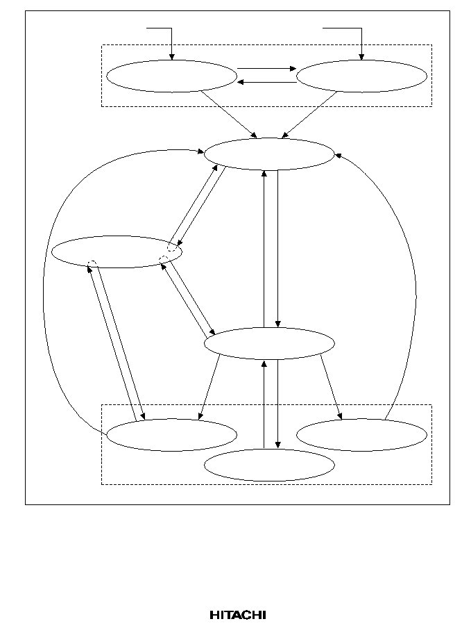
45
RES
= 0, NMI = 1
RES
= 0, NMI = 0
Power-on reset state
Manual reset state
Sleep mode
Standby mode
Program execution state
Module standby
Bus-released state
Exception handling state
RES
= 1,
NMI = 0
RES
= 1,
NMI = 1
Interrupt or DMA
address error
NMI interrupt
Exception
handling
ends
Bus request
generated
Exception
Bus request
cleared
Bus request
generated
Bus request
cleared
SLEEP
instruction with
SBY bit cleared
SLEEP
instruction with
SBY bit set
From any state when
RES
= 0 and NMI = 1
From any state when
RES
= 0 and NMI = 0
Reset state
Power-down state
Bus request
generated
Bus request
cleared
MSTP
bit cleared
MSTP
bit set
Figure 2.6 Transitions between Processing States

46
Reset State: The CPU resets in the reset state. This occurs when the
RES pin level goes low.
When the NMI pin is high, the result is a power-on reset; when it is low, a manual reset will occur.
Exception Handling State: The exception handling state is a transient state that occurs when an
exception handling source such as a reset or interrupt alters the CPU's processing state flow.
For a reset, the initial values of the program counter (PC) (execution start address) and stack
pointer (SP) are fetched from the exception vector table and stored; the CPU then branches to the
execution start address and execution of the program begins.
For an interrupt, the stack pointer (SP) is accessed and the program counter (PC) and status
register (SR) are saved to the stack area. The exception service routine start address is fetched
from the exception processing vector table; the CPU then branches to that address and the program
starts executing, thereby entering the program execution state.
Program Execution State: In the program execution state, the CPU sequentially executes the
program.
Power-Down State: In the power-down state, the CPU operation halts and power consumption
declines. The SLEEP instruction places the CPU in the power-down state. This state has two
modes: sleep mode and standby mode. See section 2.5.2 for more details.
Bus-Released State: In the bus-released state, the CPU releases the bus to the device that has
requested it.
2.5.2
Power-Down State
Besides the ordinary program execution states, the CPU also has a power-down state in which
CPU operation halts, lowering power consumption (table 2.19). There are two power-down state
modes, sleep mode and standby mode, and also a module standby function.
Sleep Mode: When standby bit SBY (in the standby control register SBYCR) is cleared to 0 and a
SLEEP instruction executed, the CPU moves from program execution state to sleep mode. The on-
chip peripheral modules other than the CPU do not halt in the sleep mode. To return from sleep
mode, use a reset, any interrupt, or a DMA address error; the CPU returns to the ordinary program
execution state through the exception handling state.
Software Standby Mode: To enter the standby mode, set the standby bit SBY (in the standby
control register SBYCR) to 1 and execute a SLEEP instruction. In standby mode, all CPU, on-chip
peripheral module, and oscillator functions are halted. When entering the standby mode, confirm
that the DMAC master enable bit is 0. If a multiply instruction is in progress on entry to standby
mode, the MACL and MACH registers will be invalid. CPU internal register contents and on-chip
RAM data are retained. Cache (and on-chip RAM) data is not retained.

47
To return from standby mode, use a reset or an external NMI interrupt. For resets, the CPU returns
to the ordinary program execution state through the exception handling state when placed in a
reset state after the oscillator stabilization time has elapsed. For NMI interrupts, the CPU returns
to the ordinary program execution state through the exception handling state after the oscillator
stabilization time has elapsed. Turn the cache off before entering standby mode. In this mode,
power consumption drops substantially because the oscillator stops.
Module Standby Function: The module standby function is available for the multiplier (MULT),
divider (DIVU), 16-bit free-running timer (FRT), serial communication interface (SCI), and DMA
controller (DMAC) on-chip peripheral modules.
The supply of the clock to these on-chip peripheral modules can be halted by setting the
corresponding bits 40 (MSTP4MSTP0) in the standby control register (SBYCR). By using this
function, the power consumption can be reduced.
The external pins of the on-chip peripheral modules in module standby mode are reset and all
registers except DMAC, MULT, and DIVU are initialized. The module standby function is cleared
by clearing the MSTP4MSTP0 bits to 0.
When MULT has entered the software standby mode, do not execute the DMULS.L, DMULU.L,
MAC.L, MAC.W, MUL.L, MULS, and MULU instructions (all of which are multiply
instructions) or any instructions that access the MACH and MACL registers (CLRMAC, LDS
MACH/MACL, STS MACH/MACL).
When the DMAC module standby function is used, set the DMAC's DMA master enable bit to 0.

48
Table 2.19
Power-Down State
State
Mode
Conditions
Clock
CPU
On-Chip
Peripheral
Modules
CPU
Registers RAM
Canceling
Sleep
Execute
SLEEP
instruction
with SBY bit
cleared to 0
in SBYCR
Active
Halted
Active
Held
Held
1. Interrupt
2. DMA
address
error
3. Power-on
reset
4. Manual
reset
Standby
Execute
SLEEP
instruction
with SBY bit
set to 1 in
SBYCR
Halted
Halted
Halted and
initialized
*1
Held
Undefined 1. NMI
2. Power-on
reset
3. Manual
reset
Module
standby
MSTP4
MSTP0 bits
of SBYCR
set to 1
Active
Active
(MULT
is
halted.)
Supply of clock
to affected
module is halted
and module
initialized.
*2
Held
Held
Clear bits
MSTP 40 of
SBYCR to 0
Notes: 1. Depends on peripheral module and pin.
2. The DMAC, MULT, and DIV registers and the specified interrupt vectors retain their
settings.
49
Section 3 Oscillator Circuits and Operating Modes
3.1
Overview
Operation of the on-chip clock pulse generator, CS0 area bus width specification, and switching
between master and slave modes are controlled by the operating mode pins. A crystal resonator or
external clock can be selected as the clock source.
3.2
On-Chip Clock Pulse Generator and Operating Modes
3.2.1
Clock Pulse Generator
A block diagram of the on-chip clock pulse generator circuit is shown in figure 3.1.
CAP1
CKIO
EXTAL
XTAL
CKPREQ
/
CKM
CKPACK
*
MD2
Clock mode pins
MD1
MD0
Standby
control signal
Clock
PLL circuit 1
Clock mode
control circuit
CAP2
PLL circuit 2
Oscillator
Note: See section 14.4.4, Clock Pause Function
Figure 3.1 Block Diagram of Clock Pulse Generator Circuit

50
Pin Configuration: Table 3.1 lists the functions relating to the pins relating to the oscillator
circuit.
Table 3.1
Pin Functions
Pin Name
I/O
Function
CKIO
I/O
External clock input pin or internal clock output pin
XTAL
O
Connects to the crystal resonator.
EXTAL
I
Connects to the crystal resonator or to the external clock input when
using PLL circuit 2.
CAP1
I
Connects to capacitance for operating PLL circuit 1.
CAP2
I
Connects to capacitance for operating PLL circuit 2.
MD0
I
The level applied to these pins specifies the clock mode.
MD1
I
MD2
I
CKPREQ
/CKM
I
Used as the clock pause request pin, or specifies operation of the crystal
oscillator.
PLL Circuit 1: PLL circuit 1 eliminates phase differences between external clocks and clocks
supplied internally within the chip. In high-speed operation, the phase difference between the
reference clocks and operating clocks in the chip directly affects the interface margin with
peripheral devices
.
On-chip PLL circuit 1 is provided to eliminate this effect.
PLL circuit 1 can also make the phase difference between the clocks 90 degrees, enabling high-
speed interface with synchronous DRAM.
PLL Circuit 2: PLL circuit 2 either leaves unchanged, doubles, or quadruples the frequency of
clocks provided from the crystal resonator or the EXTAL pin external clock input for the chip
operating frequency
.
The frequency modification register sets the clock frequency multiplication
factor.

51
3.2.2
Clock Operating Mode Settings
Table 3.2 lists the functions and operation of clock modes 0 to 6.
Note that TBP-176 package products can only be used in clock modes 4 to 6.
Table 3.2
Operating Modes
Clock Mode
Function/Operation
Clock Source
0
PLL circuits 1 and 2 operate. A clock with the same phase as
the internal chip clock is output from the CKIO pin.
Crystal resonator/
External clock input
1
PLL circuits 1 and 2 operate. A clock shifted 90
°
from the
CKIO pin output is supplied to the internal chip clock.
Crystal resonator/
External clock input
2
Only PLL circuit 2 operates. The clock from PLL circuit 2 is
output from the CKIO pin. Phases are not matched in this
mode.
Crystal resonator/
External clock input
3
Only PLL circuit 2 operates. The CKIO pin is high impedance.
Phases are not matched in this mode.
Crystal resonator/
External clock input
4
Set this mode when the CKIO pin inputs a clock having a
frequency equivalent to the object operating frequency and
PLL circuit 1 synchronizes the phases of the input clock and
the internal clock.
External clock input
5
Set this mode when the CKIO pin inputs a clock having a
frequency equivalent to the object operating frequency and
PLL circuit 1 shifts the phases of the input clock and internal
clock by 90 degrees.
External clock input
6
Set this mode when a clock having a frequency equivalent to
that of clocks input from the CKIO pin are used
.
PLL circuits 1
and 2 do not operate.
External clock input
When clock modes 0 to 3 are selected, the input frequency or its double or quadruple (produced by
PLL circuit 2) is used as the internal clock. When clock modes 4 to 6 are selected, the clock pause
function can modify the frequency of clocks input from the CKIO pin or can stop the sending of
clock signals (see section 14.4, Standby Mode). When clock modes 4 to 6 are set, PLL circuit 2
stops.
Table 3.3 lists the relationship between pins MD2 to MD0 and the clock operating mode. Do not
switch the MD2MD0 pins while they are operating. Switching will cause operating errors.

52
Table 3.3
Clock Mode Pin Settings and States
Pin*
1
Clock
Mode
MD2
MD1
MD0
CKPREQ
/
CKM
EXTAL
XTAL
CKIO
Internal Clock
0
0
0
0
0
1
Clock
input
Crystal
oscillation
Open
Crystal
oscillation
Output
Synchronized to a
phase difference of
0° from CKIO by PLL
circuit 1
1
0
0
1
0
1
Clock
input
Crystal
oscillation
Open
Crystal
oscillation
Output
Synchronized to a
phase difference of
90° from CKIO by
PLL circuit 1
2
0
1
0
0
1
Clock
input
Crystal
oscillation
Open
Crystal
oscillation
Output
CKIO
3
0
1
1
0
1
Clock
input
Crystal
oscillation
Open
Crystal
oscillation
High
impe-
dance
PLL circuit 2 output
4
1
0
0
*
2
Open
Open
Clock
input
Synchronized to a
phase difference of
0° from CKIO by PLL
circuit 1
5
1
0
1
Open
Open
Clock
input
Synchronized to a
phase difference of
90° from CKIO by
PLL circuit 1
6
1
1
0
Open
Open
Clock
input
CKIO
Notes: 1. Do not use in combinations other than those listed.
2. In clock modes 4, 5, and 6,
CKPREQ
/CKM functions as the clock pause request pin.
3. For TBP-176 package products, only clock mode 4, 5, or 6 can be selected.
3.2.3
Connecting a Crystal Resonator
Connecting a Crystal Resonator: Figure 3.2 shows how to connect a crystal resonator. Use the
value shown in table 3.4 for the damping resistance Rd. The crystal resonator should be an AT-cut
parallel-resonance type. Be sure to connect load capacitors (CL1, CL2) as shown in the figure.
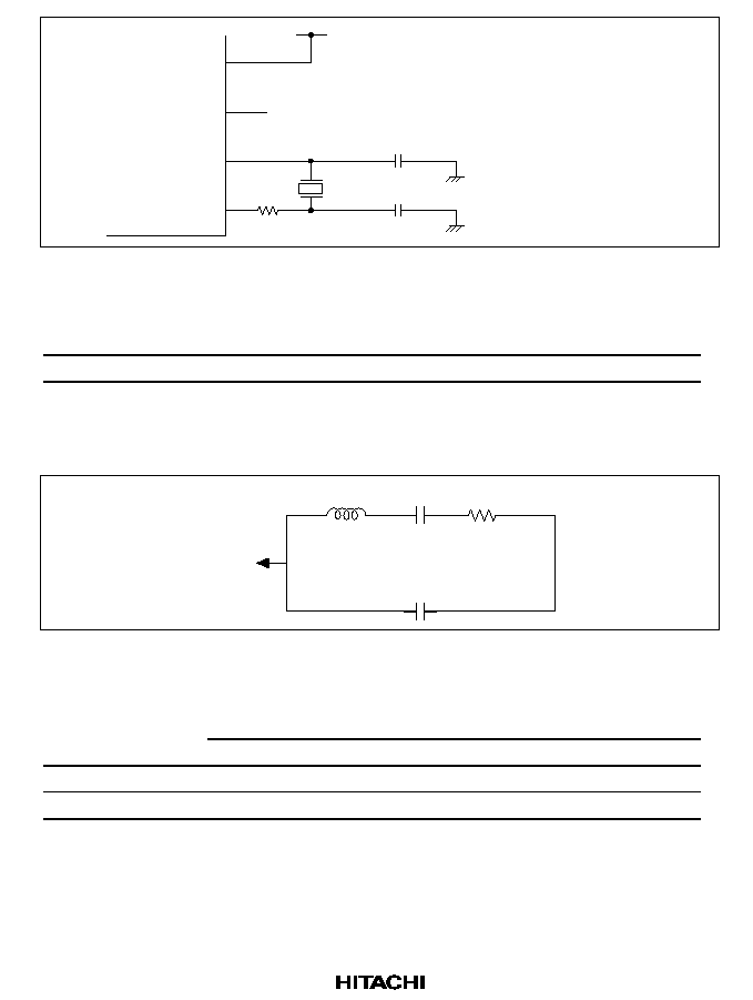
53
High level
The CKIO pin is an output in clock
modes 0,1, and 2. In mode 3,
it is high impedance.
CL1
Rd
CKPREQ
/CKM
CKIO
EXTAL
XTAL
CL1 = CL2 = 18 pF22 pF
Output or high
impedance
CL2
Figure 3.2 Example of Crystal Resonator Connection
Table 3.4
Damping Resistance (Reference Values)
Frequency (MHz)
4
6
8
Rd (
)
500
200
0
Crystal Resonator: Figure 3.3 shows a crystal resonator equivalent circuit. Use a crystal
resonator that has the characteristics shown in table 3.5.
Co
EXTAL
CL
Rs
L
Figure 3.3 Crystal Resonator Equivalent Circuit
Table 3.5
Crystal Resonator Characteristics (Reference Values)
Frequency (MHz)
Parameters
4
6
8
Rs max (
)
120
100
80
Co max (pF)
7 pF max
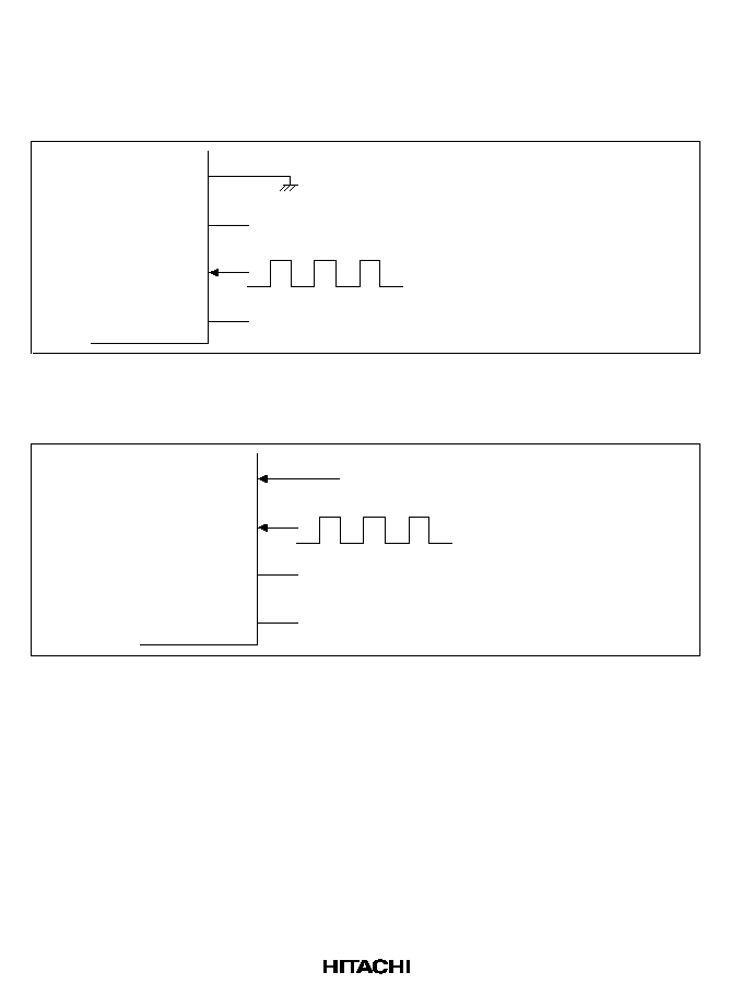
54
3.2.4
Inputting an External Clock
Input the external clock from the EXTAL pin or the CKIO pin, depending on the clock mode.
Clock Input from the EXTAL Pin: This can be used in clock modes 0,1, 2, and 3.
Ground level
The CKIO pin is an output in clock
modes 0,1, and 2. In mode 3,
it is high impedance.
CKPREQ
/CKM
CKIO
EXTAL
XTAL
Output or high
impedance
Open
External clock input
Figure 3.4 Inputting External Clock
Clock Input from the CKIO Pin: This can be used in clock modes 4, 5, and 6.
CKPREQ
/CKM becomes the input
pin for clock pause requests
CKPREQ
/CKM
CKIO
EXTAL
XTAL
Open
Open
External clock input
Figure 3.5 Inputting External Clock
3.2.5
Selecting Operating Frequency with a Register
PLL circuit 2 and the frequency modification register can double or quadruple the operating
frequency in clock modes 0 to 3
.
Figure 3.6 shows a block diagram of PLL circuit 2 and the
frequency modification register.
55
Oscillator
PLL circuit 2
f
×
4
f
×
2
f
×
1
PLL
f
Frequency selection circuit
Frequency
modification register
Data bus
Frequency
divider
Frequency
divider
CAP2
XTAL
EXTAL
Figure 3.6 Relationship between PLL Circuit 2 and the Frequency Modification Register
PLL circuit 2 includes the PLL circuit (which quadruples frequency f of clocks generated by the
oscillator) and frequency dividers, which divide the output of the PLL circuit by 2 or 4. The clocks
(f
×
1, f
×
2, and f
×
4) are input to the frequency selection circuit, where one is selected according
to the value set in the frequency modification register, and is then output from PLL circuit 2.
Frequency Modification Register: This register is only initialized by a power-on reset. It holds
its values in a manual reset and in standby mode. Table 3.6 shows the register configuration, and
the following figure shows the bit combinations and functions.
Table 3.6
Frequency Modification Register
Register
Abbrev.
R/W
Initial Value
Address
Access Size
Frequency modification register
FMR
R/W
H'00
H'FFFFFE90
8
Bit:
7
6
5
4
3
2
1
0
Bit name:
--
--
--
--
--
--
FR1
FR0
Initial value:
0
0
0
0
0
0
0
0
R/W:
R
R
R
R
R
R
R/W
R/W
Bit 1: FR1
Bit 0: FR0
Description
0
0
No multiplication
(Initial value)
1
×
2 multiplication
1
0
×
4 multiplication
1
Setting prohibited
56
Bits 27 are reserved. They always read 0, and the write value should always be 0.
Modifying Frequencies: In the following modifications, the device is running in clock modes 0 to
3, and the operating frequency is left unchanged, doubled, or quadrupled using PLL circuit 2.
·
Set the TME bit to 0 in or above the oscillation settling time that specifies the on-chip WDT's
overflow time.
·
Set the frequency modification register to the target value. (The chip will go internally to
standby mode temporarily.)
·
All circuits involved in oscillation operate and the clock is supplied to the WDT. The WDT
overflows with this clock.
·
When the WDT overflows, a clock at the frequency set within the chip begins to be supplied
and the chip returns from standby mode.
Frequency Modification Guidelines:
·
Only write to the frequency modification register while the cache is disabled.
·
The frequency modification program is always in cache memory and so should be executed
utilizing the forced access space of the data array. Figure 3.7 shows how the frequency
modification register is set.
·
When the frequency modification program is executed, execute an associative or forced purge
of the entries in the data array used.
·
Place at least eight consecutive NOP instructions after an instruction that writes to the
frequency modification register.
Disable cache
Transfer the frequency
modification program
to the data array
Execute the frequency
modification program in
data array forced space
Cache purge
Next program
Figure 3.7 Frequency Modification Flowchart

57
Frequency Modification Register Setting Program (Sample)
; DEFINE CONSTANTS
CLR .EQU H'00000000
WAIT_TIME .EQU H'00080000
PURGE .EQU H'40000000
;
MAP_ROM .EQU H'00000000
MAP-IO .EQU H'FFFFF000
;
DIRECT_RW .EQU H'C0000000
MDC_FLCR .EQU H'FFFFFE90
MDC_CCR .EQU H'FFFFFE92
WTCSR .EQU H'FFFFFE80
;
; Program initialization
MOV.L #CLOCK2_START,R0
MOV.L #DIRECT_RW,R1
MOV.L #CLOCK2_END,R11
; Cache_CCR save, disable, and forced purge
MOV.L #MDC_CCR,R2
MOV.B @R2,R6
MOV #H'00,R3 ;Disable setting
MOV.B R3,@R2
MOV.B @R2,R3 ;Dummy read
MOV #H'10,R3 ;Forced purge setting
MOV.B R3,@R2
;
; Transfer frequency modification program to the data array
;
PRG_TRNS
; Read from the main memory
MOV.L @R0,R2
MOV.L @(4,R0),R3
*1
MOV.L @(8,R0),R4
*1
MOV.L @(12,R0),R5
*1
; Write to the data array
MOV.L R2,@R1

58
MOV.L R3,@(4,R1)
*1
MOV.L R4,@(8,R1)
*1
MOV.L R5,@(12,R1)
*1
; Increment pointer
ADD #H'10,R0
ADD #H'10,R1
; Loop
CMP/GT R11,R0
BF PRG_TRNS
; Branch to the data array forced access space
MOV.L #DIRECT_RW,R0
JMP @R0
NOP
.CONST
*2
;
CLOCK2_START
MOV.L #NEXT_PROG,R3 ;Branch destination address
for the next program
MOV.L #WTCSR,R0 ;WDT setting
MOV.L #H'0000A507,R1 ;Set enough time for PLL to be
stabilized
MOV.W R1,@R0
MOV.L #MDC_FLCR,R2 ;Frequency modification
register setting
MOV #H'01,R1 ;Double the internal frequency
MOV.B R1,@R2
; Wait during frequency modification
NOP
NOP
NOP
NOP
NOP
NOP
NOP
NOP

59
NOP
NOP
NOP
NOP
NOP
NOP
NOP
; Branch to the next program
JMP @R3
NOP
.CONST
*2
CLOCK2_END
;
; Next program
NEXT_PROG
; Cache_CCR load
MOV.L #MDC_CCR,R2
MOV.B R6,@R2
.
.
.
Notes: *1 This example shows Hitachi cross-assembler coding. With the Hitachi cross-assembler,
the values to which scaling (
×
1,
×
2,
×
4) is applied are written. For coding in other cross-
assemblers, see the notation rules.
*2 This is a literal pool output control statement. Code according to the notation rule for the
assembler used. The Hitachi cross-assembler is not required.
*3 When the WTCSR set value is read, H'0000A51F' is returned.

60
3.2.6
Operating Modes and Frequency Ranges
Table 3.7 shows the operating modes and the associated frequency ranges for input clocks.
Table 3.7
Operating Modes and Frequency Ranges
PLL Circuit
Clock Input
Internal
Clock
CKIO
Output
Mode PLL1 PLL2
Pin
Input Frequency
Range (MHz)
Frequency
(MHz)
Frequency
(MHz)
Comments
0
Active Active
EXTAL
48*
1
4 max*
2
7max*
2
Multiplication
1
(including
ratio settable
2
Halted
when resonator
4 max*
2
(
×
1,
×
2,
×
4)
3
is used)
4
Active Halted CKIO
7max*
2
7max*
3
Multiplication
5
not settable
6
Halted
4max*
2
4max*
2
(
×
1 only)
Notes: 1. Make the setting so that the clock frequency output from the CKIO pin does not exceed
the maximum operating frequency. For example, if 8 MHz is input, set the multiplication
ratio of the frequency to
×
1 or
×
2. (If
×
4 is used, a 32-MHz clock is output from the CKIO
pin, which is outside the range for the PLL circuit 1 input frequency.)
2. "max" represents the maximum operating frequency of 28.7 MHz at 5 V operation and
20.0 MHz at 3.3 V operation.
3. If CKIO output below 7 MHz is used during PLL circuit 1 operation, AC characteristics
using the CKIO output are not guaranteed.
3.2.7
Notes on Board Design
When Using a Crystal Resonator: Place the crystal resonator and capacitors as close to the
EXTAL and XTAL pins as possible. Do not let the pins' signal lines cross other signal lines. If
they do, induction may prevent proper oscillation.
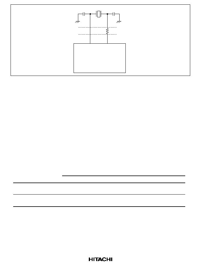
61
EXTAL
XTAL
SH7604
CL1
CL2
CL1 = CL2 = 18 pF22 pF
No crossing of signal lines
Figure 3.8 Design Considerations when Using a Crystal Resonator
When Using PLL Oscillation Circuits: Place oscillation settling capacitors C1 and C2 and
resistors R1 and R2 near the CAP1 and CAP2 pins, and keep the wiring from the CAP pins as
short as possible. As the CAP pin circuits are susceptible to influence by other signals, avoid
crossing signal lines both on the board surface and in internal layers. PLL-V
CC
and PLL-V
SS
should be isolated from other V
CC
and V
SS
lines away from the board's power supply sources, and
bypass capacitors CPB and CB must be inserted near the pins.
In the clock circuits in this product, clock stability may be affected by reflected noise generated by
the CKIO pin. This influence is especially great in clock modes 0 and 1, in which the PLL1 and
PLL2 circuits are used simultaneously, so the board design should ensure that reflected noise does
not occur in CKIO. In clock mode 6, in which no PLLs are used, connect PLL-V
CC
to V
CC
and
PLL-V
SS
to V
SS
.
Table 3.8
Connected Resistance and Capacitance Reference Values
Mode Setting
Resistance/Capacitance
0
1
2
3
4
5
6
R1 = 3 k
C1 = 470 pF
Needed
Needed
Not
needed
Not
needed
Needed
Needed
Not
needed
R2 = 3 k
C2 = 470 pF
Needed
Needed
Needed
Needed
Not
needed
Not
needed
Not
needed
When the PLL circuits are off, CAP1 and CAP2 should be left open or used as shown in the
recommended example.
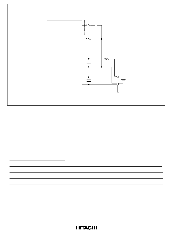
62
No crossing of signal lines
(do not cross signal lines in
adjacent layers on the board)
CAP1
SH7604
CAP2
PLLV
CC
PLLV
SS
V
CC
V
SS
CPB
Rp
R2 C2
R2 C2
CB
Note:
CPB/CB: 0.1
µ
F (laminated ceramic)
Rp: 300
resistance (recommended value)
Figure 3.9 Design Considerations when Using PLL Oscillation Circuits
3.3
Bus Width of the CS0 Area
Pins MD3 and MD4 are used to specify the bus width of the CS0 area (boot ROM area)
.
The pin
combination and functions are listed in table 3.9. Do not switch the MD4 and MD3 pins while
they are operating. Switching them will cause operating errors.
Table 3.9
Bus Width of the CS0 Area
Pin
MD4
MD3
Function
0
0
8-bit bus width selected
0
1
16-bit bus width selected
1
0
32-bit bus width selected
1
1
Setting prohibited

63
3.4
Switching between Master Mode and Slave Mode
The SH7604 has two master modes and a slave mode for bus rights that can be selected with the
MD5 pin. The master modes consist of a total master mode and a partial-share master mode,
which are specified using the MD5 pin and the partial-share space specification bit (PSHR) in bus
control register 1 (BCR1). When the slave mode is selected with the MD5 pin, the device enters
total slave mode. When master mode is selected with the MD5 pin and partial-space share is
specified with the PSHR bit, the device enters partial-share master mode. When partial-space
share is not specified with the PSHR bit, the device enters total master mode.
Total master mode has rights to bus use. External devices can be accessed freely. The bus can be
allocated to another CPU upon request.
Total slave mode does not have any rights to bus use. When an external device is accessed, bus
rights have to be requested from the master CPU, and permission to use the bus gained, before the
external device can be accessed.
Partial-share master mode lacks bus rights only for the CS2 space. To access the CS2 space, bus
rights must first be requested from the master CPU, and permission granted. This mode has bus
rights for all other spaces and does not require a request for the bus when accessing them (table
3.10). Do not change MD5 while external device accesses are in progress.
Table 3.10
Master Modes and Slave Mode
Mode
MD5
Total Slave Mode
Specification Pin
PSHR
Partial-Share
Bit
Function
Total slave
mode
1
(Not used)
Has no bus rights. To use the bus, it must
request the bus and receive permission from
the master CPU.
Partial-share
master mode
0
1
Has bus rights to CS0, CS1, and CS3 spaces,
but not normally to CS2. To access CS2, it
must first request and be granted bus rights.
Total master
mode
0
0
Always has bus rights. Grants bus rights to
slave CPUs.

64

65
Section 4 Exception Handling
4.1
Overview
4.1.1
Types of Exception Handling and Priority Order
Exception handling is initiated by four sources: resets, address errors, interrupts, and instructions
(table 4.1). When several exception handling sources occur at once, they are processed according
to priority.
Table 4.1
Types of Exception Handling and Priority Order
Exception
Source
Priority
Reset
Power-on reset
High
Manual reset
Address
CPU address error
error
DMA address error
Interrupt
NMI
User break
IRL (IRL1IRL15 (set with
IRL3
,
IRL2
,
IRL1
,
IRL0
pins))
On-chip peripheral modules
Division unit (DIVU)
Direct memory access controller (DMAC)
Watchdog timer (WDT)
Compare match interrupt (part of the bus
state controller)
Serial communication interface (SCI)
16-bit free-running timer (FRT)
Instructions Trap instruction (TRAPA)
General illegal instructions (undefined code)
Illegal slot instructions (undefined code placed directly following a delayed
branch instruction
*1
or instructions that rewrite the PC
*2
)
Low
Notes: 1. Delayed branch instructions: JMP, JSR, BRA, BSR, RTS, RTE, BF/S, BT/S, BSRF,
BRAF
2. Instructions that rewrite the PC: JMP, JSR, BRA, BSR, RTS, RTE, BT, BF, TRAPA,
BF/S, BT/S, BSRF, BRAF

66
4.1.2
Exception Handling Operations
Exception handling sources are detected, and exception handling started, according to the timing
shown in table 4.2.
Table 4.2
Timing of Exception Source Detection and Start of Exception Handling
Exception Source
Timing of Source Detection and Start of Handling
Reset
Power-on reset
Starts when the NMI pin is high and the
RES
pin changes from
low to high.
Manual reset
Starts when the NMI pin is low and the
RES
pin changes from
low to high.
Address error
Detected when instruction is decoded and starts when the
previous executing instruction finishes executing.
Interrupts
Detected when instruction is decoded and starts when the
previous executing instruction finishes executing.
Instructions
Trap instruction
Starts from the execution of a TRAPA instruction.
General illegal
instructions
Starts from the decoding of undefined code anytime except after
a delayed branch instruction (delay slot).
Illegal slot
instructions
Starts from the decoding of undefined code placed directly
following a delayed branch instruction (delay slot) or of an
instruction that rewrites the PC.
When exception handling starts, the CPU operates as follows:
1. Exception handling triggered by reset
The initial values of the program counter (PC) and stack pointer (SP) are fetched from the
exception vector table (PC and SP are respectively addresses H'00000000 and H'00000004 for
a power-on reset and addresses H'00000008 and H'0000000C addresses for a manual reset).
See section 4.1.3, Exception Vector Table, for more information. 0 is then written to the vector
base register (VBR) and 1111 is written to the interrupt mask bits (I3I0) of the status register.
The program begins running from the PC address fetched from the exception vector table.
2. Exception handling triggered by address errors, interrupts, and instructions
SR and PC are saved to the stack address indicated by R15. For interrupt exception handling,
the interrupt priority level is written to the SR's interrupt mask bits (I3I0). For address error
and instruction exception handling, the I3I0 bits are not affected. The start address is then
fetched from the exception vector table and the program begins running from that address.

67
4.1.3
Exception Vector Table
Before exception handling begins, the exception vector table must be written in memory. The
exception vector table stores the start addresses of exception service routines. (The reset exception
table holds the initial values of PC and SP.)
All exception sources are given different vector numbers and vector table address offsets, from
which the vector table addresses are calculated. During exception handling, the start addresses of
the exception service routines are fetched from the exception vector table.
Table 4.3 lists the vector numbers and vector table address offsets. Table 4.4 shows vector table
address calculations.
Table 4.3
Exception Vector Table
Exception Source
Vector
Number
Vector Table Address
Offset
Vector Address
Power-on reset
PC
0
H'00000000H'00000003
Vector number
×
4
SP
1
H'00000004H'00000007
Manual reset
PC
2
H'00000008H'0000000B
SP
3
H'0000000CH'0000000F
General illegal instruction
4
H'00000010H'00000013
VBR + (vector
(Reserved by system)
5
H'00000014H'00000017
number
×
4)
Slot illegal instruction
6
H'00000018H'0000001B
(Reserved by system)
7
H'0000001CH'0000001F
8
H'00000020H'00000023
CPU address error
9
H'00000024H'00000027
DMA address error
10
H'00000028H'0000002B
Interrupt
NMI
11
H'0000002CH'0000002F
User break
12
H'00000030H'00000033
(Reserved by system)
13
:
31
H'00000034H'00000037
:
H'0000007CH'0000007F
Trap instruction (user vector)
32
:
63
H'00000080H'00000083
:
H'000000FCH'000000FF

68
Table 4.3
Exception Processing Vector Table (cont)
Exception Source
Vector
Number
Vector Table Address
Offset
Vector Addresses
Interrupt
IRL1
*1
64
*2
H'00000100H'00000103
VBR + (vector
IRL2
*1
65
*2
H'00000104H'00000107
number
×
4)
IRL3
*1
IRL4
*1
66
*2
H'00000108H'0000010B
IRL5
*1
IRL6
*1
67
*2
H'0000010CH'0000010F
IRL7
*1
IRL8
*1
68
*2
H'00000110H'00000113
IRL9
*1
IRL10
*1
69
*2
H'00000114H'00000117
IRL11
*1
IRL12
*1
70
*2
H'00000118H'0000011B
IRL13
*1
IRL14
*1
71
*2
H'0000011CH'0000011F
IRL15
*1
On-chip
peripheral
module*
3
0
*4
:
255
*4
H'00000000H'00000003
:
H'000003FCH'000003FF
Notes: 1. When 1110 is input to the
IRL3
,
IRL2
,
IRL1
, and
IRL0
pins, an IRL1 interrupt results.
When 0000 is input, an IRL15 interrupt results.
2. External vector number fetches can be performed without using the auto-vector
numbers in this table.
3. The vector numbers and vector table address offsets for each on-chip peripheral
module interrupt are given in section 5, Interrupt Controller, and table 5.4, Interrupt
Exception Vectors and Priorities.
4. Vector numbers are set in the on-chip vector number register. See section 5.3,
Description of Registers, section 9, Direct Memory Access Controller, and section 10,
Division Unit, for more information.

69
Table 4.4
Calculating Exception Vector Table Addresses
Exception Source
Vector Table Address Calculation
Power-on reset
Manual reset
(Vector table address) = (vector table address offset)
= (vector number)
×
4
Other exception handling
(Vector table address) = VBR + (vector table address offset)
= VBR + (vector number)
×
4
Note:
VBR: Vector base register
Vector table address offset: See table 4.3.
Vector number: See table 4.3.
4.2
Resets
4.2.1
Types of Resets
Resets have the highest priority of any exception source. There are two types of resets: manual
resets and power-on resets. As table 4.5 shows, both types of resets initialize the internal status of
the CPU. In power-on resets, all registers of the on-chip peripheral modules are initialized; in
manual resets, registers of all on-chip peripheral modules except the bus state controller (BSC),
user break controller (UBC) and frequency modification register are initialized. (Use the power-on
reset when turning the power on.)
Table 4.5
Types of Resets
Conditions for
Transition to Reset Status
Internal Status
Type
NMI Pin
RES
Pin
CPU
On-Chip Peripheral Modules
Power-on reset
High
Low
Initialized
Initialized
Manual reset
Low
Low
Initialized
Initialized except for BSC, UBC,
and FMR register

70
4.2.2
Power-On Reset
When the NMI pin is high and the
RES pin is driven low, the device performs a power-on reset.
For a reliable reset, the
RES pin should be kept low for at least the duration of the oscillation
settling time (when the PLL circuit is halted) or for 20 clock cycles (when the PLL circuit is
running). During a power-on reset, the CPU's internal state and all on-chip peripheral module
registers are initialized. See appendix A, Pin States, for the state of individual pins in the power-on
reset state.
In a power-on reset, power-on reset exception handling starts when the NMI pin is kept high and
the
RES pin is first driven low for a set period of time and then returned to high. The CPU will
then operate as follows:
1. The initial value (execution start address) of the program counter (PC) is fetched from the
exception vector table.
2. The initial value of the stack pointer (SP) is fetched from the exception vector table.
3. The vector base register (VBR) is cleared to H'00000000 and the interrupt mask bits (I3I0) of
the status register (SR) are set to H'F (1111).
4. The values fetched from the exception vector table are set in the PC and SP, and the program
begins executing.
4.2.3
Manual Reset
When the NMI pin is low and the
RES pin is driven low, the device executes a manual reset. For a
reliable reset, the
RES pin should be kept low for at least 20 clock cycles. During a manual reset,
the CPU's internal state is initialized. Registers of all on-chip peripheral modules except the bus
state controller (BSC), user break controller (UBC) and the frequency modification register are
initialized. Since the BSC is not affected, the DRAM and synchronous DRAM refresh control
functions remain operational even if the manual reset state continues for a long period of time.
When the chip enters the manual reset state in the middle of a bus cycle, manual reset exception
handling does not start until the bus cycle has ended. Thus, manual resets do not abort bus cycles.
See appendix A, Pin States, for the state of individual pins in the manual reset state.
In a manual reset, manual reset exception handling starts when the NMI pin is kept low and the
RES pin is first kept low for a set period of time and then returned to high. The CPU will then
operate in the same way as for a power-on reset.

71
4.3
Address Errors
4.3.1
Sources of Address Errors
Address errors occur when instructions are fetched or data read or written, as shown in table 4.6.
Table 4.6
Bus Cycles and Address Errors
Bus Cycle
Type
Bus
Master
Bus Cycle Description
Address Errors
Instruction CPU
Instruction fetched from even address
None (normal)
fetch
Instruction fetched from odd address
Address error occurs
Instruction fetched from other than on-chip peripheral
module space
None (normal)
Instruction fetched from on-chip peripheral module
space
Address error occurs
Data
CPU or
Word data accessed from even address
None (normal)
read/write
DMAC
Word data accessed from odd address
Address error occurs
Longword data accessed from a longword boundary
None (normal)
Longword data accessed from other than a longword
boundary
Address error occurs
Access of cache purge space, address array read/
write space or on-chip I/O space by PC-relative
addressing
Address error occurs
Access of cache purge space, address array read/
write space, data array read/write space or on-chip
I/O space by a TAS.B instruction
Address error occurs
Byte data accessed in on-chip peripheral module
space at addresses H'FFFFFF00 to H'FFFFFFFF
Address error occurs
Word or longword data accessed in on-chip peripheral
module space at addresses H'FFFFFF00 to
H'FFFFFFFF
None (normal)
Longword data accessed in on-chip peripheral module
space at addresses H'FFFFFE00 to H'FFFFFEFF
Address error occurs
Word or byte data accessed in on-chip peripheral
module space at addresses H'FFFFFE00 to
H'FFFFFEFF
None (normal)
Notes: 1. Address errors do not occur during the synchronous DRAM mode register write cycle.
2. 16-byte DMAC transfers use longword accesses.

72
4.3.2
Address Error Exception Handling
When an address error occurs, address error exception handling begins after the end of the bus
cycle in which the error occurred and completion of the executing instruction. The CPU operates
as follows:
1. The status register (SR) is saved to the stack.
2. The program counter (PC) is saved to the stack. The PC value saved is the start address of the
instruction to be executed after the last instruction executed .
3. The exception service routine start address is fetched from the exception vector table entry that
corresponds to the address error that occurred, and the program starts executing from that
address. The jump that occurs is not a delayed branch.
4.4
Interrupts
4.4.1
Interrupt Sources
Table 4.7 shows the sources that initiate interrupt exception handling. These are divided into NMI,
user breaks, IRL, and on-chip peripheral modules. Each interrupt source is allocated a different
vector number and vector table address offset. See table 5.4, Interrupt Exception Vectors and
Priority Order, in section 5, Interrupt Controller, for more information.
Table 4.7
Types of Interrupt Sources
Type
Request Source
Number of Sources
NMI
NMI pin (external input)
1
User break
User break controller
1
IRL
IRL1IRL15 (external input)
15
On-chip peripheral module
Direct memory access controller (DMAC)
2
Division unit (DIVU)
1
Serial communication interface (SCI)
4
Free-running timer (FRT)
3
Watchdog timer (WDT)
1
Bus state controller (BSC)
1

73
4.4.2
Interrupt Priority Levels
The interrupt priority order is predetermined. When multiple interrupts occur simultaneously, the
interrupt controller (INTC) determines their relative priorities and begins exception handling
accordingly.
The priority order of interrupts is expressed as priority levels 016, with priority 0 the lowest and
priority 16 the highest. The NMI interrupt has priority 16 and cannot be masked, so it is always
accepted. The user break interrupt priority level is 15 and IRL interrupts have priorities of 115.
On-chip peripheral module interrupt priority levels can be set freely using the INTC's interrupt
priority level setting registers A and B (IPRA and IPRB) as shown in table 4.8. The priority levels
that can be set are 015. Level 16 cannot be set. For more information on IPRA and IPRB, see
sections 5.3.1 and 5.3.2, Interrupt Priority Level Setting Registers A and B (IPRA and IPRB).
Table 4.8
Interrupt Priority Order
Type
Priority Level Comment
NMI
16
Fixed priority level. Cannot be masked.
User break
15
Fixed priority level.
IRL
115
Set with
IRL3
IRL0
pins.
On-chip peripheral module
015
Set with interrupt priority level setting registers A and
B (IPRA and IPRB).
4.4.3
Interrupt Exception Handling
When an interrupt occurs, its priority level is ascertained by the interrupt controller (INTC). NMI
is always accepted, but other interrupts are only accepted if they have a priority level higher than
the priority level set in the interrupt mask bits (I3I0) of the status register (SR).
When an interrupt is accepted, exception handling begins. In interrupt exception handling, the
CPU saves SR and the program counter (PC) to the stack. The priority level value of the accepted
interrupt is written to SR bits I3I0. For NMI, however, the priority level is 16, but the value set in
I3I0 is H'F (level 15). Next, the start address of the exception service routine is fetched from the
exception vector table for the accepted interrupt, that address is jumped to and execution begins.
For more information about interrupt exception handling, see section 5.4, Interrupt Operation.

74
4.5
Exceptions Triggered by Instructions
4.5.1
Instruction-Triggered Exception Types
Exception handling can be triggered by a trap instruction, general illegal instruction or illegal slot
instruction, as shown in table 4.9.
Table 4.9
Types of Exceptions Triggered by Instructions
Type
Source Instruction
Comment
Trap instruction
TRAPA
--
Illegal slot
instruction
Undefined code placed
immediately after a delayed
branch instruction (delay slot)
and instructions that rewrite the
PC
Delayed branch instructions: JMP, JSR,
BRA, BSR, RTS, RTE, BF/S, BT/S, BSRF,
BRAF
Instructions that rewrite the PC: JMP, JSR,
BRA, BSR, RTS, RTE, BT, BF, TRAPA,
BF/S, BT/S, BSRF, BRAF
General illegal
instruction
Undefined code anywhere
besides in a delay slot
--
4.5.2
Trap Instructions
When a TRAPA instruction is executed, trap instruction exception handling starts. The CPU
operates as follows:
1. The status register (SR) is saved to the stack.
2. The program counter (PC) is saved to the stack. The PC value saved is the start address of the
instruction to be executed after the TRAPA instruction.
3. The exception service routine start address is fetched from the exception vector table entry that
corresponds to the vector number specified by the TRAPA instruction. That address is jumped
to and the program starts executing. The jump that occurs is not a delayed branch.
4.5.3
Illegal Slot Instructions
An instruction placed immediately after a delayed branch instruction is said to be placed in a delay
slot. If the instruction placed in the delay slot is undefined code, illegal slot exception handling
begins when the undefined code is decoded. Illegal slot exception handling also starts up when an
instruction that rewrites the program counter (PC) is placed in a delay slot. The exception handling
starts when the instruction is decoded. The CPU handles an illegal slot instruction as follows:

75
1. The status register (SR) is saved to the stack.
2. The program counter (PC) is saved to the stack. The PC value saved is the jump address of the
delayed branch instruction immediately before the undefined code or the instruction that
rewrites the PC.
3. The exception service routine start address is fetched from the exception vector table entry that
corresponds to the exception that occurred. That address is jumped to and the program starts
executing. The jump that occurs is not a delayed branch.
4.5.4
General Illegal Instructions
When undefined code placed anywhere other than immediately after a delayed branch instruction
(i.e., in a delay slot) is decoded, general illegal instruction exception handling starts. The CPU
handles general illegal instructions in the same way as illegal slot instructions. Unlike processing
of illegal slot instructions, however, the program counter value stored is the start address of the
undefined code.
4.6
When Exception Sources are Not Accepted
When an address error or interrupt is generated after a delayed branch instruction or interrupt-
disabled instruction, it is sometimes not immediately accepted but is stored instead, as described in
table 4.10. When this happens, it will be accepted when an instruction for which exception
acceptance is possible is decoded.
Table 4.10
Exception Source Generation Immediately after a Delayed Branch Instruction
or Interrupt-Disabled Instruction
Exception Source
Point of Occurrence
Address Error
Interrupt
Immediately after a delayed branch instruction
*1
Not accepted
Not accepted
Immediately after an interrupt-disabled instruction
*2
Accepted
Not accepted
Notes: 1. Delayed branch instructions: JMP, JSR, BRA, BSR, RTS, RTE, BF/S, BT/S, BSRF,
BRAF
2. Interrupt-disabled instructions: LDC, LDC.L, STC, STC.L, LDS, LDS.L, STS, STS.L
4.6.1
Immediately after a Delayed Branch Instruction
When an instruction placed immediately after a delayed branch instruction (delay slot) is decoded,
neither address errors nor interrupts are accepted. The delayed branch instruction and the
instruction located immediately after it (delay slot) are always executed consecutively, so no
exception handling occurs between the two.

76
4.6.2
Immediately after an Interrupt-Disabled Instruction
When an instruction immediately following an interrupt-disabled instruction is decoded, interrupts
are not accepted. Address errors are accepted.
4.7
Stack Status after Exception Handling
The status of the stack after exception handling ends is as shown in table 4.11.
Table 4.11
Stack Status after Exception Handling
Type
Stack Status
Address error
SP
Address of instruction after executed instruction
32 bits
SR
32 bits
Trap instruction
SP
Address of instruction after TRAPA instruction
32 bits
SR
32 bits
General illegal instruction SP
Start address of illegal instruction
32 bits
SR
32 bits
Interrupt
SP
Address of instruction after executed instruction
32 bits
SR
32 bits
Illegal slot instruction
SP
Jump destination address of delayed branch instruction 32 bits
SR
32 bits
4.8
Usage Notes
4.8.1
Value of Stack Pointer (SP)
The value of the stack pointer must always be a multiple of four, otherwise an address error will
occur when the stack is accessed during exception handling.
4.8.2
Value of Vector Base Register (VBR)
The value of the vector base register must always be a multiple of four, otherwise an address error
will occur when the vector table is accessed during exception handling.

77
4.8.3
Address Errors Caused by Stacking of Address Error Exception Handling
If the stack pointer value is not a multiple of four, an address error will occur during stacking of
the exception handling (interrupts, etc.). Address error exception handling will begin as soon as
the first exception handling is ended, but address errors will continue to occur. To ensure that
address error exception handling does not go into an endless loop, no address errors are accepted
at that point. This allows program control to be shifted to the address error exception service
routine and enables error handling to be carried out.
When an address error occurs during exception handling stacking, the stacking bus cycle (write) is
executed. In stacking of the status register (SR) and program counter (PC), the SP is decremented
by 4 for both, so the value of SP will not be a multiple of four after the stacking either. The
address value output during stacking is the SP value, so the address where the error occurred is
itself output. This means that the write data stacked will be undefined.
4.8.4
Manual Reset during Register Access
Do not initiate a manual reset during access of a bus state controller (BSC) or user break controller
(UBC) register, otherwise a write error may result.

78

79
Section 5 Interrupt Controller (INTC)
5.1
Overview
The interrupt controller (INTC) ascertains the priority of interrupt sources and controls interrupt
requests to the CPU. The INTC has registers for setting the priority of each interrupt which allow
the user to set the order of priority in which interrupt requests are handled.
5.1.1
Features
The INTC has the following features:
·
16 interrupt priority levels: By setting the two interrupt-priority level registers, the priorities of
on-chip peripheral module interrupts can be set at 16 levels for different request sources.
·
Settable vector numbers for on-chip peripheral module interrupts: two vector number setting
registers enable on-chip peripheral module interrupt vector numbers to be set in the range 0
127 by interrupt source.
·
The IRL interrupt vector number setting method can be selected: Either of two modes can be
selected by a register setting: auto-vector mode in which vector numbers are determined
internally, and external vector mode in which vector numbers are set externally.
5.1.2
Block Diagram
Figure 5.1 shows a block diagram of the INTC.
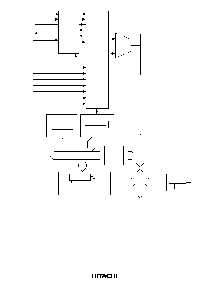
80
CPU
SR
Interrupt request
Com-
parator
Priority
decision
logic
(Interrupt request)
(Interrupt request)
(Interrupt request)
(Interrupt request)
(Interrupt request)
(Interrupt request)
(Interrupt request)
ICR
IPR
IPRA, IPRB
VCRWDT, VCRAVCRD
Module bus
Bus
interface
Internal bus
I3
I2
I1
I0
INTC
NMI
IR3
IR0
A3A0
IVECF
D7D0
UBC
DMAC
DIVU
FRT
SCI
WDT
REF
Input/
output
control
Vector
number
Vector
number
VCRWDT
DIV
DMAC
Peripheral bus
UBC:
User break controller
ICR:
Interrupt control register
DMAC: Direct memory access controller
IPRA/B:
Interrupt priority level setting
DIVU:
Division unit
registers A and B
FRT:
Free-running timer
VCRWDT: Vector number setting register WDT
SCI:
Serial communication interface
VCRAD:
Vector number setting registers AD
WDT:
Watchdog timer
SR:
Status register
REF:
Refresh request within bus state controller
Figure 5.1 INTC Block Diagram

81
5.1.3
Pin Configuration
Table 5.1 shows the INTC pin configuration.
Table 5.1
Pin Configuration
Name
Abbreviation
I/O
Function
Nonmaskable interrupt input pin
NMI
I
Input of nonmaskable interrupt request
signal
Level request interrupt input pins
IRL3
IRL0
I
Input of maskable interrupt request
signals
Interrupt acceptance level output
pins
A3A0
O
In external vector mode, output an
interrupt level signal when an IRL
interrupt is accepted
External vector fetch pin
IVECF
O
Indicates external vector read cycle
External vector number input pins
D7D0
I
Input external vector number
5.1.4
Register Configuration
The INTC has the eight registers shown in table 5.2. These registers perform various INTC
functions including setting interrupt priority, and controlling external interrupt input signal
detection.

82
Table 5.2
Register Configuration
Name
Abbr.
R/W
Initial
Value
Address
Access
Size*
Interrupt priority level setting register A
IPRA
R/W
H'0000
H'FFFFFEE2
8, 16
Interrupt priority level setting register B
IPRB
R/W
H'0000
H'FFFFFE60
8, 16
Vector number setting register A
VCRA
R/W
H'0000
H'FFFFFE62
8, 16
Vector number setting register B
VCRB
R/W
H'0000
H'FFFFFE64
8, 16
Vector number setting register C
VCRC
R/W
H'0000
H'FFFFFE66
8, 16
Vector number setting register D
VCRD
R/W
H'0000
H'FFFFFE68
8, 16
Vector number setting register WDT
VCRWDT
R/W
H'0000
H'FFFFFEE4
8, 16
Vector number setting register DIV
VCRDIV
R/W
--
H'FFFFFF0C
32
Vector number setting register DMAC0
VCRDMA0 R/W
--
H'FFFFFFA0
32
Vector number setting register DMAC1
VCRDMA1 R/W
--
H'FFFFFFA8
32
Interrupt control register
ICR
R/W
H'8000/
H'0000*
H'FFFFFEE0
8, 16
--: Undefined
Note:
The value when the NMI pin is high is H'8000; when the NMI pin is low, it is H'0000.
See the sections 9, Direct Memory Access Controller, and 10, Division Unit, for more
information on VCRDIV, VCRDMA0, and VCRDMA1.
5.2
Interrupt Sources
There are four types of interrupt sources: NMI, user breaks, IRL, and on-chip peripheral modules.
Each interrupt has a priority expressed as a priority level (0 to 16, with 0 the lowest and 16 the
highest). Giving an interrupt a priority level of 0 masks it.
5.2.1
NMI Interrupt
The NMI interrupt has priority 16 and is always accepted. Input at the NMI pin is detected by
edge. Use the NMI edge select bit (NMIE) in the interrupt control register (ICR) to select either
the rising or falling edge. NMI interrupt exception handling sets the interrupt mask level bits (I3
I0) in the status register (SR) to level 15.
5.2.2
User Break Interrupt
A user break interrupt has priority level 15 and occurs when the break condition set in the user
break controller (UBC) is satisfied. User break interrupt exception handling sets the interrupt mask
level bits (I3I0) in the status register (SR) to level 15. For more information about the user break
interrupt, see section 6, User Break Controller.

83
5.2.3
IRL Interrupts
IRL interrupts are requested by input from pins
IRL3IRL0. Fifteen interrupts, IRL15IRL1, can
be input externally via pins
IRL3IRL0. The priority levels of interrupts IRL15IRL0 are 151,
respectively, and their vector numbers are 7164. Set the vector numbers with the IRL interrupt
vector mode select (VECMD) bit of the interrupt control register (ICR) to enable external input.
External input of vector numbers consists of vector numbers 0127 from the external vector input
pins (D7D0). Internal vectors are called auto-vectors and vectors input externally are called
external vectors. Table 5.3 lists IRL priority levels and auto vector numbers.
When an IRL interrupt is accepted in external vector mode, the IRL interrupt level is output from
the interrupt acceptance level output pins (A3A0). The external vector fetch pin (
IVECF) is also
asserted. The external vector number is read from pins D7D0 at this time. Figures 5.2 and 5.3
show interrupt connection examples.
IRL interrupt exception processing sets the interrupt mask level bits (I3 to I0) in the status register
(SR) to the priority level value of the IRL interrupt that was accepted.
Table 5.3
IRL Interrupt Priority Levels and Auto-Vector Numbers
Pin
Priority
Vector
IRL3
IRL2
IRL1
IRL0
Level
Number
0
0
0
0
15
71
0
0
0
1
14
0
0
1
0
13
70
0
0
1
1
12
0
1
0
0
11
69
0
1
0
1
10
0
1
1
0
9
68
0
1
1
1
8
1
0
0
0
7
67
1
0
0
1
6
1
0
1
0
5
66
1
0
1
1
4
1
1
0
0
3
65
1
1
0
1
2
1
1
1
0
1
64
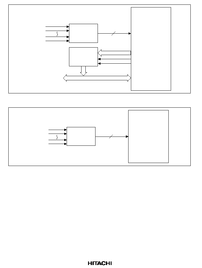
84
SH7604
Priority
encoder
Interrupt
requests
Vector number
generator
circuit
4
IRL0
IRL3
IRL0
IRL3
D0D7
A0A3
IVECF
RD
D0D7
Figure 5.2 Example of Connections for External Vector Mode Interrupts
SH7604
Priority
encoder
Interrupt
requests
4
IRL0
IRL3
IRL0
IRL3
Figure 5.3 Example of Connections for Auto-Vector Mode Interrupts
Figure 5.4 shows the interrupt fetch cycle for the external vector mode. During this cycle,
CS0
CS3 stay high. A26A4 output undefined values. The WAIT pin is sampled, but programmable
waits are not valid.
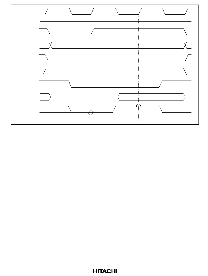
85
CKIO
CS0
CS3
BS
A3A0
Interrupt priority level
IVECF
RD/
WR
RD
D7D0
Vector number input
WAIT
Figure 5.4 External Vector Mode Interrupt Vector Fetch Cycle
5.2.4
On-chip Peripheral Module Interrupts
On-chip peripheral module interrupts are interrupts generated by the following 6 on-chip
peripheral modules:
·
Division unit (DIVU)
·
Direct memory access controller (DMAC)
·
Serial communication interface (SCI)
·
Bus state controller (BSC)
·
Watchdog timer (WDT)
·
Free-running timer (FRT)
A different interrupt vector is assigned to each interrupt source, so the exception service routine
does not have to decide which interrupt has occurred. Priority levels between 0 and 15 can be
assigned to individual on-chip peripheral modules in interrupt priority registers A and B (IPRA
and IPRB). On-chip peripheral module interrupt exception handling sets the interrupt mask level
bits (I3I0) in the status register (SR) to the priority level value of the on-chip peripheral module
interrupt that was accepted.

86
5.2.5
Interrupt Exception Vectors and Priority Order
Table 5.4 lists interrupt sources and their vector numbers, vector table address offsets and interrupt
priorities.
Each interrupt source is allocated a different vector number and vector table address offset. Vector
table addresses are calculated from vector numbers and address offsets. In interrupt exception
handling, the exception service routine start address is fetched from the vector table entry
indicated by the vector table address. See table 4.4, Calculating Exception Vector Table
Addresses, for more information on this calculation.
IRL interrupts IRL15IRL1 have interrupt priority levels of 151, respectively. On-chip peripheral
module interrupt priorities can be set freely between 0 and 15 for each module by setting interrupt
priority registers A and B (IPRA and IPRB). The ranking of interrupt sources for IPRA and IPRB,
however, must be the order listed under Priority Within IPR Setting Unit in table 5.4 and cannot
be changed. A reset assigns priority level 0 to on-chip peripheral module interrupts. If the same
priority level is assigned to two or more interrupt sources and interrupts from those sources occur
simultaneously, their priority order is the default priority order indicated at the right in table 5.4.

87
Table 5.4
Interrupt Exception Vectors and Priority Order
Interrupt
Priority
Order
Priority
within
IPR
Vectors
Interrupt Source
(Initial
Value)
IPR (Bit
Numbers)
Setting
Unit
Vector
No.
Vector Table
Address
Default
Priority
NMI
16
--
--
11
VBR + (vector
High
User break
15
--
--
12
No.
×
4)
IRL15
15
--
--
71
*1
IRL14
14
--
--
IRL13
13
--
--
70
*1
IRL12
12
--
--
IRL11
11
--
--
69
*1
IRL10
10
--
--
IRL9
9
--
--
68
*1
IRL8
8
--
--
IRL7
7
--
--
67
*1
IRL6
6
--
--
IRL5
5
--
--
66
*1
IRL4
4
--
--
IRL3
3
--
--
65
*1
IRL2
2
--
--
IRL1
1
--
--
64
*1
DIVU
OVFI
015 (0)
IPRA (1512)
0127
*2
Low

88
Table 5.4
Interrupt Exception Vectors and Priority Order (cont)
Interrupt
Priority
Order
Priority
within
IPR
Vectors
Interrupt Source
(Initial
Value)
IPR (Bit
Numbers)
Setting
Unit
Vector
No.
Vector Table
Address
Default
Priority
DMAC0
Transfer end
015 (0)
IPRA (118)
1
0127
*2
VBR + (vector
DMAC1
Transfer end
0
0127
*2
No.
×
4)
WDT
ITI
015 (0)
IPRA (74)
1
0127
*2
REF
*3
CMI
0
0127
*2
SCI
ERI
015 (0)
IPRB (1512) 3
0127
*2
RXI
2
0127
*2
TXI
1
0127
*2
TEI
0
0127
*2
FRT
ICI
015 (0)
IPRB (118)
2
0127
*2
OCI
1
0127
*2
OVI
0
0127
*2
Reserved
--
--
--
128255 --
Low
Notes: 1. An external vector number fetch can be performed without using the auto-vector
numbers shown in this table. The external vector numbers are 0127.
2. Vector numbers are set in the on-chip vector number register.
3. REF is the refresh control unit within the bus state controller.
5.3
Description of Registers
5.3.1
Interrupt Priority Level Setting Register A (IPRA)
Interrupt priority level setting register A (IPRA) is a 16-bit read/write register that assigns priority
levels from 0 to 15 to on-chip peripheral module interrupts. IPRA is initialized to H'0000 by a
reset. It is not initialized in standby mode. Unless otherwise specified, `reset' refers to both power-
on and manual resets throughout this manual.

89
Bit:
15
14
13
12
11
10
9
8
Bit name:
DIVU
IP3
DIVU
IP2
DIVU
IP1
DIVU
IP0
DMAC
IP3
DMAC
IP2
DMAC
IP1
DMAC
IP0
Initial value:
0
0
0
0
0
0
0
0
R/W:
R/W
R/W
R/W
R/W
R/W
R/W
R/W
R/W
Bit:
7
6
5
4
3
2
1
0
Bit name:
WDT
IP3
WDT
IP2
WDT
IP1
WDT
IP0
--
--
--
--
Initial value:
0
0
0
0
0
0
0
0
R/W:
R/W
R/W
R/W
R/W
R
R
R
R
·
Bits 15 to 12--Division Unit (DIVU) Interrupt Priority Level (DIVUIP3DIVUIP0): These
bits set the division unit (DIVU) interrupt priority level. There are four bits, so levels 015 can
be set.
·
Bits 11 to 8--DMA Controller Interrupt Priority Level (DMACIP3DMACIP0): These bits set
the DMA controller (DMAC) interrupt priority level. There are four bits, so levels 015 can be
set. The same level is set for both DMAC channels. When interrupts occur simultaneously,
channel 0 has priority.
·
Bits 7 to 4--Watchdog Timer (WDT) Interrupt Priority Level (WDTIP3WDTIP0): These bits
set the watchdog timer (WDT) interrupt priority level and bus state controller (BSC) interrupt
priority level. There are four bits, so levels 015 can be set. When WDT and BSC interrupts
occur simultaneously, the WDT interrupt has priority.
·
Bits 3 to 0--Reserved: These bits always read 0. The write value should always be 0.
5.3.2
Interrupt Priority Level Setting Register B (IPRB)
Interrupt priority level setting register B (IPRB) is a 16-bit read/write register that assigns priority
levels from 0 to 15 to on-chip peripheral module interrupts. IPRB is initialized to H'0000 by a
reset. It is not initialized in standby mode.

90
Bit:
15
14
13
12
11
10
9
8
Bit name:
SCIIP3
SCIIP2
SCIIP1
SCIIP0
FRTIP3
FRTIP2
FRTIP1 FRTIP0
Initial value:
0
0
0
0
0
0
0
0
R/W:
R/W
R/W
R/W
R/W
R/W
R/W
R/W
R/W
Bit:
7
6
5
4
3
2
1
0
Bit name:
--
--
--
--
--
--
--
--
Initial value:
0
0
0
0
0
0
0
0
R/W:
R
R
R
R
R
R
R
R
·
Bits 15 to 12--Serial Communication Interface (SCI) Interrupt Priority Level (SCIIP3
SCIIP0): These bits set the serial communication interface (SCI) interrupt priority level. There
are four bits, so levels 015 can be set.
·
Bits 11 to 8--Free-Running Timer (FRT) Interrupt Priority Level (FRTIP3FRTIP0): These
bits set the free-running timer (FRT) interrupt priority level. There are four bits, so levels 015
can be set.
·
Bits 7 to 0--Reserved: These bits always read 0. The write value should always be 0.
Table 5.5 shows the relationship between on-chip peripheral module interrupts and interrupt
priority level setting registers.
Table 5.5
Interrupt Request Sources and IPRA/IPRB
Register
Bits 15 to 12
Bits 11 to 8
Bits 7 to 4
Bits 3 to 0
IPRA
DIVU
DMAC0, DMAC1
WDT
Reserved
IPRB
SCI
FRT
Reserved
Reserved
As table 5.5 shows, two or three on-chip peripheral modules are assigned to each interrupt priority
register. Set the priority levels by setting the corresponding 4-bit groups (bits 15 to 12, bits 11 to 8,
and bits 7 to 4) with values in the range of H'0 (0000) to H'F (1111). H'0 is interrupt priority level
0 (the lowest); H'F is level 15 (the highest). When two on-chip peripheral modules are assigned to
the same bits (DMAC0 and DMAC1, or WDT and DRAM refresh control unit), those two
modules have the same priority. A reset initializes IPRA and IPRB to H'0000. They are not
initialized in standby mode.

91
5.3.3
Vector Number Setting Register WDT (VCRWDT)
Vector number setting register WDT (VCRWDT) is a 16-bit read/write register that sets the WDT
interval interrupt and BSC compare match interrupt vector numbers (0127). VCRWDT is
initialized to H'0000 by a reset. It is not initialized in standby mode.
Bit:
15
14
13
12
11
10
9
8
Bit name:
--
WITV6
WITV5
WITV4
WITV3
WITV2
WITV1
WITV0
Initial value:
0
0
0
0
0
0
0
0
R/W:
R
R/W
R/W
R/W
R/W
R/W
R/W
R/W
Bit:
7
6
5
4
3
2
1
0
Bit name:
--
BCMV6 BCMV5
BCMV4 BCMV3
BCMV2
BCMV1 BCMV0
Initial value:
0
0
0
0
0
0
0
0
R/W:
R
R/W
R/W
R/W
R/W
R/W
R/W
R/W
·
Bits 15, 7--Reserved: These bits always read 0. The write value should always be 0.
·
Bits 14 to 8--Watchdog Timer (WDT) Interval Interrupt Vector Number (WITV6WITV0):
These bits set the vector number for the interval interrupt (ITI) of the watchdog timer (WDT).
There are seven bits, so the value can be set between 0 and 127.
·
Bits 6 to 0--Bus State Controller (BSC) Compare Match Interrupt Vector Number (BCMV6
BCMV0): These bits set the vector number for the compare match interrupt (CMI) of the bus
state controller (BSC). There are seven bits, so the value can be set between 0 and 127.
5.3.4
Vector Number Setting Register A (VCRA)
Vector number setting register A (VCRA) is a 16-bit read/write register that sets the SCI receive-
error interrupt and receive-data-full interrupt vector numbers (0127). VCRA is initialized to
H'0000 by a reset. It is not initialized in standby mode.

92
Bit:
15
14
13
12
11
10
9
8
Bit name:
--
SERV6
SERV5
SERV4
SERV3
SERV2
SERV1
SERV0
Initial value:
0
0
0
0
0
0
0
0
R/W:
R
R/W
R/W
R/W
R/W
R/W
R/W
R/W
Bit:
7
6
5
4
3
2
1
0
Bit name:
--
SRXV6
SRXV5
SRXV4
SRXV3
SRXV2
SRXV1
SRXV0
Initial value:
0
0
0
0
0
0
0
0
R/W:
R
R/W
R/W
R/W
R/W
R/W
R/W
R/W
·
Bits 15, 7--Reserved: These bits always read 0. The write value should always be 0.
·
Bits 14 to 8--Serial Communication Interface (SCI) Receive-Error Interrupt Vector Number
(SERV6SERV0): These bits set the vector number for the serial communication interface
(SCI) receive-error interrupt (ERI). There are seven bits, so the value can be set between 0 and
127.
·
Bits 6 to 0--Serial Communication Interface (SCI) Receive-Data-Full Interrupt Vector
Number (SRXV6SRXV0): These bits set the vector number for the serial communication
interface (SCI) receive-data-full interrupt (RXI). There are seven bits, so the value can be set
between 0 and 127.
5.3.5
Vector Number Setting Register B (VCRB)
Vector number setting register B (VCRB) is a 16-bit read/write register that sets the SCI transmit-
data-empty interrupt and transmit-end interrupt vector numbers (0127). VCRB is initialized to
H'0000 by a reset. It is not initialized in standby mode.
Bit:
15
14
13
12
11
10
9
8
Bit name:
--
STXV6
STXV5
STXV4
STXV3
STXV2
STXV1
STXV0
Initial value:
0
0
0
0
0
0
0
0
R/W:
R
R/W
R/W
R/W
R/W
R/W
R/W
R/W
Bit:
7
6
5
4
3
2
1
0
Bit name:
--
STEV6
STEV5
STEV4
STEV3
STEV2
STEV1
STEV0
Initial value:
0
0
0
0
0
0
0
0
R/W:
R
R/W
R/W
R/W
R/W
R/W
R/W
R/W

93
·
Bits 15, 7--Reserved: These bits always read 0. The write value should always be 0.
·
Bits 14 to 8--Serial Communication Interface (SCI) Transmit-Data-Empty Interrupt Vector
Number (STXV6STXV0): These bits set the vector number for the serial communication
interface (SCI) transmit-data-empty interrupt (TXI). There are seven bits, so the value can be
set between 0 and 127.
·
Bits 6 to 0--Serial Communication Interface (SCI) Transmit-End Interrupt Vector Number
(STEV6STEV0): These bits set the vector number for the serial communication interface
(SCI) transmit-end interrupt (TEI). There are seven bits, so the value can be set between 0 and
127.
5.3.6
Vector Number Setting Register C (VCRC)
Vector number setting register C (VCRC) is a 16-bit read/write register that sets the FRT input-
capture interrupt and output-compare interrupt vector numbers (0127). VCRC is initialized to
H'0000 by a reset. It is not initialized in standby mode.
Bit:
15
14
13
12
11
10
9
8
Bit name:
--
FICV6
FICV5
FICV4
FICV3
FICV2
FICV1
FICV0
Initial value:
0
0
0
0
0
0
0
0
R/W:
R
R/W
R/W
R/W
R/W
R/W
R/W
R/W
Bit:
7
6
5
4
3
2
1
0
Bit name:
--
FOCV6
FOCV5
FOCV4
FOCV3
FOCV2
FOCV1
FOCV0
Initial value:
0
0
0
0
0
0
0
0
R/W:
R
R/W
R/W
R/W
R/W
R/W
R/W
R/W
·
Bits 15, 7--Reserved: These bits always read 0. The write value should always be 0.
·
Bits 14 to 8--Free-Running Timer (FRT) Input-Capture Interrupt Vector Number (FICV6
FICV0): These bits set the vector number for the free-running timer (FRT) input-capture
interrupt (ICI). There are seven bits, so the value can be set between 0 and 127.
·
Bits 6 to 0--Free-Running Timer (FRT) Output-Compare Interrupt Vector Number (FOCV6
FOCV0): These bits set the vector number for the free-running timer (FRT) output-compare
interrupt (OCI). There are seven bits, so the value can be set between 0 and 127.

94
5.3.7
Vector Number Setting Register D (VCRD)
Vector number setting register D (VCRD) is a 16-bit read/write register that sets the FRT overflow
interrupt vector number (0127). VCRD is initialized to H'0000 by a reset. It is not initialized in
standby mode.
Bit:
15
14
13
12
11
10
9
8
Bit name:
--
FOVV6
FOVV5
FOVV4
FOVV3
FOVV2
FOVV1
FOVV0
Initial value:
0
0
0
0
0
0
0
0
R/W:
R
R/W
R/W
R/W
R/W
R/W
R/W
R/W
Bit:
7
6
5
4
3
2
1
0
Bit name:
--
--
--
--
--
--
--
--
Initial value:
0
0
0
0
0
0
0
0
R/W:
R
R
R
R
R
R
R
R
·
Bits 15, 70--Reserved: These bits always read 0. The write value should always be 0.
·
Bits 14 to 8--Free-Running Timer (FRT) Overflow Interrupt Vector Number (FOVV6
FOVV0): These bits set the vector number for the free-running timer (FRT) overflow interrupt
(OVI). There are seven bits, so the value can be set between 0 and 127.
Tables 5.6 and 5.7 show the relationship between on-chip peripheral module interrupts and
interrupt vector number setting registers.
Table 5.6
Interrupt Request Sources and Vector Number Setting Registers (1)
Bits
Register
148
60
Vector number setting register
WDT
Interval interrupt (WDT)
Compare-match interrupt (BSC)
Vector number setting register A
Receive-error interrupt (SCI) Receive-data-full interrupt (SCI)
Vector number setting register B
Transmit-data-empty interrupt
(SCI)
Transmit-end interrupt (SCI)
Vector number setting register C
Input-capture interrupt (FRT) Output-compare interrupt (FRT)
Vector number setting register D
Overflow interrupt (FRT)
Reserved

95
As table 5.6 shows, two on-chip peripheral module interrupts are assigned to each register. Set the
vector numbers by setting the corresponding 7-bit groups (bits 14 to 8 and bits 6 to 0) with values
in the range of H'00 (0000000) to H'7F (1111111). H'00 is vector number 0 (the lowest); H'7F is
vector number 127 (the highest). The vector table address is calculated by the following equation.
Vector table address = VBR + (vector number
×
4)
A reset initializes a vector number setting register to H'0000. They are not initialized in standby
mode.
Table 5.7 lists functions for vector number setting registers DIV, DMAC0, and DMAC1. The
vector number for DIV overflow interrupts is set in VCRDIV and the vector numbers for DMAC
transfer-end interrupts are set in VCRDMA0 and VCRDMA1. See sections 9, Direct Memory
Access Controller, and 10, Division Unit, for more details.
Table 5.7
Interrupt Request Sources and Vector Number Setting Registers (2)
Register
Setting Function
Vector number setting register DIV (VCRDIV)
Overflow interrupts for division unit
Vector number setting register DMAC0
(VCRDMA0)
Channel 0 transfer end interrupt for DMAC
Vector number setting register DMAC1
(VCRDMA1)
Channel 1 transfer end interrupt for DMAC
5.3.8
Interrupt Control Register (ICR)
ICR is a 16-bit register that sets the input signal detection mode of external interrupt input pin
NMI and indicates the input signal level at the NMI pin. It also sets the IRL interrupt vector mode.
A reset initializes ICR to H'8000 or H'0000 but the standby mode does not.
Bit:
15
14
13
12
11
10
9
8
Bit name:
NMIL
--
--
--
--
--
--
NMIE
Initial value:
0/1*
0
0
0
0
0
0
0
R/W:
R
R
R
R
R
R
R
R/W
Bit:
7
6
5
4
3
2
1
0
Bit name:
--
--
--
--
--
--
--
VECMD
Initial value:
0
0
0
0
0
0
0
0
R/W:
R
R
R
R
R
R
R
R/W
Note:
When NMI input is high: 1; when NMI input is low: 0

96
·
Bit 15--NMI Input Level (NMIL): Sets the level of the signal input at the NMI pin. This bit
can be read to determine the NMI pin level. This bit cannot be modified.
Bit 15: NMIL
Description
0
NMI input level is low
1
NMI input level is high
·
Bits 14 to 9--Reserved: These bits always read 0. The write value should always be 0.
·
Bit 8--NMI Edge Select (NMIE): Selects whether the falling or rising edge of the interrupt
request signal to the NMI pin is detected.
Bit 8: NMIE
Description
0
Interrupt request is detected on falling edge of NMI input (Initial value)
1
Interrupt request is detected on rising edge of NMI input
·
Bits 7 to 1--Reserved: These bits always read 0. The write value should always be 0.
·
Bit 0--IRL Interrupt Vector Mode Select (VECMD): This bit selects auto-vector mode or
external vector mode for IRL interrupt vector number setting. In auto-vector mode, an
internally determined vector number is set. The IRL15 and IRL14 interrupt vector numbers are
set to 71 and the IRL1 vector number is set to 64. In external vector mode, a value between 0
and 127 can be input as the vector number from the external vector number input pins (D7
D0).
Bit 0: VECMD
Description
0
Auto vector mode, vector number automatically set internally
(Initial value)
1
External vector mode, vector number set by external input

97
5.4
Interrupt Operation
5.4.1
Interrupt Sequence
The sequence of interrupt operations (figure 5.5) is explained below:
1. The interrupt request sources send interrupt request signals to the interrupt controller.
2. The interrupt controller selects the highest-priority interrupt among the interrupt requests sent,
according to the priority levels set in interrupt priority level setting registers A and B (IPRA
and IPRB). Lower-priority interrupts are held pending. If two of these interrupts have the same
priority level or if multiple interrupts occur within a single module, the interrupt with the
highest default priority or the highest priority within its IPR setting unit (as indicated in table
5.4) is selected.
3. The interrupt controller compares the priority level of the selected interrupt request with the
interrupt mask bits (I3I0) in the CPU's status register (SR). If the request priority level is
equal to or less than the level set in I3I0, the request is held pending. If the request priority
level is higher than the level in bits I3I0, the interrupt controller accepts the interrupt and
sends an interrupt request signal to the CPU.
4. The CPU detects the interrupt request sent from the interrupt controller when it decodes the
next instruction to be executed. Instead of executing the decoded instruction, the CPU starts
interrupt exception handling.
5. SR and PC are saved onto the stack.
6. The priority level of the accepted interrupt is copied to the interrupt mask level bits (I3 to I0) in
the status register (SR).
7. When external vector mode is specified for the IRL interrupt, the vector number is read from
the external vector number input pins (D7D0).
8. The CPU reads the start address of the exception service routine from the exception vector
table entry for the accepted interrupt, jumps to that address, and starts executing the program
there. This jump is not a delayed branch.
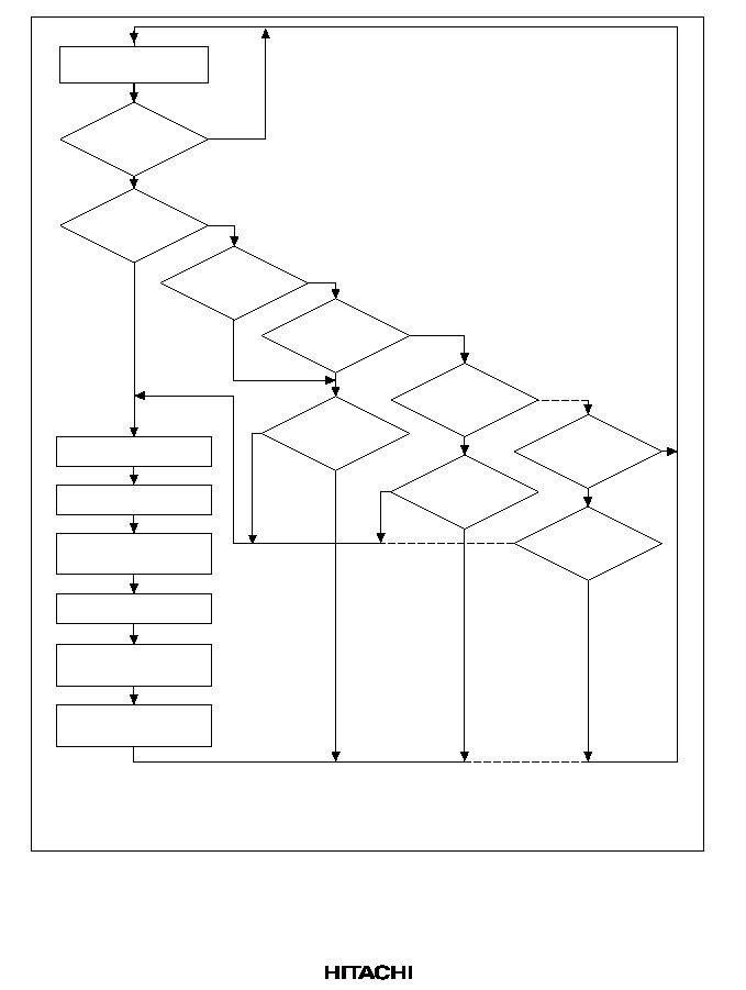
98
No
Yes
NMI?
No
Yes
User break?
No
Yes
Level 15
interrupt?
No
Yes
I3 to I0
level 14?
No
Yes
Level 14
interrupt?
No
Yes
Yes
I3 to I0
level 13?
No
Yes
Level 1
interrupt?
No
Yes
I3 to I0 =
level 0?
No
Program execution
state
Save SR to stack
Save PC to stack
Read vector number*
Branch to exception
service routine
Interrupt
generated?
Copy accepted
interrupt level to I3I0
Read exception
vector table
I3-I0:
Status register interrupt mask bits.
Note: The vector number is only read from an external source when an external
vector number is specified for the IRL interrupt vector number.
Figure 5.5 Interrupt Sequence Flowchart
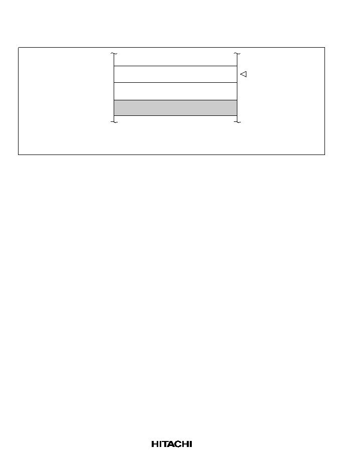
99
5.4.2
Stack after Interrupt Exception Handling
Figure 5.6 shows the stack after interrupt exception handling.
32 bits
32 bits
SR
PC*
Address
4n 8
4n 4
4n
SP
Note: PC: Start address of next instruction after the executing instruction (return destination
instruction)
Figure 5.6 Stack after Interrupt Exception Handling

100
5.5
Interrupt Response Time
Table 5.8 shows the interrupt response time, which is the time from the occurrence of an interrupt
request until interrupt exception handling starts and fetching of the first instruction of the interrupt
service routine begins. Figure 5.7 shows the pipeline when an IRL interrupt is accepted.
Table 5.8
Interrupt Response Time
Number of States
Item
NMI
Peripheral
Module
IRL
Notes
Compare identified inter-
rupt priority with SR mask
level
2
5
--
Wait for completion of
sequence currently being
executed by CPU
X (
0)
The longest sequence is
for interrupt or address-
error exception handling
(X = 4 + m1 + m2 + m3 +
m4). If an interrupt-
masking instruction
follows, however, the
time may be even longer.
Time from interrupt
exception handling (SR
and PC saves and vector
address fetch) until fetch
of first instruction of
exception service routine
starts
5 + m1 + m2 + m3
--
Interrupt
Total: 7 + m1 + m2 + m3
10 + m1 + m2 + m3
--
response
Minimum: 10
13
--
Maximum: 11 + 2 (m1 + m2 +
m3) + m4
14 + 2 (m1 + m2 +
m3) + m4
--
Note:
m1m4 are the number of states needed for the following memory accesses
m1: SR save (longword write)
m2: PC save (longword write)
m3: Vector address read (longword read)
m4: Fetch of first instruction of interrupt service routine
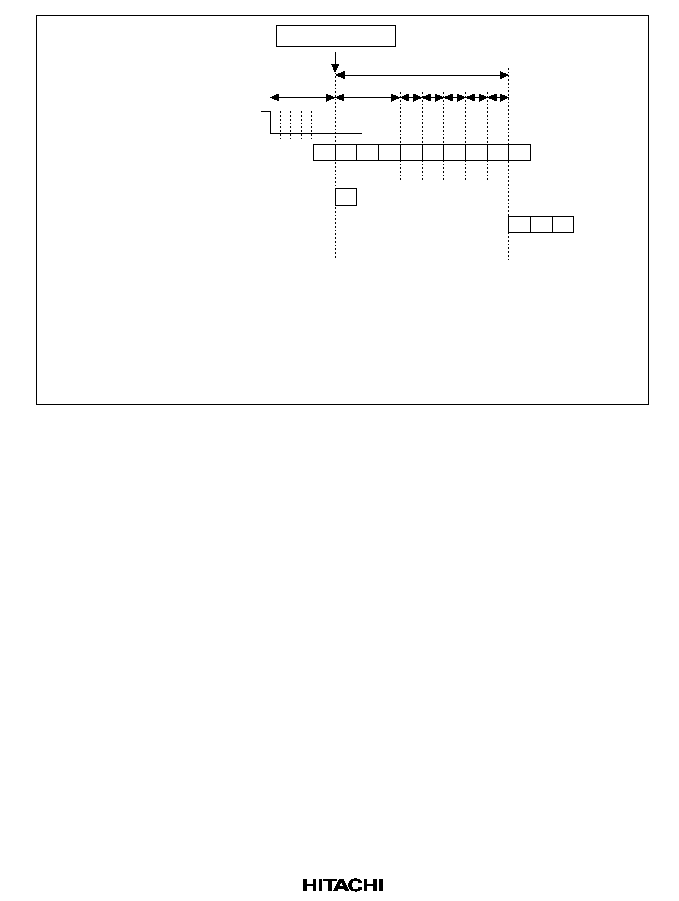
101
F
D E
M E
E
M M E
E
E
F
D
F
5
3
Interrupt accepted
IRL3
IRL0
m1 m2 1 m3 1
5 + m1 + m2 + m3
Instruction (instructions
replaced during interrupt
exception handling)
Overrun fetch
Interrupt service routine
start instruction
When m1 = m2 = m3 = 1, the
interrupt response time is 13 cycles
F:
Instruction fetch (instruction fetched from memory where program is stored)
D:
Instruction decoding (fetched instruction is decoded)
E:
Instruction execution (data operation and address calculation is performed
according to the results of decoding)
M:
Memory access (data in memory is accessed)
Figure 5.7 Pipeline when an IRL Interrupt is Accepted
5.6
Sampling of Pins
IRL3IRL0
Signals on interrupt pins
IRL3 to IRL0 pass through the noise canceler before being sent by the
interrupt controller to the CPU as interrupt requests. The noise canceler cancels noise that changes
in short cycles. The CPU samples the interrupt requests between executing instructions. During
this period, the noise canceler output changes according to the noise-eliminated pin level, so the
pin level must be held until the CPU samples it. This means that interrupt sources generally must
not be cleared inside interrupt routines.
When an external vector is fetched, the interrupt source can also be cleared when the external
vector fetch cycle is detected.
Figure 5.8 shows a block diagram of the interrupt response procedure. Figure 5.9 shows interrupt
response timing.
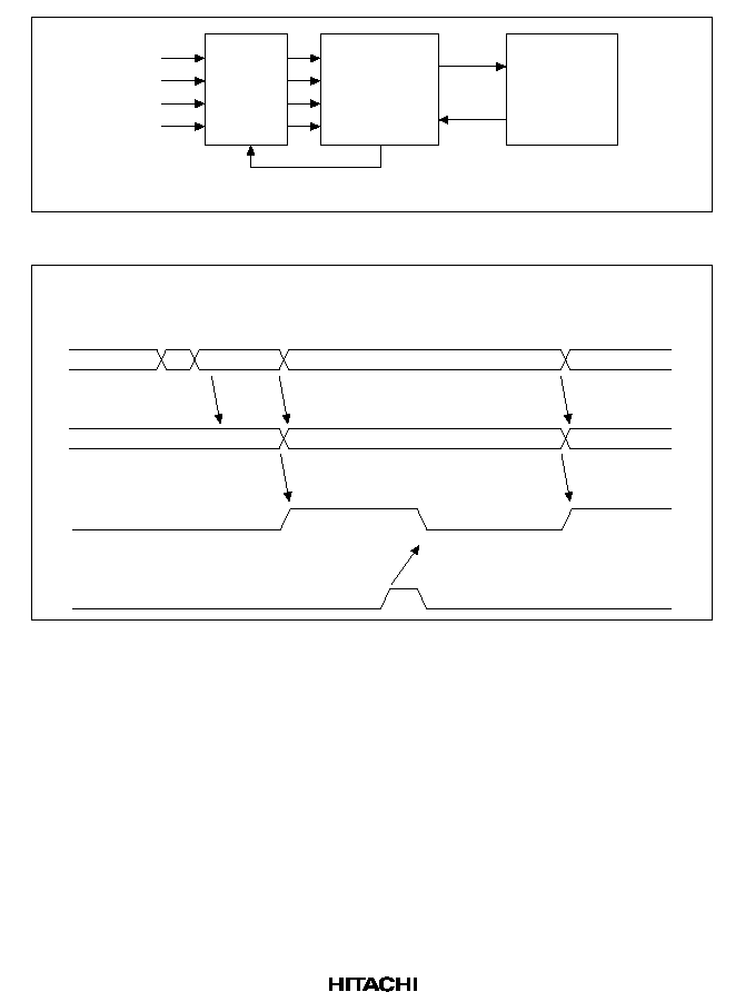
102
IRL0
IRL1
IRL2
IRL3
CPU
Interrupt
controller
Noise
canceler
Interrupt
request
Interrupt
accepted
Pin level cleared
when interrupt is accepted
Figure 5.8 Interrupt Response Block Diagram
Interrupt acceptance
signal to CPU
Interrupt request
to CPU
Noise canceler
output
Cleared when interrupt is accepted
IRL3
IRL0
pin level
1011 for
1 clock
due to
noise
Level 2 interrupt
Level 6 interrupt
1111
1111
1101
1001
1111
1101
1001
Figure 5.9 Interrupt Response Timing Chart
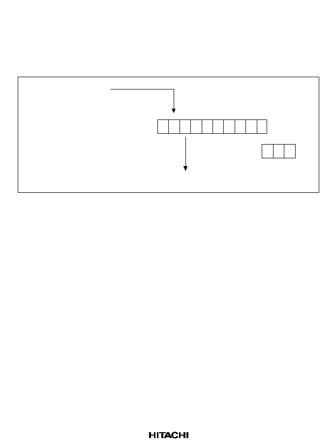
103
5.7
Usage Notes
1. Do not execute module standby for modules that have the module-stop function when the
possibility remains that an interrupt request may be output.
2. As shown in figure 5.10, the point at which the NMI request is cleared is the state following
the decoding stage for the instruction replaced by the interrupt exception handling.
F
D
E
E
M
M
E
M
E
E
F
D
E
NMI request
clearing timing
NMI request
(at fall)
Instruction replaced by
interrupt exception
handling
Start instruction in
NMI routine
Figure 5.10 NMI Request Clearing Timing
3. Clearing Interrupt Sources:
External Interrupt Sources: When an interrupt source is cleared by writing to an I/O address,
another instruction will be executed before the write can be completed because of the write
buffer. To ensure that the next instruction is executed after the write is completed, read from
the same address after the write to obtain total synchronization.
·
Returning from interrupt handling with an RTE instruction: Figure 5.11 shows how a
minimum interval of 1 cycle is required between the read instruction used for
synchronization and the RTE instruction. A read instruction for synchronization and a
minimum of 1 instruction should thus be executed between the source clear and the RTE
instruction.
·
Changing the level during interrupt handling: Figure 5.12 shows how a minimum interval
of 4 cycles is required between the synchronization instruction and the LDC instruction
when an LDC instruction is used to enable another overlapping interrupt by changing the
SR value. A read instruction for synchronization and a minimum of 4 instructions should
thus be executed between the source clear and the LDC instruction.
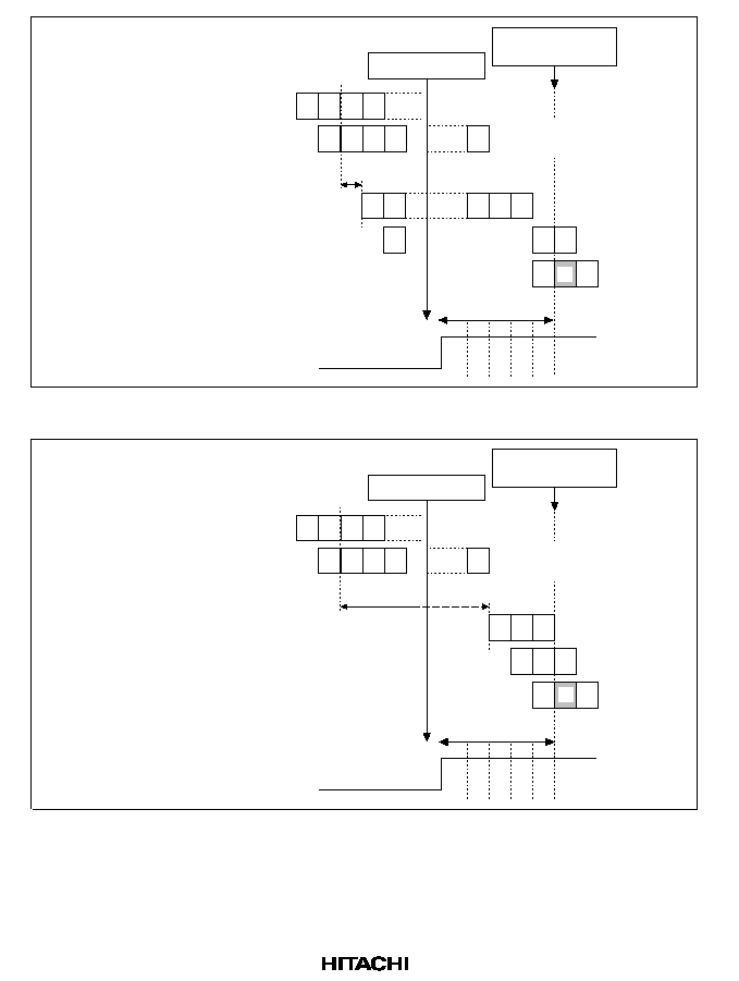
104
Writing complete
Next interrupt can
be accepted
M
E
D
D
F
F
ex. mov r0,@r1
Interrupt clear instruction
ex. mov @r1,r0
Synchronization instruction
RTE instruction
Delay slot instruction
Instruction at destination
of return from interrupt
IRL3
IRL0
External write
Min. 2 cycles
External read
Min. 2 cycles
M
1 cycle
W
E
D
F
F
M
D E
M
5 cycles
E
E
D
F
Figure 5.11 Pipeline Operation in Return with RTE
Writing complete
Next interrupt can
be accepted
M
E
D
D
F
F
ex. mov r0,@r1
Interrupt clear instruction
ex. mov @r1,r0
Synchronization instruction
LDC instruction
Interrupt-disable instruction
Ordinary instruction
IRL3
IRL0
External write
Min. 2 cycles
External read
Min. 2 cycles
M
4 cycles
W
E
F
E
D E
D
5 cycles
F
E
D
F
Figure 5.12 Pipeline Operation when Interrupts are Enabled by Modifying SR
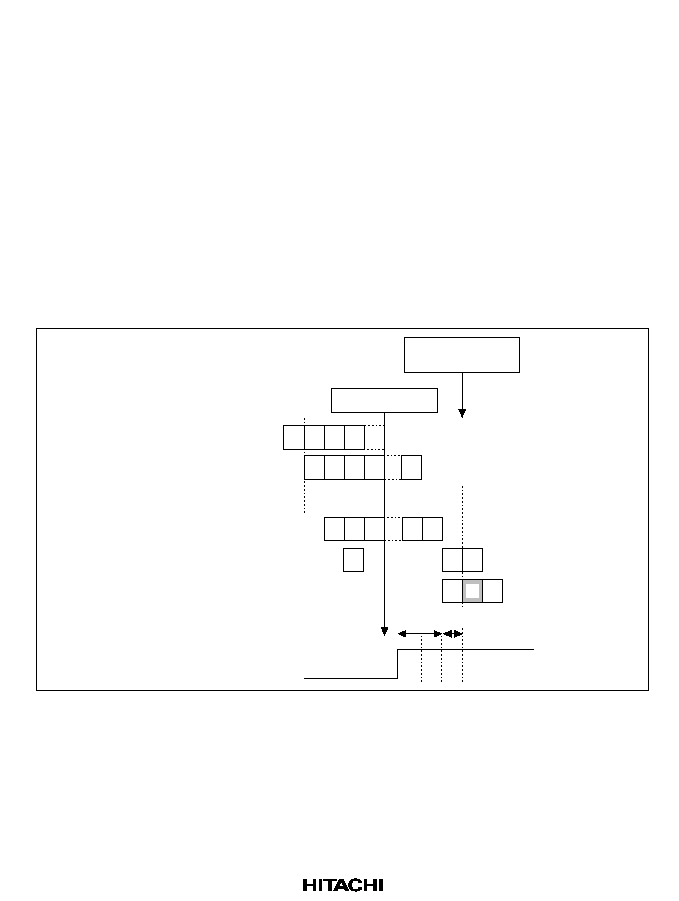
105
On-Chip Interrupt Sources: Pipeline operation must be taken into account to ensure that the
same interrupt does not occur again when the interrupt source is from an on-chip peripheral
module. At least 2 cycles are required for the CPU to recognize that the interrupt is from an on-
chip peripheral module. Two cycles are also required for the fact that there is no longer an
interrupt request to be relayed.
·
Returning from interrupt handling with an RTE instruction: Figure 5.13 shows how an extra
cycle is required after the read instruction used for synchronization before interrupts are
accepted, even when an RTE instruction is executed. A read instruction for synchronization
should thus be executed between the source clear and the RTE instruction.
·
Changing the level during interrupt handling: Figure 5.14 shows how a minimum interval of 2
cycles is required between the synchronization instruction and the LDC instruction when an
LDC instruction is used to enable another overlapping interrupt by changing the SR value. A
read instruction for synchronization and a minimum of 2 instructions should thus be executed
between the source clear and the LDC instruction.
Writing complete
Next interrupt can
be accepted
M
E
D
D
F
F
ex. mov r0,@r1
Interrupt clear instruction
ex. mov @r1,r0
Synchronization instruction
RET instruction
Delay slot instruction
Instruction at destination
of return from interrupt
On-chip peripheral interrupt
On-chip peripheral write
Min. 1 cycle
On-chip peripheral read
Min. 1 cycle
M
W
E
E
F
D
F
D E
2 cycles
M M
E
D
F
1-cycle margin
Figure 5.13 Pipeline Operation in Return with RTE
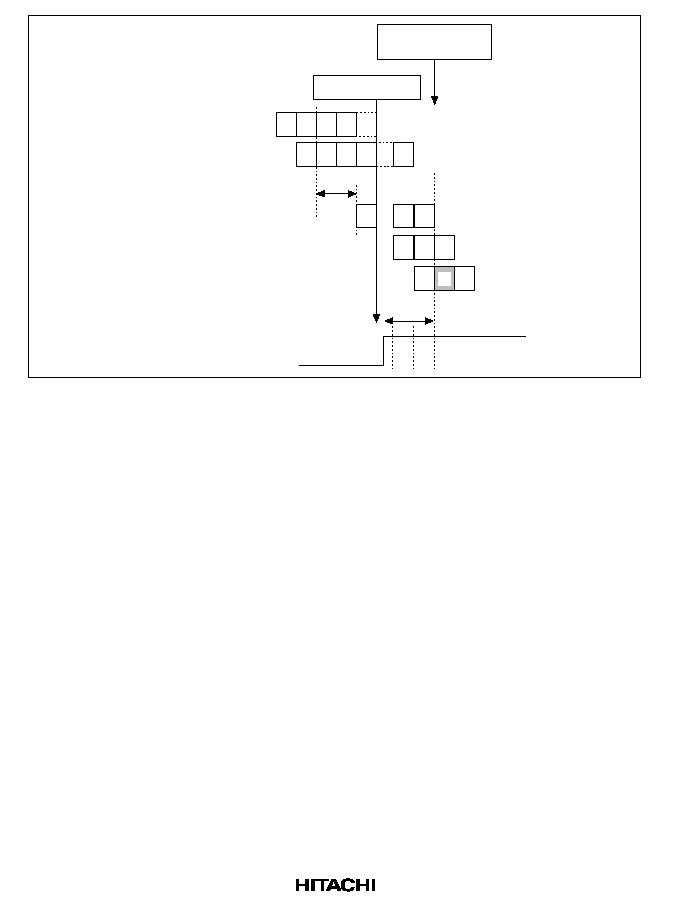
106
Writing complete
Next interrupt can
be accepted
M
E
D
D
F
F
ex. mov r0,@r1
Interrupt clear instruction
ex. mov @r1,r0
Synchronization instruction
LDC instruction
Interrupt-disable instruction
Ordinary instruction
On-chip peripheral interrupt
On-chip peripheral write
Min. 1 cycle
On-chip peripheral read
Min. 1 cycle
M
W
E
F
E
2 cycles
2 cycles
D E
F D
E
D
F
Figure 5.14 Pipeline Operation when Interrupts are Enabled by Changing the SR

107
Section 6 User Break Controller
6.1
Overview
The user break controller (UBC) provides functions that simplify program debugging. Break
conditions are set in the UBC and a user break interrupt is generated according to the conditions of
the bus cycle generated by the CPU, on-chip DMAC, or external bus master.
This function makes it easy to design an effective self-monitoring debugger, enabling the chip to
debug programs without using an in-circuit emulator. The UBC can be set in an SH7000 series
compatible mode, facilitating porting of monitoring programs that use other SH7000 series UBCs.
6.1.1
Features
The features of the user break controller are listed below:
·
The following break compare conditions can be set: Two break channels (channel A, channel
B). User break interrupts can be requested using either independent or sequential condition for
the two channels (sequential breaks are channel A, then channel B).
Address
Data (channel B only)
Bus master: CPU cycle/DMA cycle/external bus cycle
Bus cycle: instruction fetch/data access
Read or write
Operand size: byte/word/longword
·
User break interrupt generated upon satisfying break conditions. A user-designed user break
interrupt exception handling routine can be run.
·
Select breaking in the instruction fetch cycle before the instruction is executed, or after.
·
Compatible with SH7000 series UBCs after a power-on reset.
108
6.1.2
Block Diagram
BARAH
BARAL
BAMRAH
BBRA
BARBH
BARBL
BAMRBH BAMRBL
BDRBH
BDRBL
BDMRBH BDMRBL
BBRB
BRCR
Control
Channel B
Access
Data
Address
Channel A
Access
Address
Module data bus
Internal data bus
Cache data bus
Access
BAMRAL
Internal address bus
Internal interrupt signal
Cache address bus
BARAH/L:
Break address register AH/L
BAMRAH/L:
Break address mask register AH/L
BBRA:
Break bus cycle register A
BARBH/L:
Break address register BH/L
BAMRBH/L:
Break address mask register BH/L
BDRBH/L:
Break data register BH/L
BDMRBH/L: Break data mask register BH/L
BBRB:
Break bus cycle register B
BRCR:
Break control register
Figure 6.1 User Break Controller Block Diagram

109
6.1.3
Register Configuration
Table 6.1
Register Configuration
Name
Abbr.
R/W
Initial
Value*
1
Address
Access Size
*2
Break address register AH
BARAH
R/W
H'0000 H'FFFFFF40
16
32
Break address register AL
BARAL
R/W
H'0000 H'FFFFFF42
16
Break address mask register AH
BAMRAH
R/W
H'0000 H'FFFFFF44
16
32
Break address mask register AL
BAMRAL
R/W
H'0000 H'FFFFFF46
16
Break bus cycle register A
BBRA
R/W
H'0000 H'FFFFFF48
16, 32
Break address register BH
BARBH
R/W
H'0000 H'FFFFFF60
16
32
Break address register BL
BARBL
R/W
H'0000 H'FFFFFF62
16
Break address mask register BH
BAMRBH
R/W
H'0000 H'FFFFFF64
16
32
Break address mask register BL
BAMRBL
R/W
H'0000 H'FFFFFF66
16
Break data register BH
BDRBH
R/W
H'0000 H'FFFFFF70
16
32
Break data register BL
BDRBL
R/W
H'0000 H'FFFFFF72
16
Break data mask register BH
BDMRBH
R/W
H'0000 H'FFFFFF74
16
32
Break data mask register BL
BDMRBL
R/W
H'0000 H'FFFFFF76
16
Break bus cycle register B
BBRB
R/W
H'0000 H'FFFFFF68
16, 32
Break control register
BRCR
R/W
H'0000 H'FFFFFF78
16, 32
Notes: 1. Initialized by a power-on reset. Values held in standby mode. Value undefined after a
manual reset.
2. Byte access not permitted.
SH7000 Series UBC Compatibility: When set in the SH7000-series-compatible mode, SH7000
series UBC registers on the SH7604 are as shown in table 6.2.
Table 6.2
SH7000 Series and SH7604 UBCs
SH7000 Series
SH7604
Name
Abbr.
Name
Abbr.
Break address register H
BARH
Break address register AH
BARAH
Break address register L
BARL
Break address register AL
BARAL
Break address mask register H
BAMRH
Break address mask register AH
BAMRAH
Break address mask register L
BAMRL
Break address mask register AL
BAMRAL
Break bus cycle register
BBR
Break bus cycle register A
BBRA

110
6.2
Register Descriptions
6.2.1
Break Address Register A (BARA)
BARAH:
Bit:
15
14
13
12
11
10
9
8
Bit name:
BAA31
BAA30
BAA29
BAA28
BAA27
BAA26
BAA25
BAA24
Initial value:
0
0
0
0
0
0
0
0
R/W:
R/W
R/W
R/W
R/W
R/W
R/W
R/W
R/W
Bit:
7
6
5
4
3
2
1
0
Bit name:
BAA23
BAA22
BAA21
BAA20
BAA19
BAA18
BAA17
BAA16
Initial value:
0
0
0
0
0
0
0
0
R/W:
R/W
R/W
R/W
R/W
R/W
R/W
R/W
R/W
BARAL:
Bit:
15
14
13
12
11
10
9
8
Bit name:
BAA15
BAA14
BAA13
BAA12
BAA11
BA10
BAA9
BAA8
Initial value:
0
0
0
0
0
0
0
0
R/W:
R/W
R/W
R/W
R/W
R/W
R/W
R/W
R/W
Bit:
7
6
5
4
3
2
1
0
Bit name:
BAA7
BAA6
BAA5
BAA4
BAA3
BAA2
BAA1
BAA0
Initial value:
0
0
0
0
0
0
0
0
R/W:
R/W
R/W
R/W
R/W
R/W
R/W
R/W
R/W
The two break address registers A--break address register AH (BARAH) and break address
register AL (BARAL)--together form a single group. Both are 16-bit read/write registers.
BARAH stores the upper bits (bits 31 to 16) of the address of the channel A break condition, while
BARAL stores the lower bits (bits 15 to 0). A power-on reset initializes both BARAH and
BARAL to H'0000. Their values are undefined after a manual reset.
·
BARAH Bits 15 to 0--Break Address A 31 to 16 (BAA31 to BAA16): These bits store the
upper bit values (bits 31 to 16) of the address of the channel A break condition.
·
BARAL Bits 15 to 0--Break Address A 15 to 0 (BAA15 to BAA0): These bits store the lower
bit values (bits 15 to 0) of the address of the channel A break condition.
111
6.2.2
Break Address Mask Register A (BAMRA)
BAMRAH:
Bit:
15
14
13
12
11
10
9
8
Bit name: BAMA31 BAMA30 BAMA29 BAMA28 BAMA27 BAMA26 BAMA25 BAMA24
Initial value:
0
0
0
0
0
0
0
0
R/W:
R/W
R/W
R/W
R/W
R/W
R/W
R/W
R/W
Bit:
7
6
5
4
3
2
1
0
Bit name: BAMA23 BAMA22 BAMA21 BAMA20 BAMA19 BAMA18 BAMA17 BAMA16
Initial value:
0
0
0
0
0
0
0
0
R/W:
R/W
R/W
R/W
R/W
R/W
R/W
R/W
R/W
BAMRAL:
Bit:
15
14
13
12
11
10
9
8
Bit name: BAMA15 BAMA14 BAMA13 BAMA12 BAMA11 BAMA10 BAMA9
BAMA8
Initial value:
0
0
0
0
0
0
0
0
R/W:
R/W
R/W
R/W
R/W
R/W
R/W
R/W
R/W
Bit:
7
6
5
4
3
2
1
0
Bit name:
BAMA7
BAMA6
BAMA5
BAMA4
BAMA3
BAMA2
BAMA1
BAMA0
Initial value:
0
0
0
0
0
0
0
0
R/W:
R/W
R/W
R/W
R/W
R/W
R/W
R/W
R/W
The two break address mask registers A (BAMRA)--break address mask register AH
(BAMRAH) and break address mask register AL (BAMRAL)--together form a single group.
Both are 16-bit read/write registers. BAMRAH determines which of the bits in the break address
set in BARAH are masked. BAMRAL determines which of the bits in the break address set in
BARAL are masked. A power-on reset initializes BAMRAH and BAMRAL to H'0000. Their
values are undefined after a manual reset.
·
BAMRAH Bits 15 to 0--Break Address Mask A 31 to 16 (BAMA31 to BAMA16): These bits
specify whether bits 3116 (BAA31 to BAA16) of the channel A break address set in BARAH
are masked.
·
BAMRAL Bits 15 to 0--Break Address Mask A 15 to 0 (BAMA15 to BAMA0): These bits
specify whether bits 150 (BAA15 to BAA0) of the channel A break address set in BARAL
are masked.
112
Bits 31
0: BAMAn
Description
0
Channel A break address BAAn is included in the break conditions
(Initial value)
1
Channel A break address BAAn is masked and therefore not included
in the break conditions
n = 31 to 0
6.2.3
Break Bus Cycle Register A (BBRA)
Bit:
15
14
13
12
11
10
9
8
Bit name:
--
--
--
--
--
--
--
--
Initial value:
0
0
0
0
0
0
0
0
R/W:
R
R
R
R
R
R
R
R
Bit:
7
6
5
4
3
2
1
0
Bit name:
CPA1
CPA0
IDA1
IDA0
RWA1
RWA0
SZA1
SZA0
Initial value:
0
0
0
0
0
0
0
0
R/W:
R/W
R/W
R/W
R/W
R/W
R/W
R/W
R/W
The break bus cycle register A (BBRA) is a 16-bit read/write register that selects the following
four channel A break conditions:
1. CPU cycle/peripheral cycle
2. Instruction fetch/data access
3. Read/write
4. Operand size
A power-on reset initializes BBRA to H'0000. Its value is undefined after a manual reset.
·
Bits 15 to 8--Reserved: These bits always read 0. The write value should always be 0.
·
Bits 7 and 6--CPU Cycle/Peripheral Cycle Select A (CPA1, CPA0): These bits select whether
to break channel A on a CPU and/or peripheral bus cycle. Peripheral cycles are defined as on-
chip DMAC bus cycles, and external bus master bus cycles when the bus is released. When the
peripheral cycle setting is made, on-chip DMAC cycles are always included in the break
conditions; however, external bus master cycles can be included or excluded, according to the
setting of the EBBE bit in the BRCR register.

113
Bit 7: CPA1
Bit 6: CPA0
Description
0
0
No channel A user break interrupt occurs
(Initial value)
1
Break only on CPU cycles
1
0
Break only on peripheral cycles
1
Break on both CPU and peripheral cycles
·
Bits 5 and 4--Instruction Fetch/Data Access Select A (IDA1, IDA0): These bits select whether
to break channel A on instruction fetch and/or data access cycles.
Bit 5: IDA1
Bit 4: IDA0
Description
0
0
No channel A user break interrupt occurs
(Initial value)
1
Break only on instruction fetch cycles
1
0
Break only on data access cycles
1
Break on both instruction fetch and data access cycles
·
Bits 3 and 2--Read/Write Select A (RWA1, RWA0): These bits select whether to break
channel A on read and/or write cycles.
Bit 3: RWA1
Bit 2: RWA0
Description
0
0
No channel A user break interrupt occurs
(Initial value)
1
Break only on read cycles
1
0
Break only on write cycles
1
Break on both read and write cycles
·
Bits 1 and 0--Operand Size Select A (SZA1, SZA0): These bits select bus cycle operand size
as a channel A break condition.
Bit 1: SZA1
Bit 0: SZA0
Description
0
0
Operand size is not a break condition
(Initial value)
1
Break on byte access
1
0
Break on word access
1
Break on longword access
Note:
When breaking on an instruction fetch, set the SZA0 bit to 0. All instructions are considered
to be word-size accesses (instruction fetches are always longword). Operand size is word
for instructions or determined by the operand size specified for the CPU/DMAC data
access. It is not determined by the bus width of the space being accessed.

114
6.2.4
Break Address Register B (BARB)
The channel B break address register has the same bit configuration as BARA.
6.2.5
Break Address Mask Register B (BAMRB)
The channel B break address mask register has the same bit configuration as BAMRA.
6.2.6
Break Data Register B (BDRB)
BDRBH:
Bit:
15
14
13
12
11
10
9
8
Bit name:
BDB31
BDB30
BDB29
BDB28
BDB27
BDB26
BDB25
BDB24
Initial value:
0
0
0
0
0
0
0
0
R/W:
R/W
R/W
R/W
R/W
R/W
R/W
R/W
R/W
Bit:
7
6
5
4
3
2
1
0
Bit name:
BDB23
BDB22
BDB21
BDB20
BDB19
BDB18
BDB17
BDB16
Initial value:
0
0
0
0
0
0
0
0
R/W:
R/W
R/W
R/W
R/W
R/W
R/W
R/W
R/W
BDRBL:
Bit:
15
14
13
12
11
10
9
8
Bit name:
BDB15
BDB14
BDB13
BDB12
BDB11
BDB10
BDB9
BDB8
Initial value:
0
0
0
0
0
0
0
0
R/W:
R/W
R/W
R/W
R/W
R/W
R/W
R/W
R/W
Bit:
7
6
5
4
3
2
1
0
Bit name:
BDB7
BDB6
BDB5
BDB4
BDB3
BDB2
BDB1
BDB0
Initial value:
0
0
0
0
0
0
0
0
R/W:
R/W
R/W
R/W
R/W
R/W
R/W
R/W
R/W
The two break data registers B (BDRB)--break data register BH (BDRBH) and break data register
BL (BDRBL)--together form a single group. Both are 16-bit read/write registers. BDRBH
specifies the upper half (bits 3116) of the data that is the break condition for channel B, while
BDRBL specifies the lower half (bits 150). A power-on reset initializes BDRBH and BDRBL to
H'0000. Their values are undefined after a manual reset.

115
·
BDRBH Bits 15 to 0--Break Data B 31 to 16 (BDB31 to BDB16): These bits store the upper
half (bits 3116) of the data that is the break condition for break channel B.
·
BDRBL Bits 15 to 0--Break Data B 15 to 0 (BDB15 to BDB0): These bits store the lower half
(bits 150) of the data that is the break condition for break channel B.
6.2.7
Break Data Mask Register B (BDMRB)
BDMRBH:
Bit:
15
14
13
12
11
10
9
8
Bit name: BDMB31 BDMB30 BDMB29 BDMB28 BDMB27 BDMB26 BDMB25 BDMB24
Initial value:
0
0
0
0
0
0
0
0
R/W:
R/W
R/W
R/W
R/W
R/W
R/W
R/W
R/W
Bit:
7
6
5
4
3
2
1
0
Bit name: BDMB23 BDMB22 BDMB21 BDMB20 BDMB19 BDMB18 BDMB17 BDMB16
Initial value:
0
0
0
0
0
0
0
0
R/W:
R/W
R/W
R/W
R/W
R/W
R/W
R/W
R/W
BDMRBL:
Bit:
15
14
13
12
11
10
9
8
Bit name: BDMB15 BDMB14 BDMB13 BDMB12 BDMB11 BDMB10 BDMB9 BDMB8
Initial value:
0
0
0
0
0
0
0
0
R/W:
R/W
R/W
R/W
R/W
R/W
R/W
R/W
R/W
Bit:
7
6
5
4
3
2
1
0
Bit name:
BDMB7
BDMB6 BDMB5
BDMB4 BDMB3
BDMB2
BDMB1 BDMB0
Initial value:
0
0
0
0
0
0
0
0
R/W:
R/W
R/W
R/W
R/W
R/W
R/W
R/W
R/W
The two break data mask registers B (BDMRB)--break data mask register BH (BDMRBH) and
break data mask register BL (BDMRBL)--together form a single group. Both are 16-bit
read/write registers. BDMRBH determines which of the bits in the break address set in BDRBH
are masked. BDMRBL determines which of the bits in the break address set in BDRBL are
masked. A power-on reset initializes BDMRBH and BDMRBL to H'0000. Their values are
undefined after a manual reset.
116
·
BDMRBH Bits 15 to 0--Break Data Mask B 31 to 16 (BDMB31 to BDMB16): These bits
specify whether bits B 3116 (BDB31 to BDB16) of the channel B break data set in BDRBH
are masked.
·
BDMRBL Bits 15 to 0--Break Data Mask B 15 to 0 (BDMB15 to BDMB0): These bits
specify whether bits B 150 (BDB15 to BDB0) of the channel B break data set in BDRBL are
masked.
Bits 31
0: BDMBn
Description
0
Channel B break address bit BDBn is included in the break condition
(Initial value)
1
Channel B break address bit BDBn is masked and therefore not
included in the break condition
n = 31 to 0
Notes: 1. When the data bus value is included in the break conditions, specify the operand size.
2. For word data, set in bits 150 of BDRB and BDMRB. For byte data, set the same data
in bits 07 and bits 815 of BDRB and BDMRB.
3. External bus master bus cycles when the bus is released cannot be included in the data
bus conditions.
6.2.8
Bus Break Register B (BBRB)
The channel B bus break register has the same bit configuration as BBRA.
6.2.9
Break Control Register (BRCR)
Bit:
15
14
13
12
11
10
9
8
Bit name:
CMFCA CMFPA
EBBE
UMD
--
PCBA
--
--
Initial value:
0
0
0
0
0
0
0
0
R/W:
R/W
R/W
R/W
R/W
R
R/W
R
R
Bit:
7
6
5
4
3
2
1
0
Bit name:
CMFCB CMFPB
--
SEQ
DBEB
PCBB
--
--
Initial value:
0
0
0
0
0
0
0
0
R/W:
R/W
R/W
R
R/W
R
R/W
R
R

117
The BRCR register:
1. Determines whether to use channels A and B as two independent channels or as sequential
conditions.
2. Selects SH7000 series compatible mode or SH7604 mode.
3. Selects whether to break before or after instruction execution during the instruction fetch cycle.
4. Enables or disables the external bus.
5. Selects whether to include the data bus in channel B comparison conditions.
It also has a condition-match flag that is set when conditions match. A power-on reset initializes
BRCR to H'0000. Its value is undefined after a manual reset.
·
Bit 15--CPU Condition-Match Flag A (CMFCA): Set to 1 when CPU bus cycle conditions
included in the break conditions set for channel A are met. Not cleared to 0.
Bit 15: CMFCA
Description
0
Channel A CPU cycle conditions do not match, no user break interrupt
generated
(Initial value)
1
Channel A CPU cycle conditions have matched, user break interrupt
generated
·
Bit 14--Peripheral Condition-Match Flag A (CMFPA): Set to 1 when peripheral bus cycle
conditions (on-chip DMAC, or external bus cycle when external bus breaks are enabled)
included in the break conditions set for channel A are met. Not cleared to 0.
Bit 14: CMFPA
Description
0
Channel A peripheral cycle conditions do not match, no user break
interrupt generated
(Initial value)
1
Channel A peripheral cycle conditions have matched, user break
interrupt generated
·
Bit 13--External Bus Break Enable (EBBE): Monitors the external bus master's address bus
when the bus is released, and includes the external bus master's bus cycle in the bus cycle
select conditions (CPA1, CPB1). External bus breaks are possible in the total master mode and
total slave mode. When the external bus break is enabled, set CPA1 in BBRA or CPB1 in
BBRB.
Bit 13: EBBE
Description
0
Chip-external bus cycle not included in break conditions
(Initial value)
1
Chip-external bus cycle included in break conditions

118
·
Bit 12--UBC Mode (UMD): Selects SH7000 series-compatible mode or SH7604 mode.
Bit 12: UMD
Description
0
Compatible mode for SH7000 Series UBCs
(Initial value)
1
SH7604 mode
·
Bit 11--Reserved: This bit always reads 0. The write value should always be 0.
·
Bit 10--PC Break Select A (PCBA): Selects whether to place the channel A break in the
instruction fetch cycle before or after instruction execution.
Bit 10: PCBA
Description
0
Places the channel A instruction fetch cycle break before instruction
execution
(Initial value)
1
Places the channel A instruction fetch cycle break after instruction
execution
·
Bits 9 and 8--Reserved: These bits always read 0. The write value should always be 0.
·
Bit 7--CPU Condition-Match Flag B (CMFCB): Set to 1 when CPU bus cycle conditions
included in the break conditions set for channel B are met. Not cleared to 0 (once set, it must
be cleared by a write before it can be used again).
Bit 7: CMFCB
Description
0
Channel B CPU cycle conditions do not match, no user break interrupt
generated
(Initial value)
1
Channel B CPU cycle conditions have matched, user break interrupt
generated
·
Bit 6--Peripheral Condition-Match Flag B (CMFPB): Set to 1 when peripheral bus cycle
conditions (on-chip DMAC, or external bus cycle when external bus monitoring is enabled)
included in the break conditions set for channel B are met. Not cleared to 0 (once set, it must
be cleared by a write before it can be used again).
Bit 6: CMFPB
Description
0
Channel B peripheral cycle conditions do not match, no user break
interrupt generated
(Initial value)
1
Channel B peripheral cycle conditions have matched, user break
interrupt generated

119
·
Bit 5--Reserved: This bit always reads 0. The write value should always be 0.
·
Bit 4--Sequence Condition Select (SEQ): Selects whether to handle the channel A and B
conditions independently or sequentially.
Bit 4: SEQ
Description
0
Channel A and B conditions compared independently
(Initial value)
1
Channel A and B conditions compared sequentially (channel A, then
channel B)
·
Bit 3--Data Break Enable B (DBEB): Selects whether to include data bus conditions in the
channel B break conditions.
Bit 3: DBEB
Description
0
Data bus conditions not included in the channel B conditions
(Initial value)
1
Data bus conditions included in the channel B conditions
·
Bit 2--Instruction Break Select (PCBB): Selects whether to place the channel B instruction
fetch cycle break before or after instruction execution.
Bit 2: PCBB
Description
0
Places the channel B instruction fetch cycle break before instruction
execution
(Initial value)
1
Places the channel B instruction fetch cycle break after instruction
execution
·
Bits 1 and 0--Reserved: These bits always read 0. The write value should always be 0.

120
6.3
Operation
6.3.1
Flow of the User Break Operation
The flow from setting of break conditions to user break interrupt exception handling is described
below:
1. The break addresses are set in the break address registers (BARA, BARB), the masked
addresses are set in the break address mask registers (BAMRA, BAMRB), the break data is set
in the break data register (BDRB), and the masked data is set in the break data mask register
(BDMRB). The breaking bus conditions are set in the break bus cycle registers (BBRA,
BBRB). The three groups of the BBRA and BBRB registers--CPU cycle/peripheral cycle
select, instruction fetch/data access select, and read/write select-- are each set. No user break
interrupt will be generated if even one of these groups is set with 00. The conditions are set in
the respective bits of the BRCR register.
2. When the set conditions are satisfied, the UBC sends a user break interrupt request to the
interrupt controller. When conditions match, the CPU condition match flags (CMFCA,
CMFCB) and peripheral condition match flags (CMFPA, CMFPB) for the respective channels
are set.
3. The interrupt controller checks the user break interrupt's priority level. The user break
interrupt has priority level 15, so it is accepted only if the interrupt mask level in bits I3I0 in
the status register (SR) is 14 or lower. When the I3I0 bit level is 15, the user break interrupt
cannot be accepted but it is held pending until user break interrupt exception handling can be
carried out. Section 5, Interrupt Controller, describes the handling of priority levels in greater
detail.
4. When the priority is found to permit acceptance of the user break interrupt, the CPU starts user
break interrupt exception handling.
5. The appropriate condition match flag (CMFCA, CMFPA, CMFCB, CMFPB) can be used to
check if the set conditions match or not. The flags are set by the matching of the conditions,
but they are not reset. 0 must first be written to them before they can be used again.
6.3.2
Break on Instruction Fetch Cycle
1. When CPU/instruction fetch/read/word is set in the break bus cycle registers (BBRA/BBRB),
the break condition becomes the CPU's instruction fetch cycle. Whether it breaks before or
after the execution of the instruction can then be selected for the appropriate channel with the
PCBA/PCBB bit in the break control register (BRCR).
2. The instruction fetch cycle always fetches 32 bits (two instructions). Only one bus cycle
occurs, but breaks can be placed on each instruction individually by setting the respective
addresses in the break address registers (BARA, BARB).

121
3. An instruction set for a break before execution breaks when it is confirmed that the instruction
has been fetched and will be executed. This means this feature cannot be used on instructions
fetched by overrun (instructions fetched at a branch or during an interrupt transition, but not to
be executed). When this kind of break is set for the delay slot of a delayed branch instruction
or an instruction following an interrupt-disabled instruction, such as LDC, the interrupt is
generated prior to execution of the first instruction at which the interrupt is subsequently then
accepted.
4. When the condition stipulates after execution, the instruction set with the break condition is
executed and then the interrupt is generated prior to the execution of the next instruction. As
with pre-execution breaks, this cannot be used with overrun fetch instructions. When this kind
of break is set for a delayed branch instruction or an interrupt-disabled instruction, such as
LDC, the interrupt is generated at the first instruction at which the interrupt is subsequently
accepted.
5. When an instruction fetch cycle is set for channel B, break data register B (BDRB) is ignored.
There is thus no need to set break data for an instruction fetch cycle break.
6.3.3
Break on Data Access Cycle
1. The memory cycles in which CPU data access breaks occur are: memory cycles from
instructions, and stacking and vector reads during exception handling. These breaks cannot be
used in dummy cycles for single reads of synchronous DRAM.
2. The relationship between the data access cycle address and the comparison condition for
operand size are shown in table 6.3. This means that when address H'00001003 is set without
specifying the size condition, for example, the bus cycle in which the break condition is
satisfied is as follows (where other conditions are met):
Longword access at address H'00001000
Word access at address H'00001002
Byte access at address H'00001003
Table 6.3
Data Access Cycle Addresses and Operand Size Comparison Conditions
Access Size
Address Compared
Longword
Break address register bits 312 compared with address bus bits 312
Word
Break address register bits 311 compared with address bus bits 311
Byte
Break address register bits 310 compared with address bus bits 310
3. When the data value is included in the break conditions on channel B:
When the data value is included in the break conditions, specify either longword, word, or byte
as the operand size in the break bus cycle registers (BBRA, BBRB). When data values are
included in break conditions, a break interrupt is generated when the address conditions and
data conditions both match. To specify byte data for this case, set the same data in the two

122
bytes at bits 158 and bits 70 of the break data register B (BDRB) and break data mask
register B (BDMRB). When word or byte is set, bits 3116 of BDRB and BDMRB are
ignored.
6.3.4
Break on External Bus Cycle
1. Enable the external bus break enable bit (the EBBE bit in BRCR) to generate a break for a bus
cycle generated by the external bus master when the bus is released. External bus cycle breaks
can be used in total master mode or total slave mode.
2. Address and read/write can be set for external buses, but size cannot be specified. Setting sizes
of byte/word/longword will be ignored. Also, no distinction can be made between instruction
fetch and data access for external bus cycles. All cycles are considered data access cycles, so
set 1 in bits IDA1 and IDB1 in BBRA and BBRB.
3. External input of addresses uses A26A0, so set bits 3127 of the break address registers
(BARA, BARB) to 0, or set bits 3127 of the break address mask registers (BAMRA,
BAMRB) to 1 to mask the addresses not input.
4. When the conditions set for the external bus cycle are satisfied, the CMFPA and CMFPB bits
are set for the respective channels.
6.3.5
Program Counter (PC) Values Saved
1. Break on Instruction Fetch (Before Execution): The program counter (PC) value saved to the
stack in user break interrupt exception handling is the address that matches the break condition.
The user break interrupt is generated before the fetched instruction is executed. If a break
condition is set on an instruction that follows an interrupt-disabled instruction, however, the
break occurs before execution of the instruction at which the next interrupt is accepted, so the
PC value saved is the address of the break.
2. Break on Instruction Fetch (After Execution): The program counter (PC) value saved to the
stack in user break interrupt exception handling is the address executed after the one that
matches the break condition. The fetched instruction is executed and the user break interrupt
generated before the next instruction is executed. If a break condition is set on an interrupt-
disabled instruction, the break occurs before execution of the instruction at which the next
interrupt is accepted, so the PC value saved is the address of the break.
3. Break on Data Access (CPU/Peripheral): The program counter (PC) value is the start address
of the next instruction after the last instruction executed before the user break exception
handling started. When data access (CPU/peripheral) is set as a break condition, the place
where the break will occur cannot be specified exactly. The break will occur at an instruction
fetched close to where the data access that is to receive the break occurs.

123
6.3.6
Example of Use
Break on a CPU Instruction Fetch Bus Cycle:
A.
Register settings:
BARA = H'00000404, BAMRA = H'00000000, BBRA = H'0054
BARB = H'00008010, BAMRB = H'00000006, BBRB = H'0054
BDRB = H'00000000, BDMRB = H'00000000
BRCR = H'1400
Conditions set (channel A/channel B independent mode):
Channel A:
Address = H'00000404, address mask H'00000000
Bus cycle = CPU, instruction fetch (after execution), read
(operand size not included in conditions)
Channel B:
Address = H'00008010, address mask H'00000006
Data H'00000000, data mask H'00000000
Bus cycle = CPU, instruction fetch (before execution), read
(operand size not included in conditions)
A user break will occur after the instruction at address H'00000404 is executed, or a user break
will be generated before the execution of the instruction at address H'00008010H'00008016.
B.
Register settings:
BARA = H'00037226, BAMRA = H'00000000, BBRA = H'0056
BARB = H'0003722E, BAMRB = H'00000000, BBRB = H'0056
BDRB = H'00000000, BDMRB = H'00000000
BRCR = H'1010
Conditions set (channel A
channel B sequential mode):
Channel A:
Address = H'00037226, address mask H'00000000
Bus cycle = CPU, instruction fetch (before execution), read, word
Channel B:
Address = H'0003722E, address mask H'00000000
Data H'00000000, data mask H'00000000
Bus cycle = CPU, instruction fetch (before execution), read, word
The instruction at address H'00037226 will be executed and then a user break interrupt will occur
before the instruction at address H'0003722E is executed.

124
C.
Register settings:
BARA = H'00027128, BAMRA = H'00000000, BBRA = H'005A
BARB = H'00031415, BAMRB = H'00000000, BBRB = H'0054
BDRB = H'00000000, BDMRB = H'00000000
BRCR = H'1000
Conditions set (channel A/channel B independent mode):
Channel A:
Address = H'00027128, address mask H'00000000
Bus cycle = CPU, instruction fetch (before execution), write , word
Channel B:
Address = H'00031415, address mask H'00000000
Data H'00000000, data mask H'00000000
Bus cycle = CPU, instruction fetch (before execution), read
(operand size not included in conditions)
A user break interrupt is not generated for channel A since the instruction fetch is not a write
cycle. A user break interrupt is not generated for channel B because the instruction fetch is for an
odd address.
D.
Register settings:
BARA = H'00037226, BAMRA = H'00000000, BBRA = H'005A
BARB = H'0003722E, BAMRB = H'00000000, BBRB = H'0056
BDRB = H'00000000, BDMRB = H'00000000
BRCR = H'1010
Conditions set (channel A
channel B sequential mode):
Channel A:
Address = H'00037226, address mask H'00000000
Bus cycle = CPU, instruction fetch (before execution), write, word
Channel B:
Address = H'0003722E, address mask H'00000000
Data H'00000000
Data mask H'00000000
Bus cycle = CPU, instruction fetch (before execution), read, word
The break for channel A is a write cycle, so conditions are not satisfied; since the sequence
conditions are not met, no user break interrupt occurs.

125
Break on CPU Data Access Cycle:
Register settings:
BARA = H'00123456, BAMRA = H'00000000, BBRA = H'0064
BARB = H'000ABCDE, BAMRB = H'000000FF, BBRB = H'006A
BDRB = H'0000A512, BDMRB = H'00000000
BRCR = H'1008
Conditions set (channel A/channel B independent mode):
Channel A:
Address = H'00123456, address mask H'00000000
Bus cycle = CPU, data access, read
(operand size not included in conditions)
Channel B:
Address = H'000ABCDE, address mask H'000000FF
Data H'0000A512, data mask H'00000000
Bus cycle = CPU, data access, write, word
For channel A, a user break interrupt occurs when it is read as longword at address H'00123454, as
word at address H'00123456 or as byte at address H'00123456. For channel B, a user break
interrupt occurs when H'A512 is written as word at H'000ABC00H'000ABCFE.
Break on DMAC Data Access Cycle:
Register settings:
BARA = H'00314156, BAMRA = H'00000000, BBRA = H'0094
BARB = H'00055555, BAMRB = H'00000000, BBRB = H'00A9
BDRB = H'00007878, BDMRB = H'00000F0F
BRCR = H'1008
Conditions set (channel A/channel B independent mode):
Channel A:
Address = H'00314156, address mask H'00000000
Bus cycle = DMA, instruction fetch, read
(operand size not included in conditions)
Channel B:
Address = H'00055555, address mask H'00000000
Data H'00007878, data mask H'00000F0F
Bus cycle = peripheral, data access, write, byte
For channel A, a user break interrupt does not occur, since no instruction fetch occurs in the
DMAC cycle. For channel B, a user break interrupt occurs when the DMAC writes H'7* (where *
means don't care) as byte at H'00055555.

126
6.3.7
Usage Notes
1. UBC registers can only be read or written to by the CPU.
2. When set for a sequential break, conditions match when a match of channel B conditions
occurs some time after the bus cycle in which a channel A match occurs. This means that the
conditions will not be satisfied when set for a bus cycle in which channel A and channel B
occur simultaneously. Since the CPU uses a pipeline structure, the order of the instruction
fetch cycle and memory cycle is fixed, so sequential conditions will be satisfied when the
respective channel conditions are met in the order the bus cycles occur.
3. When set for sequential conditions (the SEQ bit in BRCR is 1) and the instruction fetch cycle
of the channel A CPU is set as a condition, set channel A for before instruction execution
(PCBA bit in BRCR is 0).
4. When register settings are changed, the write values usually become valid after three cycles.
For on-chip memory, instruction fetches get two instructions simultaneously. If a break
condition is set on the fetch of the second of these two instructions but the contents of the UBC
registers are changed so as to alter the break condition immediately after the first of the two
instructions is fetched, a user break interrupt will still occur before the second instruction. To
ensure the timing of the change in the setting, read the register written last as a dummy. The
changed settings will be valid thereafter.
5. When a user break interrupt is generated upon a match of the instruction fetch condition and
the conditions match again in the UBC while the exception handling service routine is
executing, the break will cause exception handling when the I3I0 bits in SR are set to 14 or
lower. When masking addresses, when setting instruction fetch and after-execution as break
conditions, and when executing in steps, the UBC's exception service routine should not cause
a match of addresses with the UBC.
6. When the emulator is used, the UBC is used on the emulator system side to implement the
emulator's break function. This means none of the UBC functions can be used when the
emulator is being used.

127
6.3.8
SH7000 Series Compatible Mode
1. In SH7000 Series compatible mode:
In SH7000 Series compatible mode, functions are as follows:
·
The registers shown in the table 6.2 are valid; all others are not.
·
External bus breaks are not possible in SH7000 Series compatible mode. The instruction fetch
cycle occurs prior to instruction execution. The flags are not set when break conditions match.
2. Differences between SH7000 Series compatible mode and SH7604 mode:
When set for the CPU instruction fetch cycle in the SH7000 Series compatible mode, the break
occurs before the instruction that matches the conditions. The break conditions differ as shown
below from setting for before-execution in SH7604 mode. For data access cycles, the address
is always compared to 32 bits in the SH7000 Series compatible mode, but in SH7604 mode is
compared as shown in table 6.3. This produces the differences in break conditions shown in
table 6.4.
Table 6.4
Differences in Break Conditions
Match Determination
SH7000 Series
Compatible Mode
SH7604 Mode
Conditions match when set for instruction
fetch cycle/before-execution
Breaks if instruction is
overrun-fetched and
not executed (as during
branching)
Does not break if
instruction is overrun
fetched and not executed
(as during branching)
Conditions match in longword access when
set for addresses other than longword
boundaries (4n address)
Does not break
Breaks
Conditions match in word access when set
for addresses other than word boundaries
(2n addresses)
Does not break
Breaks

128

129
Section 7 Bus State Controller (BSC)
7.1
Overview
The bus state controller (BSC) manages the address spaces and outputs control signals so that
optimum memory accesses can be made in the four spaces. This enables memories like DRAM,
synchronous DRAM and pseudo-SRAM, and peripheral chips, to be linked directly.
7.1.1
Features
The BSC has the following features:
·
Address space is divided into four spaces
A maximum linear 32 Mbytes for each of the address spaces CS0CS3
The type of memory connected can be specified for each space (DRAM, synchronous
DRAM, pseudo-SRAM, burst ROM, etc.).
Bus width can be selected for each space (8, 16, or 32 bits).
Wait state insertion can be controlled for each space.
Outputs control signals for each space.
·
Cache
Cache areas and cache-through areas can be selected by access address.
When a cache access misses, 16 bytes are read consecutively in 4-byte units (because of
cache fill); writes use the write-through system.
Cache-through accesses are accessed according to access size.
·
Refresh
Supports CAS-before-RAS refresh (auto-refresh) and self-refresh.
Refresh interval can be set using the refresh counter and clock selection.
·
Direct interface to DRAM
Multiplexes row/column address output.
Burst transfer during reads, high-speed page mode for consecutive accesses.
Generates a Tp cycle to ensure RAS precharge time.
·
Direct interface to synchronous DRAM
Multiplexes row/column address output.
Burst read, single write
Bank active mode

130
·
Master and slave modes (bus arbitration)
Total master and partial-share master modes. In total master mode, all resources are shared
with other CPUs. Bus permission is shared when an external bus release request is
received. In partial-share master mode, only the CS2 space is shared with other CPUs; all
other spaces can be accessed at any time.
In slave mode, the external bus is accessed when a bus use request is output and bus use
permission is received.
·
Refresh counter can be used as an interval timer
Interrupt request generated upon compare match (CMI interrupt request signal).
7.1.2
Block Diagram
Figure 7.1 shows the BSC block diagram.
131
BCR1
BCR2
Area
control
unit
MCR
BSC
RTCSR
RTCNT
RTCOR
Comparator
Memory
control
unit
WCR
Wait
control
unit
WAIT
CS3
CS0
BS
RD
CAS
RAS
RD/
WR
WE3
WE0
CKE
IVECF
Interrupt
controller
Peripheral bus
Module bus
Internal bus
Bus
interface
CMI interrupt request
WCR: Wait control register
RTCNT: Refresh timer counter
BCR: Bus control register
RTCOR: Refresh time constant register
MCR: Individual memory control register
RTCSR: Refresh timer control/status register
Figure 7.1 BSC Block Diagram

132
7.1.3
Pin Configuration
Table 7.1 lists the bus state controller pin configuration.
Table 7.1
Pin Configuration
Signal
I/O
With Bus
Released
Description
A26A0
I/O
I
Address bus. 27 bits are available to specify a total 128 Mbytes of
memory space. The most significant 2 bits are used to specify the
CS space, so the size of the spaces is 32 Mbytes. When the bus is
released, these become inputs for the external bus cycle address
monitor.
D31D0
I/O
Hi-Z
32-bit data bus. When reading or writing a 16-bit width area, use
D15D0; when reading or writing a 8-bit width area, use D7D0.
With 8-bit accesses that read or write a 32-bit width area, input and
output the data via the byte position determined by the lower
address bits of the 32-bit bus.
BS
I/O
I
Indicates start of bus cycle or monitor. With the basic interface
(device interfaces except for DRAM, synchronous DRAM, pseudo-
SRAM), signal is asserted for a single clock cycle simultaneous
with address output. The start of the bus cycle can be determined
by this signal. This signal is asserted for 1 cycle synchronous with
column address output in DRAM, synchronous DRAM and pseudo-
SRAM accesses. When the bus is released,
BS
becomes an input
for address monitoring of external bus cycles.
CS0
CS3
O
Hi-Z
Chip select. Signals that select area; specified by A26 and A25.
RD/
WR
,
WE
I/O
I
Read/write signal. Signal that indicates access cycle direction
(read/write). Connected to
WE
pin when DRAM/synchronous
DRAM is connected. When the bus is released, becomes an input
for address monitoring of external bus cycles.
RAS
,
CE
O
Hi-Z
RAS
pin for DRAM/synchronous DRAM.
CE
pin for pseudo-SRAM.
CAS
,
OE
O
Hi-Z
Open when using DRAM.
CAS
pin for synchronous DRAM.
OE
pin
for pseudo-SRAM.
CASHH
,
DQMUU,
WE3
O
Hi-Z
When DRAM is used, connected to
CAS
pin for the most
significant byte (D31D24). When synchronous DRAM is used,
connected to DQM pin for the most significant byte. When pseudo-
SRAM is used, connected to
WE
pin for the most significant byte.
For basic interface, indicates writing to the most significant byte.
CASHL
,
DQMUL,
WE2
O
Hi-Z
When DRAM is used, connected to
CAS
pin for the second byte
(D23D16). When synchronous DRAM is used, connected to DQM
pin for the second byte. When pseudo-SRAM is used, connected
to
WE
pin for the second byte. For basic interface, indicates writing
to the second byte.

133
Table 7.1
Pin Configuration (cont)
Signal
I/O
With Bus
Released
Description
CASLH
,
DQMLU,
WE1
O
Hi-Z
When DRAM is used, connected to
CAS
pin for the third byte
(D15D8). When synchronous DRAM is used, connected to DQM
pin for the third byte. When pseudo-SRAM is used, connected to
WE
pin for the third byte. For basic interface, indicates writing to
the third byte.
CASLL
,
DQMLL,
WE0
O
Hi-Z
When DRAM is used, connected to
CAS
pin for the least significant
byte (D7D0). When synchronous DRAM is used, connected to
DQM pin for the least significant byte. When pseudo-SRAM is
used, connected to
WE
pin for the least significant byte. For basic
interface, indicates writing to the least significant byte.
RD
O
Hi-Z
Read pulse signal (read data output enable signal). Normally,
connected to the device's /OE pin; when there is an external data
buffer, the read cycle data can only be output when this signal is
low.
WAIT
I
Ignore
Hardware wait input.
BACK
,
BRLS
I
I
Bus use enable input in partial-share master or slave mode:
BACK
.
Bus release request input in total master:
BRLS
.
BREQ
,
BGR
O
O
Bus request output in partial-share master or slave mode:
BREQ
.
Bus grant output in total master:
BGR
.
CKE
O
O
Synchronous DRAM clock enable control. Signal for supporting
synchronous DRAM self-refresh.
IVECF
O
Hi-Z
Interrupt vector fetch.
DREQ0
I
I
DMA request 0.
DACK0
O
O
DMA acknowledge 0.
DREQ1
I
I
DMA request 1.
DACK1
O
O
DMA acknowledge 1.
Note:
Hi-Z: High impedance

134
7.1.4
Register Configuration
The BSC has seven registers. These registers are used to control wait states, bus width, interfaces
with memories like DRAM, synchronous DRAM, pseudo-SRAM, and burst ROM, and DRAM,
synchronous DRAM, and pseudo-SRAM refreshing. The register configurations are shown in
table 7.2.
The size of the registers themselves is 16 bits. If read as 32 bits, the upper 16 bits are 0. In order to
prevent writing mistakes, 32-bit writes are accepted only when the value of the upper 16 bits of the
write data is H'A55A; no other writes are performed. Initialize the reserved bits.
Initialization Procedure: Do not access a space other than CS0 until the settings for the interface
to memory are completed.
Table 7.2
Register Configuration
Name
Abbr.
R/W
Initial Value Address*
1
Access Size
Bus control register 1
BCR1
R/W
H'03F0
H'FFFFFFE0 16
*2
, 32
Bus control register 2
BCR2
R/W
H'00FC
H'FFFFFFE4 16
*2
, 32
Wait control register
WCR
R/W
H'AAFF
H'FFFFFFE8 16
*2
, 32
Individual memory control register
MCR
R/W
H'0000
H'FFFFFFEC 16
*2
, 32
Refresh timer control/status register RTCSR
R/W
H'0000
H'FFFFFFF0 16
*2
, 32
Refresh timer counter
RTCNT
R/W
H'0000
H'FFFFFFF4 16
*2
, 32
Refresh time constant register
RTCOR
R/W
H'0000
H'FFFFFFF8 16
*2
, 32
Notes: 1. This address is for 32-bit accesses; for 16-bit accesses add 2.
2. 16-bit access is for read only.
7.1.5
Address Map
The SH7604 address map, which has a memory space of 256 Mbytes, is divided into four spaces
.
The types and data width of devices that can be connected are specified for each space
.
The
overall space address map is shown in table 7.3
.
Since the spaces of the cache area and the cache-
through area are the same, the maximum memory space that can be connected is 128 Mbytes. This
means that when address H'20000000 is accessed in a program, the data accessed is actually in
H'00000000.
There are several spaces for cache control. These include the associative purge space for cache
purges, address array read/write space for reading and writing addresses (address tags), and data
array read/write space for forced reads and writes of data arrays.

135
Table 7.3
Address Map
Address
Space
Memory
Size
H'00000000 to H'01FFFFFF CS0 space, cache
area
Ordinary space or burst ROM
32 Mbytes
H'02000000 to H'03FFFFFF CS1 space, cache
area
Ordinary space
32 Mbytes
H'04000000 to H'05FFFFFF CS2 space, cache
area
Ordinary space or synchronous
DRAM
32 Mbytes
H'06000000 to H'07FFFFFF CS3 space, cache
area
Ordinary space, synchronous
DRAM, DRAM or pseudo-DRAM
32 Mbytes
H'08000000 to H'1FFFFFFF Reserved
H'20000000 to H'21FFFFFF CS0 space, cache-
through area
Ordinary space or burst ROM
(32 Mbytes)
H'22000000 to H'23FFFFFF CS1 space, cache-
through area
Ordinary space
(32 Mbytes)
H'24000000 to H'25FFFFFF CS2 space, cache-
through area
Ordinary space or synchronous
DRAM
(32 Mbytes)
H'26000000 to H'27FFFFFF CS3 space, cache-
through area
Ordinary space, synchronous
DRAM, DRAM or pseudo-DRAM
(32 Mbytes)
H'28000000 to H'3FFFFFFF Reserved
H'40000000 to H'47FFFFFF Associative purge
space
128 Mbytes
H'48000000 to H'5FFFFFFF Reserved
H'60000000 to H'7FFFFFFF Address array,
read/write space
512 Mbytes
H'80000000 to H'BFFFFFFF Reserved
H'C0000000 to H'C0000FFF Data array, read/write
space
4 kbytes
H'C0001000 to H'DFFFFFFF Reserved
H'E0001000 to H'FFFF7FFF Reserved
H'FFFF8000 to H'FFFFBFFF For setting
synchronous DRAM
mode
16 kbytes
H'FFFFC000 to H'FFFFFDFF Reserved
15.5 kbytes
H'FFFFFE00 to H'FFFFFFFF On-chip peripheral
modules
512 bytes
Note:
Do not access reserved spaces, as this will cause operating errors.

136
7.2
Description of Registers
7.2.1
Bus Control Register 1 (BCR1)
Bit:
15
14
13
12
11
10
9
8
Bit name: MASTER
--
--
ENDIAN BSTROM PSHR
AHLW1 AHLW0
Initial value:
--
0
0
0
0
0
1
1
R/W:
R
R
R
R/W
R/W
R/W
R/W
R/W
Bit:
7
6
5
4
3
2
1
0
Bit name:
A1LW1
A1LW0
A0LW1
A0LW0
--
DRAM2
DRAM1 DRAM0
Initial value:
1
1
1
1
0
0
0
0
R/W:
R/W
R/W
R/W
R/W
R
R/W
R/W
R/W
Initialize ENDIAN, BSTROM, PSHR and DRAM2DRAM0 bits after a power-on reset and do
not write to them thereafter. To change other bits by writing to them, write the same value as they
are initialized to. Do not access any space other than CS0 until the register initialization ends.
·
Bit 15--Bus Arbitration (MASTER): The MASTER bit is used to check the settings of the bus
arbitration function set by the mode settings with the external input pin. It is a read-only bit.
Bit 15 (MASTER)
Description
0
Master mode
1
Slave mode
·
Bits 14, 13, and 3--Reserved bits: These bits always read 0. The write value should always be
0.
·
Bit 12--Endian Specification for Area 2 (ENDIAN): In big-endian format, the MSB of byte
data is the lowest byte address and byte data goes in order toward the LSB
.
For little-endian
format, the LSB of byte data is the lowest byte address and byte data goes in order toward the
MSB
.
When this bit is 1, the data is rearranged into little-endian format before transfer when
the CS2 space is read or written to. It is used when handling data with little-endian processors
or running programs written with little-endian format in mind.
Bit 12: ENDIAN
Description
0
Big-endian, as in other areas
(Initial value)
1
Little-endian

137
·
Bit 11--Area 0 Burst ROM Enable (BSTROM)
Bit 11: BSTROM
Description
0
Area 0 is accessed normally
(Initial value)
1
Area 0 is accessed as burst ROM
·
Bit 10--Partial Space Share Specification (PSHR): When bus arbitration is in master mode and
the PSHR bit is 1, only area 2 is handled as a shared space
.
When areas other than area 2 are
accessed, bus ownership is not requested
.
When this bit is 1, address monitor specification is
disabled
.
This mode is called partial-share master mode
.
The initial value is 0.
·
Bits 9 and 8--Long Wait Specification for Areas 2 and 3 (AHLW1, AHLW0): When the basic
memory interface setting is made for area 2 and area 3, the wait specification of this field is
effective when the bits that specify the respective area waits in the wait control register
(W21/W20 or W31/W30) specify long waits (i.e., 11).
Bit 9: AHLW1
Bit 8: AHLW0
Description
0
0
3 waits
1
4 waits
1
0
5 waits
1
6 waits
(Initial value)
·
Bits 7 and 6--Long Wait Specification for Area 1 (A1LW1, A1LW0): When the basic
memory interface setting is made for area 1, the wait specification of this field is effective
when the bits that specify the wait in the wait control register specify long wait (i.e., 11).
Bit 7: A1LW1
Bit 6: A1LW0
Description
0
0
3 waits
1
4 waits
1
0
5 waits
1
6 waits
(Initial value)
·
Bits 5 and 4--Long Wait Specification for Area 0 (A0LW1, A0LW0): When the basic
memory interface setting is made for area 0, the wait specification of this field is effective
when the bits that specify the wait in the wait control register specify long wait (i.e., 11).
138
Bit 5: A0LW1
Bit 4: A0LW0
Description
0
0
3 waits
(Initial value)
1
4 waits
1
0
5 waits
1
6 waits
·
Bits 2 to 0--Enable for DRAM and Other Memory (DRAM2DRAM0)
DRAM2
DRAM1
DRAM0
Description
0
0
0
Areas 2 and 3 are ordinary spaces
(Initial value)
1
Area 2 is ordinary space; area 3 is synchronous DRAM space
1
0
Area 2 is ordinary space; area 3 is DRAM space
1
Area 2 is ordinary space; area 3 is pseudo-SRAM space
1
0
0
Area 2 is synchronous DRAM space, area 3 is ordinary space
1
Areas 2 and 3 are synchronous DRAM spaces
1
0
Reserved (do not set)
1
Reserved (do not set)
7.2.2
Bus Control Register 2 (BCR2)
Bit:
15
14
13
12
11
10
9
8
Bit name:
--
--
--
--
--
--
--
--
Initial value:
0
0
0
0
0
0
0
0
R/W:
R
R
R
R
R
R
R
R
Bit:
7
6
5
4
3
2
1
0
Bit name:
A3SZ1
A3SZ0
A2SZ1
A2SZ0
A1SZ1
A1SZ0
--
--
Initial value:
1
1
1
1
1
1
0
0
R/W:
R/W
R/W
R/W
R/W
R/W
R/W
R
R
Initialize BCR2 after a power-on reset and do not write to it thereafter. When writing to it, write
the same values as those the bits are initialized to. Do not access any space other than CS0 until
the register initialization ends.

139
·
Bits 15 to 8--Reserved: These bits always read 0. The write value should always be 0.
·
Bits 7 and 6--Bus Size Specification for Area 3 (A3SZ1A3SZ0). Effective only when
ordinary space is set.
Bit 7: A3SZ1
Bit 6: A3SZ0
Description
0
0
Reserved (do not set)
1
Byte (8-bit) size
1
0
Word (16-bit) size
1
Longword (32-bit) size
(Initial value)
·
Bits 5 and 4--Bus Size Specification for Area 2 (A2SZ1A2SZ0): Effective only when
ordinary space is set.
Bit 5: A2SZ1
Bit 4: A2SZ0
Description
0
0
Reserved (do not set)
1
Byte (8-bit) size
1
0
Word (16-bit) size
1
Longword (32-bit) size
(Initial value)
·
Bits 3 and 2--Bus Size Specification for Area 1 (A1SZ1A1SZ0)
Bit 3: A1SZ1
Bit 2: A1SZ0
Description
0
0
Reserved (do not set)
1
Byte (8-bit) size
1
0
Word (16-bit) size
1
Longword (32-bit) size
(Initial value)
·
Bits 1 and 0--Reserved: These bits always read 0. The write value should always be 0.
Note: The bus size of area 0 is specified by the mode input pins.

140
7.2.3
Wait Control Register (WCR)
Bit:
15
14
13
12
11
10
9
8
Bit name:
IW31
IW30
IW21
IW20
IW11
IW10
IW01
IW00
Initial value:
1
0
1
0
1
0
1
0
R/W:
R/W
R/W
R/W
R/W
R/W
R/W
R/W
R/W
Bit:
7
6
5
4
3
2
1
0
Bit name:
W31
W30
W21
W20
W11
W10
W01
W00
Initial value:
1
1
1
1
1
1
1
1
R/W:
R/W
R/W
R/W
R/W
R/W
R/W
R/W
R/W
Do not access a space other than CS0 until the settings for register initialization are completed.
·
Bits 15 to 8--Idles between Cycles for Areas 3 to 0 (IW31IW00): These bits specify idle
cycles inserted between consecutive accesses to different areas. Idles are used to prevent data
conflict between ROM or the like, which is slow to turn the read buffer off, and fast memories
and I/O interfaces. Even when access is to the same area, idle cycles must be inserted when a
read access is followed immediately by a write access. The idle cycles to be inserted comply
with the specification for the previously accessed area
.
IW31, IW21, IW11, IW01
IW30, IW20, IW10, IW00
Description
0
0
No idle cycle
1
One idle cycle inserted
1
0
Two idle cycles inserted
(
Initial value)
1
Reserved (do not set)
·
Bits 7 to 0--Wait Control for Areas 3 to 0 (W31W00)
During the basic cycle:
W31, W21, W11, W01
W30, W20, W10, W00
Description
0
0
External wait input disabled without wait
0
1
External wait input enabled with one wait
1
0
External wait input enabled with two waits
1
1
Complies with the long wait specification of
bus control register 1 (BCR1). External wait
input is enabled
(Initial value)

141
When area 3 is DRAM, the number of CAS assert cycles is specified by wait control bits W31
and W30:
Bit 7: W31
Bit 6: W30
Description
0
0
1 cycle
1
2 cycles
1
0
3 cycles
1
Reserved (do not set)
When the setting is for 2 or more cycles, external wait input is enabled.
When area 2 or 3 is synchronous DRAM, CAS latency is specified by wait control bits W31
and W30, and W21 and W20, respectively:
W31, W21
W30, W20
Description
0
0
1 cycle
1
2 cycles
1
0
3 cycles
1
4 cycles
With synchronous DRAM, external wait input is ignored regardless of any setting.
When area 3 is pseudo-SRAM, the number of cycles from
BS signal assertion to the end of the
cycle is specified by wait control bits W31 and W30:
Bit 7: W31
Bit 6: W30
Description
0
0
2 cycles
1
3 cycles
1
0
4 cycles
1
Reserved (do not set)
When the setting is for 3 or more cycles, external wait input is enabled.

142
7.2.4
Individual Memory Control Register (MCR)
Bit:
15
14
13
12
11
10
9
8
Bit name:
TRP
RCD
TRWL
TRAS1
TRAS0
BE
RASD
--
Initial value:
0
0
0
0
0
0
0
0
R/W:
R/W
R/W
R/W
R/W
R/W
R/W
R/W
R
Bit:
7
6
5
4
3
2
1
0
Bit name:
AMX2
SZ
AMX1
AMX0
RFSH
RMD
--
--
Initial value:
0
0
0
0
0
0
0
0
R/W:
R/W
R/W
R/W
R/W
R/W
R/W
R
R
The TRP, RCD, TRWL, TRAS1TRAS0, BE, RASD, AMX2AMX0 and SZ bits are initialized
after a power-on reset. Do not write to them thereafter. When writing to them, write the same
values as they are initialized to. Do not access any space other than CS2 and CS3 until the register
initialization ends.
·
Bit 15--RAS Precharge Time (TRP): When DRAM is connected, specifies the minimum
number of cycles after
RAS is negated before the next assert. When pseudo-SRAM is
connected, specifies the minimum number of cycles after
CE is negated before the next assert.
When synchronous DRAM is connected, specifies the minimum number of cycles after
precharge until a bank active command is output. See section 7.5, Synchronous DRAM
Interface, for details.
Bit 15: TRP
Description
0
1 cycle
(Initial value)
1
2 cycles
·
Bit 14--RAS-CAS Delay (RCD): When DRAM is connected, specifies the number of cycles
after
RAS is asserted before CAS is asserted. When pseudo-SRAM is connected, specifies the
number of cycles after
CE is asserted before BS is asserted. When synchronous DRAM is
connected, specifies the number of cycles after a bank active (ACTV) command is issued until
a read or write command (READ, READA, WRIT, WRITA) is issued.
Bit 14: RCD
Description
0
1 cycle
(Initial value)
1
2 cycles

143
·
Bit 13--Write-Precharge Delay (TRWL): When the synchronous DRAM is not in the bank
active mode, this bit specifies the number of cycles between the write cycle and the start-up of
the auto-precharge. The timing from this point to the point at which the next command can be
issued is calculated within the bus state controller. In bank active mode, this bit specifies the
period for which the precharge command is disabled after the write command (WRIT) is
issued. This bit is ignored when memory other than synchronous DRAM is connected.
Bit 13: TRWL
Description
0
1 cycle
(Initial value)
1
2 cycles
·
Bits 12 and 11--CAS-Before-RAS Refresh RAS Assert Time (TRAS1TRAS0): The RAS
assertion width for DRAM is TRAS; the
OE width for pseudo-SRAM is TRAS + 1 cycle.
After an auto-refresh command is issued, the synchronous DRAM does not issue a bank active
command for TRAS + 2 cycles, regardless of the TRP bit setting. For synchronous DRAMs,
there is no RAS assertion period, but there is a limit for the time from the issue of a refresh
command until the next access. This value is set to observe this limit. Commands are not
issued for TRAS + 1 cycle when self-refresh is cleared.
Bit 12: TRAS1
Bit 11: TRAS0
Description
0
0
2 cycles
(Initial value)
1
3 cycles
1
0
4 cycles
1
Reserved (do not set)
·
Bit 10--Burst Enable (BE)
Bit 10: BE
Description
0
Burst disabled
(Initial value)
1
High-speed page mode during DRAM interfacing is enabled
.
Data is
continuously transferred in static column mode during pseudo-SRAM
interfacing. During synchronous DRAM access, burst operation is
always enabled regardless of this bit.

144
·
Bit 9--RAS Down Mode (RASD)
Bit 9: RASD
Description
0
For DRAM, RAS is negated after access ends (normal operation).
For synchronous DRAM, a read or write is performed using auto-
precharge mode
.
The next access always starts with a bank active
command.
1
For DRAM, after access ends RAS down mode is entered in which RAS
is left asserted. When using this mode with an external device
connected which performs writes other than to DRAM, see section
7.6.5, Burst Access.
For synchronous DRAM, access ends in the bank active state. This is
only valid for area 3. When area 2 is synchronous DRAM, the mode is
always auto-precharge.
·
Bits 7, 5, and 4--Address Multiplex (AMX2AMX0)
For DRAM interface:
Bit 7:
AMX2
Bit 5:
AMX1
Bit 4:
AMX0
Description
0
0
0
8-bit column address DRAM
1
9-bit column address DRAM
1
0
10-bit column address DRAM
1
11-bit column address DRAM
1
0
0
Reserved (do not set)
1
Reserved (do not set)
1
0
Reserved (do not set)
1
Reserved (do not set)

145
For synchronous DRAM interface:
Bit 7:
AMX2
Bit 5:
AMX1
Bit 4:
AMX0
Description
0
0
0
16-Mbit DRAM (1M
×
16 bits)
1
16-Mbit DRAM (2M
×
8 bits)*
1
0
16-Mbit DRAM (4M
×
4 bits)*
1
4-Mbit DRAM (256k
×
16 bits)
1
0
0
Reserved (do not set)
1
Reserved (do not set)
1
0
Reserved (do not set)
1
2-Mbit DRAM (128k
×
16 bits)
Note:
Reserved. Do not set when SZ bit in MCR is 0 (16-bit bus width).
·
Bit 6--Memory Data Size (SZ): For synchronous DRAM, DRAM, and pseudo-SRAM space,
the data bus width of BCR2 is ignored in favor of the specification of this bit.
Bit 6: SZ
Description
0
Word
(Initial value)
1
Longword
·
Bit 3--Refresh Control (RFSH): This bit determines whether or not the refresh operation of
DRAM/synchronous DRAM/pseudo-SRAM is performed
.
This bit is not valid in the slave
mode and is always handled as 0.
Bit 3: RFSH
Description
0
No refresh
(Initial value)
1
Refresh
·
Bit 2--Refresh Mode (RMODE): When the RFSH bit is 1, this bit selects normal refresh or
self-refresh. When the RFSH bit is 0, do not set this bit to 1. When the RFSH bit is 1, self-
refresh mode is entered immediately after the RMD bit is set to 1. When the RFSH bit is 1 and
this bit is 0, a CAS-before-RAS refresh or auto-refresh is performed at the interval set in the 8-
bit interval timer. When a refresh request occurs during an external area access, the refresh is
performed after the access cycle is completed. When set for self-refresh, self-refresh mode is
entered immediately unless the SH7604 is in the middle of an synchronous DRAM or pseudo-
SRAM area access. If it is, self-refresh mode is entered when the access ends. Refresh requests
from the interval timer are ignored during self-refresh. Self-refresh is not supported for
DRAM, so always set RMD to 0 when using DRAM.

146
Bit 2: RMODE
Description
0
Normal refresh
(Initial value)
1
Self-refresh
·
Bits 8, 1, and 0--Reserved: These bits always read 0.
7.2.5
Refresh Timer Control/Status Register (RTCSR)
Bit:
15
14
13
12
11
10
9
8
Bit name:
--
--
--
--
--
--
--
--
Initial value:
0
0
0
0
0
0
0
0
R/W:
R
R
R
R
R
R
R
R
Bit:
7
6
5
4
3
2
1
0
Bit name:
CMF
CMIE
CKS2
CKS1
CKS0
--
--
--
Initial value:
0
0
0
0
0
0
0
0
R/W:
R/W
R/W
R/W
R/W
R/W
R
R
R
·
Bits 15 to 8--Reserved: These bits always read 0.
·
Bit 7--Compare Match Flag (CMF): This status flag, which indicates that the values of
RTCNT and RTCOR match, is set/cleared under the following conditions:
Bit 7: CMF
Description
0
RTCNT and RTCOR match
Clear condition: After RTCSR is read when CMF is 1, 0 is written in
CMF
1
RTCNT and RTCOR do not match
Set condition: RTCNT = RTCOR
·
Bit 6--Compare Match Interrupt Enable (CMIE): Enables or disables an interrupt request
caused by the CMF bit of RTSCR when CMF is set to 1.
Bit 6: CMIE
Description
0
Interrupt request caused by CMF is disabled
(Initial value)
1
Interrupt request caused by CMF is enabled
147
·
Bits 5 to 3--Clock Select Bits (CKS2CKS0)
Bit 5: CKS2
Bit 4: CKS1
Bit 3: CKS0
Description
0
0
0
Count-up disabled
(Initial value)
1
CLK/4
1
0
CLK/16
1
CLK/64
1
0
0
CLK/256
1
CLK/1024
1
0
CLK/2048
1
CLK/4096
·
Bits 2 to 0--Reserved: These bits always read 0. The write value should always be 0.
7.2.6
Refresh Timer Counter (RTCNT)
Bit:
15
14
13
12
11
10
9
8
Bit name:
--
--
--
--
--
--
--
--
Initial value:
0
0
0
0
0
0
0
0
R/W:
R
R
R
R
R
R
R
R
Bit:
7
6
5
4
3
2
1
0
Bit name:
Initial value:
0
0
0
0
0
0
0
0
R/W:
R/W
R/W
R/W
R/W
R/W
R/W
R/W
R/W
The 8-bit counter RTCNT counts up with input clocks. The clock select bit of RTCSR selects an
input clock. RTCNT values can always be read/written by the CPU. When RTCNT matches
RTCOR, RTCNT is cleared. Returns to 0 after it counts up to 255.
·
Bits 15 to 8--Reserved: These bits always read 0. The write value should always be 0.

148
7.2.7
Refresh Time Constant Register (RTCOR)
Bit:
15
14
13
12
11
10
9
8
Bit name:
--
--
--
--
--
--
--
--
Initial value:
0
0
0
0
0
0
0
0
R/W:
R
R
R
R
R
R
R
R
Bit:
7
6
5
4
3
2
1
0
Bit name:
Initial value:
0
0
0
0
0
0
0
0
R/W:
R/W
R/W
R/W
R/W
R/W
R/W
R/W
R/W
RTCOR is an 8-bit read/write register. The values of RTCOR and RTCNT are constantly
compared. When the values correspond, the compare match flag in RTCSR is set and RTCNT is
cleared to 0. When the refresh bit (RFSH) in the individual memory control register is set to 1, a
refresh request signal occurs. The refresh request signal is held until refresh operation is
performed. If the refresh request is not processed before the next match, the previous request
becomes ineffective.
When the CMIE bit in RTSCR is set to 1, an interrupt request is sent to the controller by this
match signal. The interrupt request is output continuously until the CMF bit in RTSCR is cleared.
When the CMF bit clears, it only affects the interrupt; the refresh request is not cleared by this
operation. When a refresh is performed and refresh requests are counted using interrupts, a refresh
can be set simultaneously with the interval timer interrupt.
·
Bits 15 to 8--Reserved: These bits always read 0. The write value should always be 0.
7.3
Access Size and Data Alignment
7.3.1
Connection to Ordinary Devices
Byte, word, and longword are supported as access units
.
Data is aligned based on the data width of
the device
.
Therefore, reading longword data from a byte-width device requires four read
operations
.
The bus state controller automatically converts data alignment and data length between
interfaces. The data width for external devices can be connected to either 8 bits, 16 bits or 32 bits
by setting BCR2 (for the CS1CS3 spaces) or using the mode pins (for the CS0 space). Since the
data width of devices connected to the respective spaces is specified statically, however, the data
width cannot be changed for each access cycle.
149
Instruction fetches are always performed in 32-bit units. When branching to an odd word
boundary (4n + 2 address), instruction fetches are performed in longword units from a 4n address.
Figures 7.2 to 7.4 show the relationship between device data widths and access units.
D31
7
0
D23
D15
D7
D0
15
8
7
0
7
0
7
0
7
0
A26A0
000000
000001
000002
000003
000000
000002
000000
32-bit device data input/output pin
Byte read/write of address 0
Byte read/write of address 1
Byte read/write of address 2
Byte read/write of address 3
Word read/write of address 0
Word read/write of address 2
Longword read/write of address 0
31
24
23
16
15
8
7
0
15
8
7
0
Figure 7.2 32-Bit External Devices and Their Access Units (Ordinary)
D15
7
0
D7
D0
15
0
7
0
7
0
7
0
A26A0
000000
000001
000002
000003
000000
000002
000000
000002
16-bit device data input/output pin
Byte read/write of address 0
Byte read/write of address 1
Byte read/write of address 2
Byte read/write of address 3
Word read/write of address 0
Word read/write of address 2
Longword read/write of address 0
15
0
31
16
15
0
Figure 7.3 16-Bit External Devices and Their Access Units (Ordinary)
D7
7
0
D0
7
0
7
0
7
0
15
8
7
0
15
8
7
0
31
24
23
26
15
8
7
0
A26A0
000000
000001
000002
000003
000000
000001
000002
000003
000000
000001
000002
000003
8-bit device data input/output pin
Byte read/write of address 0
Byte read/write of address 1
Byte read/write of address 2
Byte read/write of address 3
Word read/write of address 0
Word read/write of address 2
Longword read/write of address 0
Figure 7.4 8-Bit External Devices and Their Access Units (Ordinary)

150
7.3.2
Connection to Little-Endian Devices
The SH7604 provides a conversion function in CS2 space for connection to and to maintain
program compatibility with devices that use little-endian format (in which the LSB is the 0
position in the byte data lineup). When the endian specification bit of BCR1 is set to 1, CS2 space
is little-endian. The relationship between device data width and access unit for little-endian format
is shown in figures 7.5 and 7.6. When sharing memory or the like with a little-endian bus master,
the SH7604 connects D31D24 to the least significant byte of the other bus master and D7D0 to
the most significant byte, when the bus width is 32 bits. When the width is 16 bits, the SH7604
connects D15D8 to the least significant byte of the other bus master and D7D0 to the most
significant byte.
When support software like the compiler or linker does not support switching, the instruction code
and constants in the program do not become little-endian. For this reason, be careful not to place
program code or constants in the CS2 space. When instructions or data in other CS spaces are used
by transferring them to CS2 space with the SH7604, there is no problem because the SH7604
converts the endian format. Programs that are designed for use with little-endian format assume
that the LSB is stored in the lowest address. Even when a program written in a high-level language
like C is recompiled as is, it may not execute properly. The sign bit of signed 16-bit data at address
0 is stored at address 1 in little-endian format and at address 0 in big-endian format. It is possible
to correctly execute a program written for little-endian format by allocating the program and
constants to an area other than CS2 space and the data area to CS2 space. Note that the SH7604
does not support little-endian mode for devices with an 8-bit data bus width.
D31
7
0
7
0
7
0
D23
D15
D7
D0
15
8
7
0
7
0
7
0
A26A0
000000
000001
000002
000003
000000
000002
000000
32-bit device data input/output pin
Byte read/write of address 0
Byte read/write of address 1
Byte read/write of address 2
Byte read/write of address 3
Word read/write of address 0
Word read/write of address 2
Longword read/write of address 0
15
8
7
0 15
8
23
16
31
24
Figure 7.5 32-Bit External Devices and Their Access Units (Little-Endian Format)

151
D15
7
0
D7
D0
7
8
7
0
7
0
0
7
15
0
15
0
15
16
31
0
A26A0
000000
000001
000002
000003
000000
000002
000000
000002
16-bit device data input/output pin
Byte read/write of address 0
Byte read/write of address 1
Byte read/write of address 2
Byte read/write of address 3
Word read/write of address 0
Word read/write of address 2
Longword read/write of address 0
7
8
7
8
23
24
Figure 7.6 16-Bit External Devices and Their Access Units (Little-Endian Format)
Using the Little-Endian Function: The SH7604 normally uses big-endian alignment for data
input and output, but an endian conversion function is provided for the CS2 space to enable
connection to little-endian devices. The following two points should be noted when using this
function:
·
Little endian alignment should be used in the CS2 through-area.
·
When data is shared with another little-endian device using this function, the same access size
must be used by both. For example, to read data written in longword size by another little-
endian device, the SH7604 must use longword read access.
7.4
Accessing Ordinary Space
7.4.1
Basic Timing
A strobe signal is output by ordinary space accesses of CS0CS3 spaces to provide primarily for
SRAM direct connections. Figure 7.7 shows the basic timing of ordinary space accesses. Ordinary
accesses without waits end in 2 cycles. The
BS signal is asserted for 1 cycle to indicate the start of
the bus cycle. The
CSn signal is negated by the fall of clock T2 to ensure the negate period. The
negate period is thus half a cycle when accessed at the minimum pitch.
The access size is not specified during a read. The correct access start address will be output to the
LSB of the address, but since no access size is specified, the read will always be 32 bits for 32-bit
devices and 16 bits for 16-bit devices. For writes, only the
WE signal of the byte that will be
written is asserted. For 32-bit devices,
WE3 specifies writing to a 4n address and WE0 specifies
writing to a 4n+3 address. For 16-bit devices,
WE1 specifies writing to a 2n address and WE0
specifies writing to a 2n+1 address. For 8-bit devices, only
WE0 is used.
The
RD signal must be used to control data output of external devices so that conflicts do not
occur between trace information for emulators or the like output from the SH7604 and external
device read data. In other words, when data buses are provided with buffers, the
RD signal must
be used for data output in the read direction. When RD/
WR signals do not perform accesses, the
152
chip stays in read status, so there is a danger of conflicts occurring with output when this is used to
control the external data buffer.
T1
T2
CKIO
Read
Write
A26A0
CSn
RD/
WR
RD
D31D0
WEn
D31D0
BS
Figure 7.7 Basic Timing of Ordinary Space Access
Figure 7.8 shows an example of a 32-bit data width SRAM connection, figure 7.9 a 16-bit data
width SRAM connection, and figure 7.10 an 8-bit data width SRAM connection.
153
A18
A2
CSn
RD
D31
D24
CASHH
/DQMUU/
WE3
D23
D16
CASHL
/DQMUL/
WE2
D15
D8
CASLH
/DQMLU/
WE1
D7
D0
CASLL
/DQMLL/
WE0
A16
A0
CS
OE
I/O7
I/O0
WE
SH7604
128 k
×
8-bit
SRAM
...
...
...
...
...
...
...
A16
A0
CS
OE
I/O7
I/O0
WE
...
...
...
...
A16
A0
CS
OE
I/O7
I/O0
WE
...
...
...
...
A16
A0
CS
OE
I/O7
I/O0
WE
...
...
...
...
...
...
...
...
...
...
...
Figure 7.8 Example of 32-Bit Data Width SRAM Connection
154
A17
A1
CSn
RD
D15
D8
CASLH
/DQMLU/
WE1
D7
D0
CASLL
/DQMLL/
WE0
A16
A0
CS
OE
I/O7
I/O0
WE
SH7604
128 k
×
8-bit
SRAM
...
...
...
...
...
...
...
A16
A0
CS
OE
I/O7
I/O0
WE
...
...
...
...
...
...
...
Figure 7.9 Example of 16-Bit Data Width SRAM Connection
A16
A0
CSn
RD
D7
D0
CASLL
/DQMLL/
WE0
A16
A0
CS
OE
I/O7
I/O0
WE
SH7604
128 k
×
8 bit
SRAM
...
...
...
...
...
...
...
...
Figure 7.10 Example of 8-Bit Data Width SRAM Connection
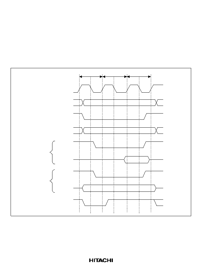
155
7.4.2
Wait State Control
The number of wait states inserted into ordinary space access states can be controlled using the
WCR and BCR1 register settings. When the Wn1 and Wn0 wait specification bits in WCR for the
given CS space are 01 or 10, software waits are inserted according to the wait specification. When
Wn1 and Wn0 are 11, wait cycles are inserted according to the long wait specification bit AnLW
in BCR1. The long wait specification in BCR1 can be made independently for CS0 and CS1
spaces, but the same value must be specified for CS2 and CS3 spaces. All WCR specifications are
independent. A Tw cycle as long as the number of specified cycles is inserted as a wait cycle at the
wait timing for ordinary access space shown in figure 7.11.
T1
Tw
CKIO
Read
Write
A26A0
CSn
RD/
WR
RD
D31D0
WEn
D31D0
BS
T2
Figure 7.11 Wait Timing of Ordinary Space Access (Software Wait Only)
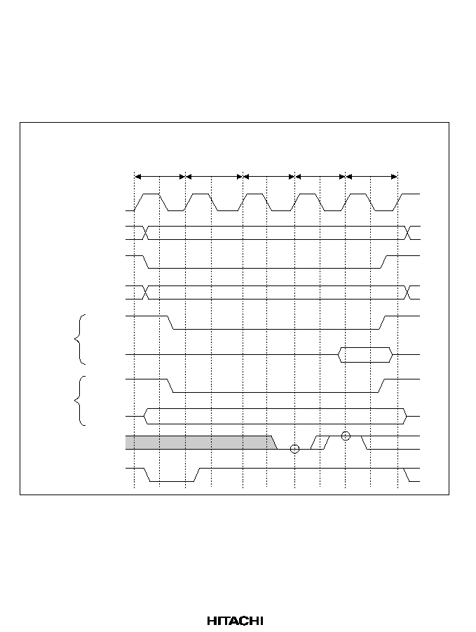
156
When the wait is specified by software using WCR, the wait input
WAIT signal from outside is
sampled. Figure 7.12 shows
WAIT signal sampling. A 2-cycle wait is specified as a software wait.
The sampling is performed when the Tw state shifts to the T2 state, so there is no effect even when
the
WAIT signal is asserted in the T1 cycle or the first Tw cycle. The WAIT signal is sampled at
the clock rise. External waits should not be inserted, however, into word accesses of devices (such
as ordinary space and burst ROM) that have an 8-bit bus width (byte-size devices). Control waits
in such cases with software only.
T1
Tw
Clock
Read
Write
A26A0
CSn
WAIT
RD/
WR
RD
D31D0
WEn
D31D0
BS
Tw
Wait states
from
WAIT
signal input
Twx
T2
Figure 7.12 Wait State Timing of Ordinary Space Access
(Wait States from
WAIT Signal)

157
7.5
Synchronous DRAM Interface
7.5.1
Synchronous DRAM Direct Connection
2-Mbit (128k
×
16), 4-Mbit (256k
×
16), and 16-Mbit (1M
×
16, 2M
×
8, and 4M
×
4)
synchronous DRAMs can be connected directly to the SH7604
.
All of these are internally divided
into two banks. Since synchronous DRAM can be selected by the
CS signal, areas CS2 and CS3
can be connected using a common
RAS or other control signal.
When the enable bits for DRAM
and other memory (DRAM2DRAM0) in BCR1 are set to 001, CS2 is ordinary space and CS3 is
synchronous DRAM space. When set to 100, CS2 is synchronous DRAM space and CS3 is
ordinary space. When set to 101, both CS2 and CS3 are synchronous DRAM spaces.
The supported synchronous DRAM operating mode is for burst read and single write. The burst
length depends on the data bus width, comprising 4 bursts for a 32-bit width, and 8 bursts for a 16-
bit width. The data bus width is specified by the SZ bit in MCR. Burst operation is always
performed, so the burst enable (BE) bit in MCR is ignored.
Control signals for directly connecting synchronous DRAM are the
RAS/CE, CAS/OE, RD/WR,
CS2 or CS3, DQMUU, DQMUL, DQMLU, DQMLL, and CKE signals
.
Signals other than
CS2
and
CS3 are common to every area, and signals other than CKE are valid and fetched only when
CS2 or CS3 is true
.
Therefore, synchronous DRAM of multiple areas can be connected in parallel.
CKE is negated (to the low level); only when a self-refresh is performed otherwise it is asserted
(to the high level).
Commands can be specified for synchronous DRAM using the
RAS/CE, CAS/OE, RD/WR, and
certain address signals. These commands are NOP, auto-refresh (REF), self-refresh (SELF), all-
bank precharge (PALL), specific bank precharge (PRE), row address strobe/bank active (ACTV),
read (READ), read with precharge (READA), write (WRIT), write with precharge (WRITA), and
mode register write (MRS).
Bytes are specified using DQMUU, DQMUL, DQMLU, and DQMLL. The read/write is
performed on the byte whose DQM is low. For 32-bit data, DQMUU specifies 4n address access
and DQMLL specifies 4n + 3 address access. For 16-bit data, only DQMLU and DQMLL are
used. Figure 7.13 shows an example in which a 32-bit connection uses a 256k
×
16 bit
synchronous DRAM. Figure 7.14 shows an example with a 16-bit connection.
158
A11
A2
CKIO
CKE
CSn
RAS
/
CE
CAS
/
OE
RD/
WR
D31
D16
CASHH
/DQMUU/
WE3
CASHL
/DQMUL/
WE2
D15
D0
CASLH
/DQMLU/
WE1
CASLL
/DQMLL/
WE0
A9
A0
CLK
CKE
CS
RAS
CAS
WE
I/O15
I/O0
DQMU
DQML
SH7604
256 k
×
16-bit
synchronous
DRAM
...
...
...
...
...
...
...
...
A9
A0
CLK
CKE
CS
RAS
CAS
WE
I/O15
I/O0
DQMU
DQML
...
...
...
...
...
...
Figure 7.13 Synchronous DRAM 32-bit Device Connection
159
A10
A1
CKIO
CKE
CSn
RAS
/
CE
CAS
/
OE
RD/
WR
D15
D0
CASLH
/DQMLU/
WE1
CASLL
/DQMLL/
WE0
A9
A0
CLK
CKE
CS
RAS
CAS
WE
I/O15
I/O0
DQMU
DQML
SH7604
256 k
×
16-bit
synchronous
DRAM
...
...
...
...
...
...
...
...
Figure 7.14 Synchronous DRAM 16-bit Device Connection
7.5.2
Address Multiplexing
Addresses are multiplexed according to the MCR's address multiplex specification bits AMX2
AMX0 and size specification bit SZ so that synchronous DRAMs can be connected directly
without an external multiplex circuit
.
Table 7.4 shows the relationship between the multiplex
specification bits and bit output to the address pins.
A26A14 and A0 always output the original value regardless of multiplexing.
When SZ = 0, the data width on the synchronous DRAM side is 16 bits and the LSB of the
device's address pins (A0) specifies word address. The A0 pin of the synchronous DRAM is thus
connected to the A1 pin of the SH7604, the rest of the connection proceeding in the same order,
beginning with the A1 pin to the A2 pin.
When SZ = 1, the data width on the synchronous DRAM side is 32 bits and the LSB of the
device's address pins (A0) specifies longword address. The A0 pin of the synchronous DRAM is
thus connected to the A2 pin of the SH7604, the rest of the connection proceeding in the same
order, beginning with the A1 pin to the A3 pin.

160
Table 7.4
SZ and AMX Bits and Address Multiplex Output
Setting
External Address Pins
SZ
AMX2
AMX1
AMX0
Output Timing
A1A8
A9
A10
A11
A12
A13
1
0
0
0
Column address
A1A8
A9
A10
A11
L/H
*1
A21
*2
Row address
A9A16
A17
A18
A19
A20
A21
*2
1
0
0
1
Column address
A1A8
A9
A10
A11
L/H
*1
A22
*2
Row address
A10A17
A18
A19
A20
A21
A22
*2
1
0
1
0
Column address
A1A8
A9
A10
A11
L/H
*1
A23
*2
Row address
A11A18
A19
A20
A21
A22
A23
*2
1
0
1
1
Column address
A1A8
A9
L/H
*1
A19
*2
A12
A13
Row address
A9A16
A17
A18
A19
*2
A20
A21
1
1
1
1
Column address
A1A8
A9
L/H
*1
A18
*2
A12
A13
Row address
A9A16
A17
A17
A18
*2
A20
A21
0
0
0
0
Column address
A1A8
A9
A10
L/H
*1
A20
*2
A13
Row address
A9A16
A17
A18
A19
A20
*2
A21
0
0
1
1
Column address
A1A8
L/H
*1
A18
*2
A11
A12
A13
Row address
A9A16
A17
A18
*2
A19
A20
A21
0
1
1
1
Column address
A1A8
L/H
*1
A17
*2
A11
A12
A13
Row address
A9A16
A16
A17
*2
A19
A20
A21
AMX2AMX0 settings of 100, 101 and 110 are reserved, so do not use them. When SZ = 0, the
settings 001 and 010 are reserved as well, so do not use them either.
Notes: 1. L/H is a bit used to specify commands. It is fixed at L or H according to the access
mode.
2. Specifies bank address.
7.5.3
Burst Reads
Figure 7.15 shows the timing chart for burst reads. In the following example, 2 synchronous
DRAMs of 256k
×
16 bits are connected, the data width is 32 bits and the burst length is 4. After a
Tr cycle that performs ACTV command output, a READA command is called in the Tc cycle and
read data is accepted at internal clock falls from Td1 to Td4. Tap is a cycle for waiting for the
completion of the auto-precharge based on the READA command within the synchronous DRAM.
During this period, no new access commands are issued to the same bank. Accesses of the other
bank of the synchronous DRAM by another CS space are possible. Depending on the TRP
specification in MCR, the SH7604 determines the number of Tap cycles and does not issue a
command to the same bank during that period.

161
Figure 7.15 shows an example of the basic cycle. Because a slower synchronous DRAM is
connected, setting WCR and MCR bits can extend the cycle. The number of cycles from the
ACTV command output cycle Tr to the READA command output cycle Tc can be specified by the
RCD bit in MCR. 0 specifies 1 cycle; 1 specifies 2 cycles. For 2 cycles, a NOP command issue
cycle Trw for the synchronous DRAM is inserted between the Tr cycle and the Tc cycle. The
number of cycles between the READA command output cycle Tc and the initial read data fetch
cycle Td1 can be specified independently for areas CS2 and CS3 between 1 cycle and 4 cycles
using the W21/W20 and W31/W30 bits in WCR. The CAS latency when using bus arbitration in
the partial-share master mode can be set differently for CS2 and CS3 spaces. The number of
cycles at this time corresponds to the number of CAS latency cycles of the synchronous DRAM.
When 2 cycles or more, a NOP command issue cycle Tw is inserted between the Tc cycle and the
Td1 cycle. The number of cycles in the precharge completion waiting cycle Tap is specified by the
TRP bit in MCR. When the CAS latency is 1, a Tap cycle of 1 or 2 cycles is generated. When the
CAS latency is 2 or more, a Tap cycle equal to the TRP specification 1 is generated. During the
Tap cycle, no commands other than NOP are issued to the same bank. Figure 7.16 shows an
example of burst read timing when RCD is 1, W31/W30 is 01, and TRP is 1.
With the synchronous DRAM cycle, when the bus cycle starts in ordinary space access, the
BS
signal asserted for 1 cycle is asserted in each of cycles Td1Td4 for the purpose of the external
address monitoring described in the section on bus arbitration. When another CS space is accessed
after an synchronous DRAM read with a wait-between-buses specification of 0, the
BS signal may
be continuously asserted. The address is updated every time data is fetched while burst reads are
being performed. The burst transfer unit is 16 bytes, so address updating affects A3A1. The
access order follows the address order in 16-byte data transfers by the DMAC, but reading starts
from the address + 4 so that the last missed data in the fill operation after a cache miss can be read.
When the data width is 16 bits, 8 burst cycles are required for a 16-byte data transfer. The data
fetch cycle goes from Td1 to Td8. From Td1 to Td8, the
BS signal is asserted in every cycle.
Synchronous DRAM CAS latency is up to 3 cycles, but the CAS latency of the bus state controller
can be specified up to 4. This is so that circuits containing latches can be installed between
synchronous DRAMs and the SH7604.
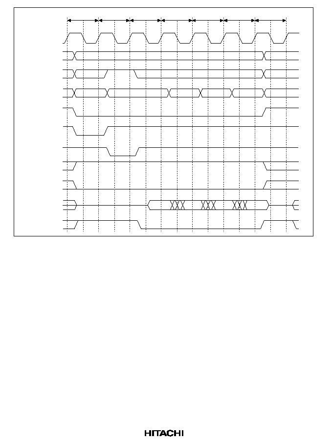
162
Tr
CKIO
A26A11
A10
A9A1
CS2
or
CS3
RAS
DQMxx
CAS
WE
D31D0
BS
Tc
Td1
Td2
Td3
Td4
Tap
Figure 7.15 Basic Burst Read Timing (Auto-Precharge)
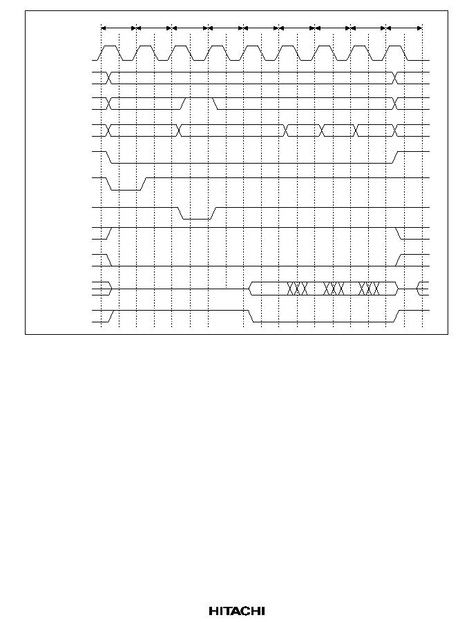
163
Tr
TrW
Tc
CKIO
A26A11
A10
A9A1
CS2
or
CS3
RAS
DQMxx
CAS
WE
D31D0
BS
Tw
Td1
Td2
Td3
Td4
Tap
Figure 7.16 Burst Read Wait Specification Timing (Auto-Precharge)

164
7.5.4
Single Reads
When a cache area is accessed and there is a cache miss, the cache fill cycle is performed in 16-
byte units. This means that all the data read in the burst read is valid. Since the required data when
a cache-through area is accessed has a maximum length of 32 bits, however, the remaining 12
bytes are wasted. The same kind of wasted data access is produced when synchronous DRAM is
specified as the source in a DMA transfer by the DMAC and the transfer unit is other than 16
bytes. Figure 7.17 shows the timing of a single address read. Because the synchronous DRAM is
set to the burst read/single write mode, the read data output continues after the required data is
received. To avoid data conflict, an empty read cycle is performed from Td2 to Td4 after the
required data is read in Td1 and the device waits for the end of synchronous DRAM operation. In
this case, data is only fetched in Td1, so the
BS signal is asserted for Td1 only.
When the data width is 16 bits, the number of burst transfers during a read is 8.
BS is asserted and
data fetched in cache-through and other DMA read cycles only in the Td1 and Td2 cycles (of the 8
cycles from Td1 to Td8) for longword accesses, and only in the Td1 cycle for word or byte
accesses.
Empty cycles tend to increase the memory access time, lower the program execution speed, and
lower the DMA transfer speed, so it is important to avoid accessing unnecessary cache-through
areas and to use data structures that enable 16-byte unit transfers by placing data on 16-byte
boundaries when performing DMA transfers that specify synchronous DRAM as the source.
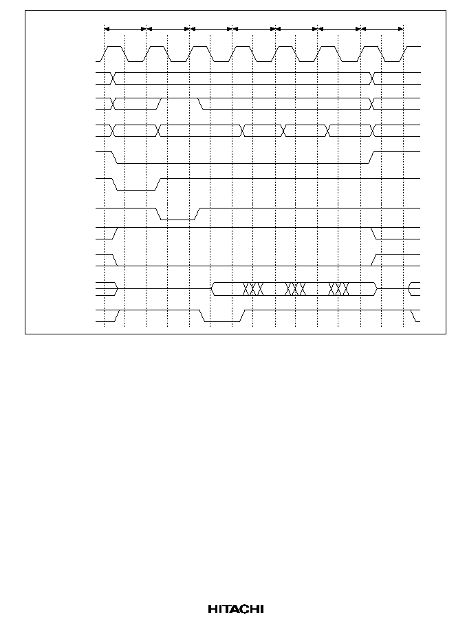
165
Tr
CKIO
A26A11
A10
A9A1
CS2
or
CS3
RAS
DQMxx
CAS
WE
D31D0
BS
Tc
Td1
Td2
Td3
Td4
Tap
Figure 7.17 Single Read Timing (Auto-Precharge)
7.5.5
Writes
Unlike synchronous DRAM reads, synchronous DRAM writes are single writes. Figure 7.18
shows the basic timing chart for write accesses. After the ACTV command Tr, a WRITA
command is issued in Tc to perform an auto-precharge. In the write cycle, the write data is output
simultaneously with the write command. When writing with an auto-precharge, the bank is
precharged after the completion of the write command within the synchronous DRAM, so no
command can be issued to that bank until the precharge is completed. For that reason, besides a
cycle Tap to wait for the precharge during read accesses, the issuing of any new commands to the
same bank during this period is delayed by adding a cycle Trw1 to wait until the precharge is
started. The number of cycles in the Trw1 cycle can be specified using the TRWL bit in MCR.
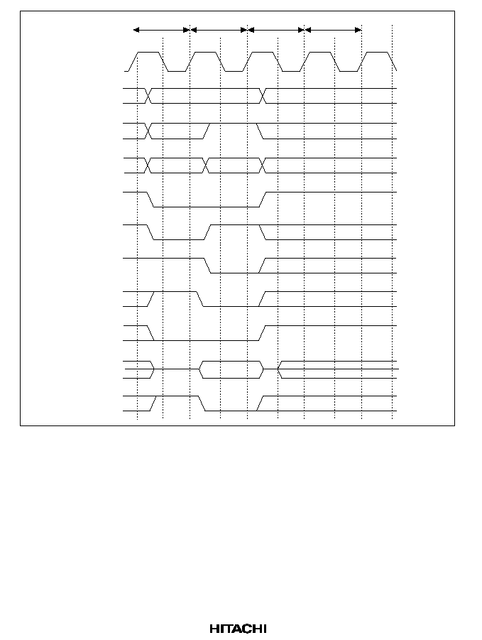
166
Tr
CKIO
A26A11
A10
A9A1
CS2
or
CS3
RAS
DQMxx
CAS
WE
D31D0
BS
Tc
Trwl
Tap
Figure 7.18 Basic Write Cycle Timing (Auto-Precharge)
7.5.6
Bank Active Function
A synchronous DRAM bank function is used to support high-speed accesses of the same row
address. When the RASD bit in MCR is set to 1, read/write accesses are performed using
commands without auto-precharge (READ, WRIT). In this case, even when the access is
completed, no precharge is performed. When accessing the same row address in the same bank, a
READ or WRIT command can be called immediately without calling an ACTV command, just
like the RAS down mode of the DRAM's high-speed page mode
.
Synchronous DRAM is divided
into two banks,
so one row address in each can stay active. When the next access is to a different
row address, a PRE command is called first to precharge the bank, and access is performed by an

167
ACTV command and READ or WRIT command, in that order, after the precharge is completed.
With successive accesses to different row addresses, the precharge is performed after the access
request occurs, so the access time is longer. When writing, performing an auto-precharge means
that no command can be called for t
RWL
+ t
AP
cycles after a WRITA command is called. When
the bank active mode is used, READ or WRIT commands can be issued consecutively if the row
address is the same. This shortens the number of cycles by t
RWL
+ t
AP
for each write. The number
of cycles between the issue of the precharge command and the row address strobe command is
determined by the TRP bit in MCR.
Whether execution is faster when the bank active mode is used or when basic access is used is
determined by the proportion of accesses to the same row address (P1) and the average number of
cycles from the end of one access to the next access (t
A
). When tA is longer than t
AP
, the delay
waiting for the precharge during a read becomes invisible. If t
A
is longer than t
RWL
+ t
AP
, the
delay waiting for the precharge also becomes invisible during writes. The difference between the
bank active mode and basic access speeds in these cases is the number of cycles between the start
of access and the issue of the read/write command: (t
RP
+ t
RCD
)
×
(1 P1) and t
RCD
,
respectively.
The time that a bank can be kept active, t
RAS
, is limited. When it is not assured that this period
will be provided by program execution and that another row address will be accessed without a hit
to the cache, the synchronous DRAM must be set to auto-refresh and the refresh cycle must be set
to the maximum value t
RAS
or less. This enables the limit on the maximum active period for each
bank to be ensured. When auto-refresh is not being used, some measure must be taken in the
program to ensure that the bank does not stay active for longer than the prescribed period.
Figure 7.19 shows a burst read cycle that is not an auto-precharge cycle, figure 7.20 shows a burst
read cycle to a same row address, figure 7.21 shows a burst read cycle to different row addresses,
figure 7.22 shows a write cycle without auto-precharge, figure 7.23 shows a write cycle to a same
row address, and figure 7.24 shows a write cycle to different row addresses.
In figure 7.20, a cycle that does nothing, Tnop, is inserted before the Tc cycle that issues the
READ command. Synchronous DRAMs, however, have a 2 cycle latency during reads for the
DQMxx signals that specify bytes. If the Tc cycle is performed immediately without inserting a
Tnop cycle, the DQMxx signal for the Td1 cycle data output cannot be specified. This is why the
Tnop cycle is inserted. When the CAS latency is 2 or more, the Tnop cycle is not inserted so that
timing requirements will be met even when a DQMxx signal is set after the Tc cycle.
When the SH7604 is set to the bank active mode, the access will start with figure 7.19 or figure
7.22 and repeat figure 7.20 or figure 7.23 for as long as the same row address continues to be
accessed when only accesses to the respective banks of the CS3 space are considered. Accesses to
other CS spaces during this period have no effect. When an access occurs to a different row
address while the bank is active, figure 7.21 or figure 7.24 will be substituted for figures 7.20 and
7.23 after this is detected. Both banks will become inactive even in the bank active mode after the
refresh cycle ends or after the bus is released by bus arbitration.
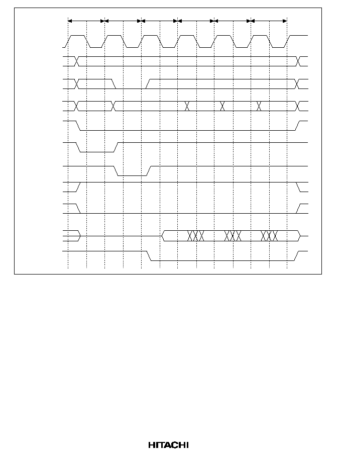
168
Tr
CKIO
A26A11
A10
A9A1
CS3
RAS
DQMxx
CAS
WE
D31D0
BS
Tc
Td1
Td2
Td3
Td4
Figure 7.19 Burst Read Timing (No Precharge)
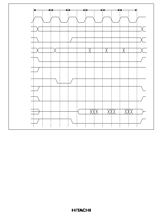
169
Tnop
CKIO
A26A11
A10
A9A1
CS3
RAS
DQMxx
CAS
WE
D31D0
BS
Tc
Td1
Td2
Td3
Td4
Figure 7.20 Burst Read Timing (Bank Active, Same Row Address)
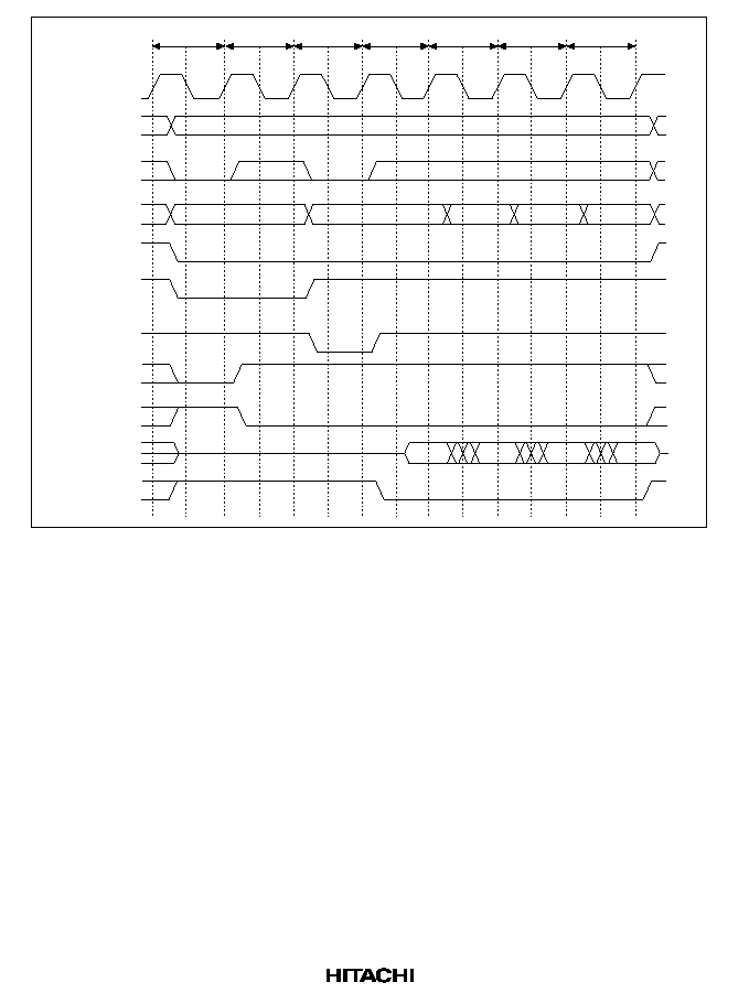
170
Tp
CKIO
A26A11
A10
A9A1
CS3
RAS
DQMxx
CAS
WE
D31D0
BS
Tr
Tc
Td1
Td2
Td3
Td4
Figure 7.21 Burst Read Timing (Bank Active, Different Row Addresses)
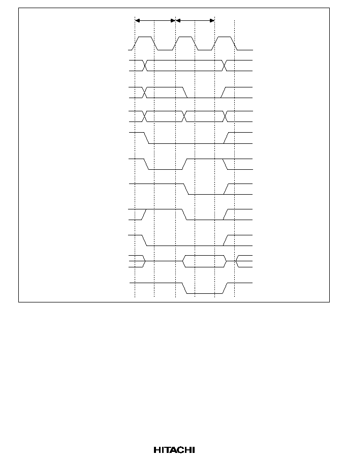
171
Tr
CKIO
A26A11
A10
A9A1
CS3
RAS
DQMxx
CAS
WE
D31D0
BS
Tc
Figure 7.22 Write Timing (No Precharge)
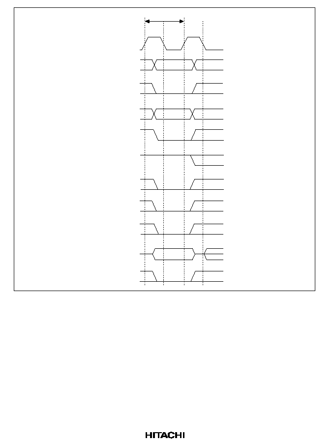
172
Tc
CKIO
A26A11
A10
A9A1
CS3
RAS
DQMxx
CAS
WE
D31D0
BS
Figure 7.23 Write Timing (Bank Active, Same Row Address)
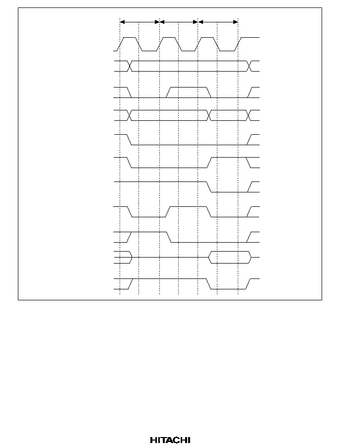
173
Tp
CKIO
A26A11
A10
A9A1
CS3
RAS
DQMxx
CAS
WE
D31D0
BS
Tr
Tc
Figure 7.24 Write Timing (Bank Active, Different Row Addresses)

174
7.5.7
Refreshes
The bus state controller is equipped with a function to control refreshes of synchronous DRAM.
Auto-refreshes can be performed by setting the MCR's RMD bit to 0 and the RFSH bit to 1. When
the synchronous DRAM is not accessed for a long period of time, set the RFSH bit and RMODE
bit both to 1 to initiate self-refresh mode, which uses low power consumption to retain data.
Auto-Refresh: Refreshes are performed at the interval determined by the input clock selected by
the CKS2CKS0 bits in RTCSR and the value set in RTCOR. Set the CKS2CKS0 bits and
RTCOR so that the refresh interval specifications of the synchronous DRAM being used are
satisfied. First, set RTCOR, RTCNT and the RMODE and RFSH bits in MCR, then set the CKS2
CKS0 bits. When a clock is selected with the CKS2CKS0 bits, RTCNT starts counting up from
the value at that time. The RTCNT value is constantly compared to the RTCOR value and a
request for a refresh is made when the two match, starting an auto-refresh. RTCNT is cleared to 0
at that time and the count up starts again. Figure 7.25 shows the timing for the auto-refresh cycle.
First, a PALL command is issued during the Tp cycle to change all the banks from active to
precharge states. A REF command is then issued in the Trr cycle. After the Trr cycle, no new
commands are output for the number of cycles specified in the TRAS bit in MCR + 2 cycles. The
TRAS bit must be set to satisfy the refresh cycle time specifications (active/active command delay
time) of the synchronous DRAM. When the MCR's TRP bit is 1, an NOP cycle is inserted
between the Tp cycle and Trr cycle.
During a manual reset, no refresh request is issued, since there is no RTCNT count-up. To perform
a refresh properly, make the manual reset period shorter than the refresh cycle interval and set
RTCNT to (RTCOR 1) so that the refresh is performed immediately after the manual reset is
cleared.
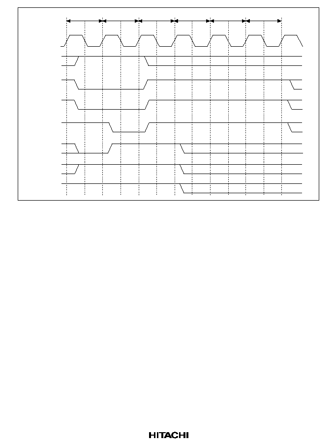
175
Tp
CKIO
A10
CS2
or
CS3
RAS
DQMxx
CAS
WE
BS
Trr
Trc
Trc
Trc
Tre
Figure 7.25 Auto-Refresh Timing
Self-Refreshes: The self-refresh mode is a type of standby mode that produces refresh timing and
refresh addresses within the synchronous DRAM. It is started up by setting the RMODE and
RFSH bits to 1. The synchronous DRAM is in self-refresh mode when the CKE signal level is
low. During the self-refresh, the synchronous DRAM cannot be accessed. To clear the self-refresh,
set the RMODE bit to 0. After self-refresh mode is cleared, issuing of commands is prohibited for
the number of cycles specified in the MCR's TRAS bit + 1 cycle. Figure 7.26 shows the self-
refresh timing. Immediately set the synchronous DRAM so that the auto-refresh is performed in
the correct interval. This ensures a correct self-refresh clear and data holding. When self-refresh
mode is entered while the synchronous DRAM is set for auto-refresh or when leaving the standby
mode with a manual reset or NMI, auto-refresh can be re-started if RFSH is 1 and RMODE is 0
when the self-refresh mode is cleared. When time is required between clearing the self-refresh
mode and starting the auto-refresh mode, this time must be reflected in the initial RTCNT setting.
When the RTCNT value is set to RTCOR 1, the refresh can be started immediately.
If the standby function of the SH7604 is used after the self-refresh is set to enter the standby
mode, the self-refresh state continues; the self-refresh state will also be maintained after returning
from a standby using an NMI.
A manual reset cannot be used to exit the self-refresh state either. During a power-on reset, the bus
state controller register is initialized, so the self-refresh state is ended.
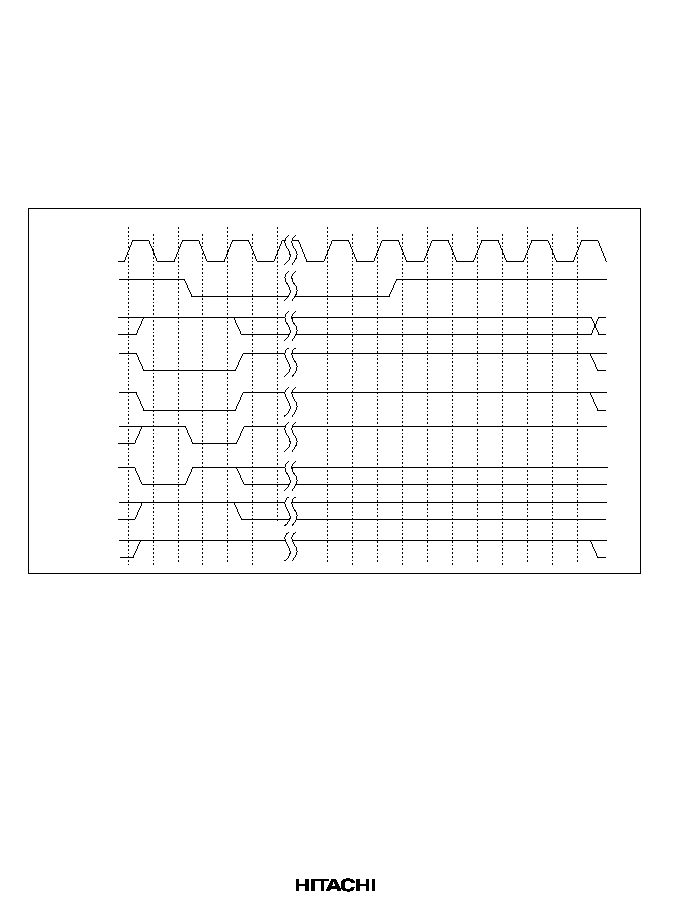
176
Refresh Requests and Bus Cycle Requests: When a refresh request occurs while a bus cycle is
executing, the refresh will not be executed until the bus cycle is completed. When a refresh request
occurs while the bus is released using the bus arbitration function, the refresh will not be executed
until the bus is recaptured. If RTCNT and RTCOR match and a new refresh request occurs while
waiting for the refresh to execute, the previous refresh request is erased. To make sure the refresh
executes properly, be sure that the bus cycle and bus capture do not exceed the refresh interval.
If a bus arbitration request occurs during a self-refresh, the bus is not released until the self-refresh
is cleared. During a self-refresh, the slave chips halt if there is a master-slave structure.
Tp
CKIO
A10
CKE
CS2
or
CS3
RAS
DQMxx
CAS
WE
BS
Trr
Trc
Trc
Trc
Trc
Trc
Tre
Figure 7.26 Self-Refresh Timing

177
7.5.8
Power-On Sequence
To use synchronous DRAM, the mode must first be set after the power is turned on. To properly
initialize the synchronous DRAM, the synchronous DRAM mode register must be written to after
the registers of the bus state controller have first been set. The synchronous DRAM mode register
is set using a combination of the
RAS/CE, CAS/OE and RD/WR signals. They fetch the value of
the address signal at that time. If the value to be set is X, the bus state controller operates by
writing to address X + H'FFFF8000 from the CPU, which allows the value X to be written to the
synchronous DRAM mode register. Data is ignored at this time, but the mode is written using
word as the size. Write any data in word size to the following addresses to select the burst read
single write supported by the SH7604, a CAS latency of 1 to 3, a sequential wrap type, and a burst
length of 8 or 4 (depending on whether the width is 16 bits or 32 bits).
For 16 bits:
CAS latency 1
CAS latency 2
CAS latency 3
H'FFFF8426
H'FFFF8446
H'FFFF8466
For 32 bits:
CAS latency 1
CAS latency 2
CAS latency 3
H'FFFF8848
H'FFFF8888
H'FFFF88C8
Figure 7.27 shows the mode register setting timing.
Writing to address X + H'FFFF8000 first issues an all-bank precharge command (PALL) in the Tp
cycle, then issues a mode register write command in the Tmw cycle. When the TRP bit in MCR is
set to 1, a single idle cycle is inserted between the Tp cycle and the Tmw cycle.
Before setting the mode register, an idle time of 100
µ
s (differs by memory manufacturer) must be
assured after the power required by the synchronous DRAM is turned on. When the pulse width of
the reset signal is longer than the idle time, the mode register may be set immediately without
problem. At least the number of dummy auto-refresh cycles specified by the manufacturer (usually
8 must be executed). After setting auto-refresh, it is usual for this to occur naturally during the
various initializations, but to make sure, the interval at which refresh requests are generated can be
shortened only while the dummy cycles are executing. Because the address counter within the
synchronous DRAM is not initialized when auto-refresh is used during single read or write
accesses, an auto-refresh cycle must always be used.
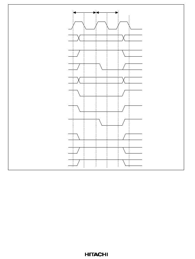
178
Tp
CKIO
A26A12
A10
A11
A9A1
CS2
or
CS3
RAS
DQMxx
CAS
WE
BS
Tmw
Figure 7.27 Synchronous DRAM Mode Write Timing

179
7.5.9
Phase Shift by PLL
The signals for synchronous DRAM interfaces change in the SH7604 at the rising edge of the
internal clock. Read data is fetched on the falling edge of an internal clock. Sampling of the
signals input by the synchronous DRAM and output of the read data, however, starts at the rising
edge of the external clock (figure 7.28).
When the internal clock of the SH7604 and external clock are synchronized, signal transmission
from the SH7604 to the synchronous DRAM has a 1 cycle margin. The transmission of read data
from the synchronous DRAM to the SH7604, however, is much tighter: only 1/2 cycle, including
the synchronous DRAM access time. When a clock system is connected without a means of
synchronization such as an on-chip PLL, transmission from the SH7604 to the synchronous
DRAM takes 1 cycle less the delay time of the clock system and transmission from the
synchronous DRAM to the SH7604 takes 1/2 cycle plus the clock system delay time. The clock
system delay time depends on the power supply voltage, temperature, and manufacturing variance,
so it has a fairly wide range. When the phase of the internal clock of the SH7604 is delayed using
a PLL that delays the phase 90 degrees relative to external clocks, transmission from the SH7604
to the synchronous DRAM and transmission from the SH7604 to the synchronous DRAM each
take 3/4 cycle.
Given this, using a clock whose phase is shifted 90 degrees from the external clock using a PLL as
the internal clock can ensure a margin of safety.
When using a PLL, it is important to note that synchronous DRAM does not contain an on-chip
PLL. When using the external clock input clock mode, instability in the clock supplied from
outside can cause shifts in phase, so a synchronization settling time in the SH7604's on-chip PLL
is needed to equalize the SH7604's internal clock and the external clock. During this
synchronization settling time, the internal clock of the synchronous DRAM and the internal clock
of the SH7604 will not always operate in perfect synchronization. To ensure the synchronous
DRAM and SH7604 operate properly, be sure that the external clock supplied is not unstable.
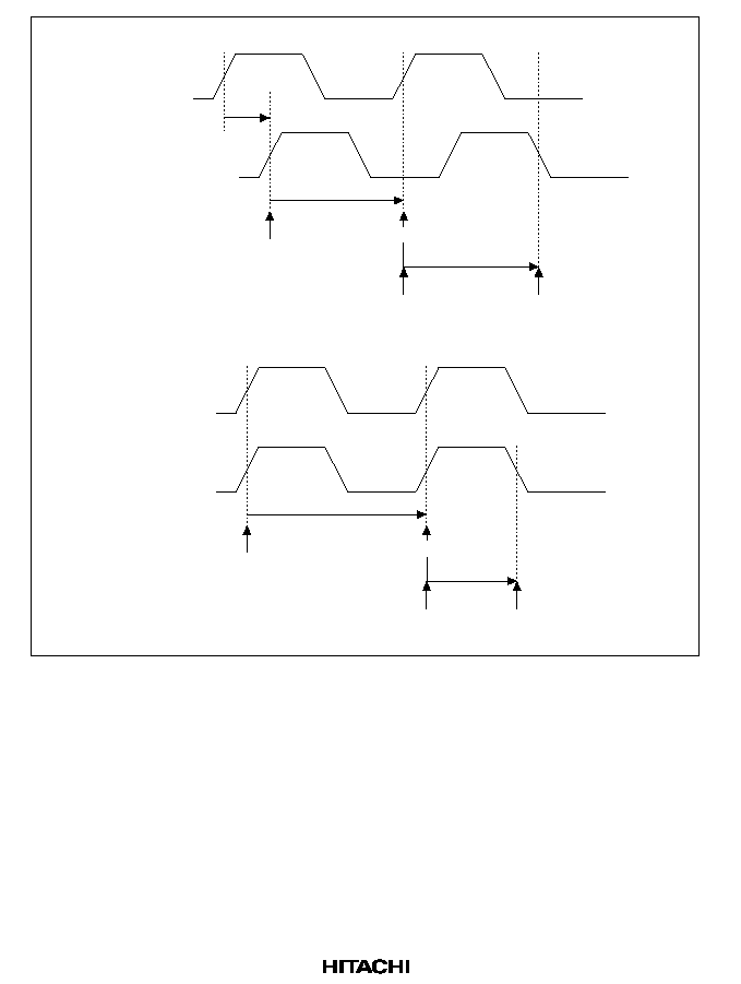
180
a. Phase Shifted 90
°
by PLL
External
CLK (CKIO)
Internal
CLK
1/4 cycle (90
°
)
3/4 cycle
3/4 cycle
Signal
output
SDRAM input latch
SDRAM
data output
Input
data latch
b. Phase Shift Using PLL is 0
External
CLK (CKIO)
Internal
CLK
1 cycle
1/2 cycle
Signal
output
SDRAM input latch
SDRAM
data output
Input
data latch
Figure 7.28 Phase Shift by PLL
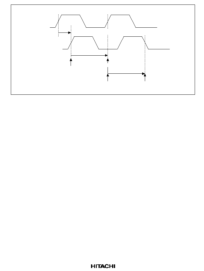
181
c. No PLL Used
External
CLK (CKIO)
Internal
CLK
1
cycle
1/2 +
cycle
Signal
output
SDRAM input latch
SDRAM
data output
Input
data latch
Clock circut delay
(fluctuates with temperature and voltage)
Figure 7.28 Phase Shift by PLL (cont)
7.6
DRAM Interface
7.6.1
DRAM Direct Connection
When the DRAM and other memory enable bits (DRAM2DRAM0) in BCR1 are set to 010, the
CS3 space becomes DRAM space, and a DRAM interface function can be used to directly connect
the SH7604 to DRAM.
The data width of an interface can be 16 or 32 bits (figures 7.29 and 7.30)
.
Two-CAS 16-bit
DRAMs can be connected, since
CAS is used to control byte access
.
The RAS,
CASHH, CASHL,
CASLH, CASLL, and RD/WR signals are used to connect the DRAM. When the data width is 16
bits,
CASHH, and CASHL are not used. In addition to ordinary read and write access, burst access
using high-speed page mode is also supported
.
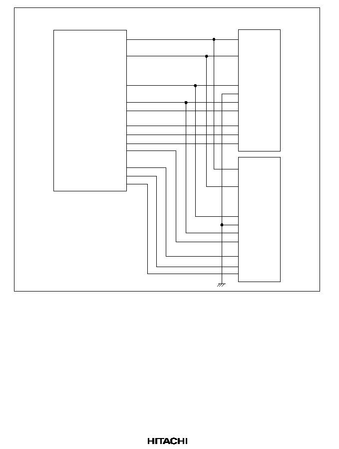
182
A10
A2
D15
D0
RAS
/
CE
RD/
WR
D31
D16
CASHH
/DQMUU/
WE3
CASHL
/DQMUL/
WE2
A8
A0
RAS
OE
WE
I/O15
I/O0
UCAS
LCAS
CASLH
/DQMLU/
WE1
CASLL
/DQMLL/
WE0
A8
A0
RAS
OE
WE
I/O15
I/O0
UCAS
LCAS
SH7604
256k
×
16 bit
DRAM
...
...
...
...
...
...
...
...
...
...
...
......
...
Figure 7.29 Example of DRAM Connection (32-Bit Data Width)
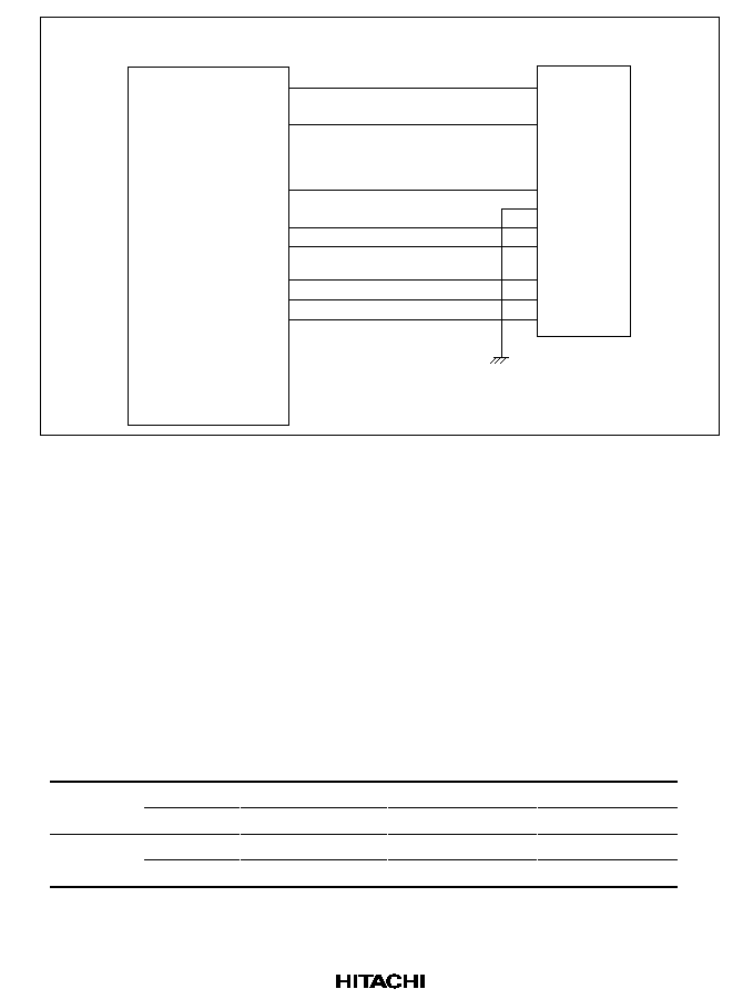
183
A9
A1
RAS
/
CE
RD/
WR
D15
D0
CASLH
/DQMLU/
WE1
CASLL
/DQMLL/
WE0
A8
A0
RAS
OE
WE
I/O15
I/O0
UCAS
LCAS
SH7604
256k
×
16 bit
DRAM
...
...
...
...
...
...
...
...
Figure 7.30 Example of DRAM Connection (16-Bit Data Width)
7.6.2
Address Multiplexing
When the CS3 space is set to DRAM, addresses are always multiplexed. This allows DRAMs that
require multiplexing of row and column addresses to be connected directly to SH7604
microprocessors without additional multiplexing circuits. There are four ways of multiplexing,
which can be selected using the MCR's AMX1AMX0 bits. Table 7.5 illustrates the relationship
between the AMX1AMX0 bits and address multiplexing. Address multiplexing is performed on
address output pins A13A1. The original addresses are output to pins A26A14. During DRAM
accesses, AMX2 is reserved, so set it to 0.
Table 7.5
Relationship between AMX1AMX0 and Address Multiplexing
AMX1
AMX0
No. of Column
Address Bits
Row
Address Output
Column
Address Output
0
0
8 bits
A21A9
A13A1
1
9 bits
A22A10
A13A1
1
0
10 bits
A23A11
A13A1
1
11 bits
A24A12
A13A1
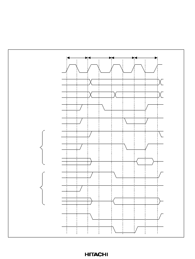
184
7.6.3
Basic Timing
The basic timing of a DRAM access is 3 cycles. Figure 7.31 shows the basic DRAM access
timing. Tp is the precharge cycle, Tr is the RAS assert cycle, Tc1 is the CAS assert cycle, and Tc2
is the read data fetch cycle. When accesses are consecutive, the Tp cycle of the next access
overlaps the Tc2 cycle of the previous access, so accesses can be performed in a minimum of 3
cycles each.
Tp
Tr
Tc1
Tc2
CKIO
Read
Write
A26A14
A13A1
RAS
CASn
RD/
WR
RD
D31D0
RD/
WR
RD
D31D0
CS3
BS
Figure 7.31 Basic Access Timing
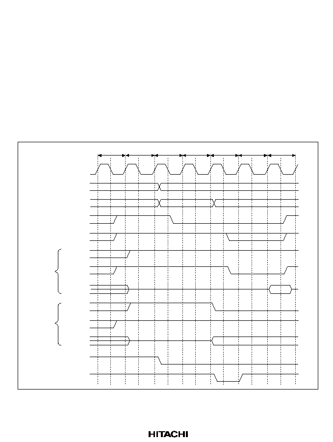
185
7.6.4
Wait State Control
When the clock frequency is raised, 1 cycle may not always be sufficient for all states to end, as in
basic access. Setting bits in WCR and MCR enables the state to be lengthened. Figure 7.32 shows
an example of lengthening a state using settings. The Tp cycle (which ensures a sufficient RAS
precharge time) can be extended to 2 cycles by insertion of a Tpw cycle by means of the TRP bit
in MCR. The number of cycles between RAS assert and CAS assert can be extended to 2 cycles
by inserting a Trw cycle by means of the RCD bit in MCR. The number of cycles from CAS assert
to the end of access can be extended from 1 cycle to 3 cycles by setting the W31/W30 bits in
WCR. When a value other than 00 is set in W31 and W30, the external wait pin
WAIT is also
sampled, so the number of cycles is further increased. Figure 7.33 shows the timing of wait state
control using the
WAIT pin. In either case, when consecutive accesses occur, the Tp cycle of one
access overlaps the Tc2 cycle of the previous access.
Tp
Tpw
Tr
Trw
Tc1
Tw
Tc2
CKIO
Read
Write
A26A14
A13A1
RAS
CASn
RD/
WR
RD
D31D0
RD/
WR
RD
D31D0
CS3
BS
Figure 7.32 Wait State Timing
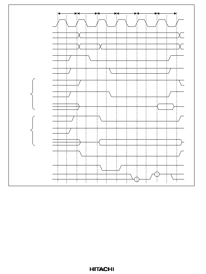
186
Tp
Tr
Tc1
Tw
Twx
Tc2
CKIO
Read
Write
A26A14
A13A1
RAS
CASn
RD/
WR
RD
D31D0
RD/
WR
RD
D31D0
CS3
BS
WAIT
Figure 7.33 External Wait State Timing
7.6.5
Burst Access
In addition to the ordinary mode of DRAM access, in which row addresses are output at every
access and data is then accessed, DRAM also has a high-speed page mode for use when
continuously accessing the same row that enables fast access of data by changing only the column
address after the row address is output. Select ordinary access or high-speed page mode by setting
the burst enable bit (BE) in MCR. Figure 7.34 shows the timing of burst operation in high-speed
page mode. When performing burst access, cycles can be inserted using the wait state control
function.
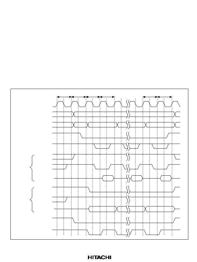
187
The SH7604 has an address comparator to detect matches of row addresses in burst mode. When
this function is used and the BE bit in MCR is set to 1, setting the MCR's RASD bit (which
specifies RAS down mode) to 1 places the SH7604 in RAS down mode, which leaves the RAS
signal asserted. Since the
CASHH, CASHL, CASLH and CASLL signals are shared with WE3,
WE2, WE1 and WE0 of ordinary space, however, write cycles to ordinary space during RAS
down mode will simultaneously initiate an erroneous write access to the DRAM. This means that
when no external devices that write to other than DRAM are connected, a DRAM can be directly
interfaced using RAS down mode. When RAS down mode is used, the refresh cycle must be less
than the maximum DRAM RAS assert time t
RAS
when the refresh cycle is longer than the t
RAS
maximum.
When an external circuit is added to keep the
CASHH, CASHL, CASLH, and CASLL signals
connected to the DRAM asserted only when the
CS3 level is low, there are no restrictions on the
use of RAS down mode.
Tp
Tr
Tc2
Tc1
Tc2
Tc1
CKIO
Read
Write
A26A14
A13A0
RAS
CASn
RD/
WR
RD
D31D0
RD/
WR
RD
D31D0
CS3
BS
Figure 7.34 Burst Access Timing
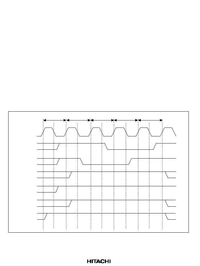
188
7.6.6
Refresh Timing
The BSC has a function for controlling DRAM refreshes. By setting the MCR's RMODE bit to 0
and RFSH bit to 1, distributed refreshing using the CAS-before-RAS refresh cycle can be
performed.
Refreshes are performed at the interval determined by the input clock selected with CKS2CKS0
in RTCSR and the value set in RTCOR. Set the values of RTCOR and CKS2CKS0 so they
satisfy the refresh interval specifications of the DRAM being used. First, set RTCOR, RTCNT and
the RMODE and RFSH bits in MCR, then set the CKS2CKS0 bits. When a clock is selected with
the CKS2CKS0 bits, RTCNT starts counting up from the value at that time. The RTCNT value is
constantly compared to the RTCOR value and a request for a refresh is made when the two match,
starting a CAS-before-RAS refresh. RTCNT is cleared to 0 at that time and the count up starts
again. Figure 7.35 shows the timing for the CAS-before-RAS refresh cycle.
The number of RAS assert cycles in the refresh cycle is specified by the TRAS bit in MCR. As
with ordinary accesses, the specification of the RAS precharge time in refresh cycles follows the
setting of the TRP bit in MCR.
Tp
Trr
Trc1
Trc2
Tre
CKIO
RAS
CASn
RD/
WR
RD
CS3
BS
Figure 7.35 Refresh Cycle Timing

189
7.6.7
Power-On Sequence
When DRAM is used after the power is turned on, there is a requirement for a waiting period
during which accesses cannot be performed (100
µ
s or 200
µ
s minimum) followed by the
prescribed number of dummy CAS-before-RAS refresh cycles (usually 8). The bus state controller
does not perform any special operations for the power-on reset, so the required power-on sequence
must be implemented by the initialization program executed after a power-on reset.
7.7
Pseudo-SRAM Interface
7.7.1
Pseudo-SRAM Direct Connection
When the DRAM and other memory enable bits (DRAM2DRAM0) in BCR1 are set to 011, the
CS3 space becomes pseudo-SRAM space, and the pseudo-SRAM interface function can be used to
directly connect the SH7604 to pseudo-SRAM. The interface data width is 16 or 32 bits.
The refresh and output enable signals of the connected pseudo-SRAM are multiplexed. The
signals used for connecting pseudo-SRAM are the
CE, OE, WE3, WE2, WE1, and WE0 signals
.
The
WE3 and WE2 signals are not used when the data width is 16 bits. When non-multiplexed
pseudo-SRAM is connected, the
RD signal is also used.
In addition to ordinary read and write access, burst access using the static column access function
is also supported
.
Figure 7.36 shows an example of connections to 1-M pseudo-SRAM with
separate
OE and RFSH pins; figure 7.37 shows an example of connections to 4-M pseudo-SRAM
with multiplexed
OE/RFSH pins. 256-k pseudo-SRAM is multiplexed in the same way as 4-M
pseudo-SRAM. All data widths are 32 bits.
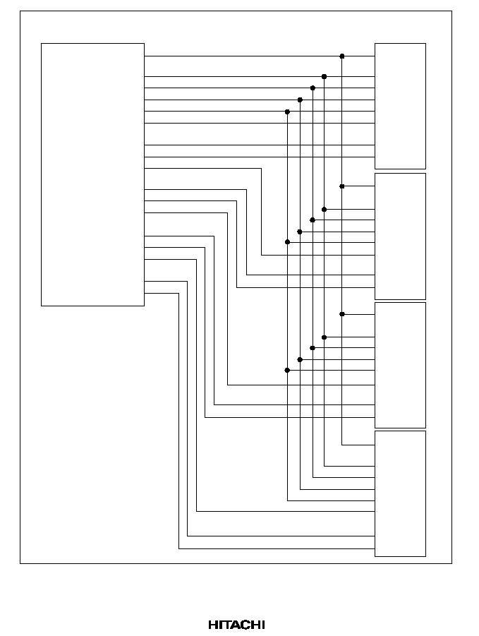
190
...
...
A16
A0
CE
OE
RFSH
I/O7
I/O0
WE
...
...
A16
A0
CS
OE
RFSH
I/O7
I/O0
WE
...
...
A16
A0
CS
OE
RFSH
I/O7
I/O0
WE
...
...
...
...
...
...
...
...
...
......
...
...
...
...
A16
A0
CS
OE
RFSH
I/O7
I/O0
WE
...
...
...
......
A18
A2
RAS
/
CE
RD
CAS
/
OE
CASHH
/DQMUU/
WE3
CASHL
/DQMUL/
WE2
CASLH
/DQMLU/
WE1
CASLL
/DQMLL/
WE0
D31
D24
D23
D16
D15
D8
D7
D0
128k
×
8 bit
pseudo-SRAM
SH7604
Figure 7.36 Example of Pseudo-SRAM Connection (1-Mbit Pseudo-SRAM)
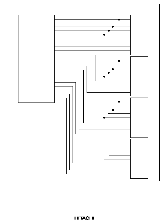
191
...
...
A18
A0
CE
OE
/
RFSH
I/O7
I/O0
WE
...
...
A18
A0
CS
OE
/
RFSH
I/O7
I/O0
WE
...
...
A18
A0
CS
OE
/
RFSH
I/O7
I/O0
WE
...
...
...
...
...
...
...
...
...
......
...
...
...
...
A18
A0
CS
OE
/
RFSH
I/O7
I/O0
WE
...
...
...
......
A20
A2
RAS
/
CE
CAS
/
OE
CASHH
/DQMUU/
WE3
CASHL
/DQMUL/
WE2
CASLH
/DQMLU/
WE1
CASLL
/DQMLL/
WE0
D31
D24
D23
D16
D15
D8
D7
D0
512k
×
8 bit
pseudo-SRAM
SH7604
Figure 7.37 Example of Pseudo-SRAM Connection (4-Mbit Pseudo-SRAM)
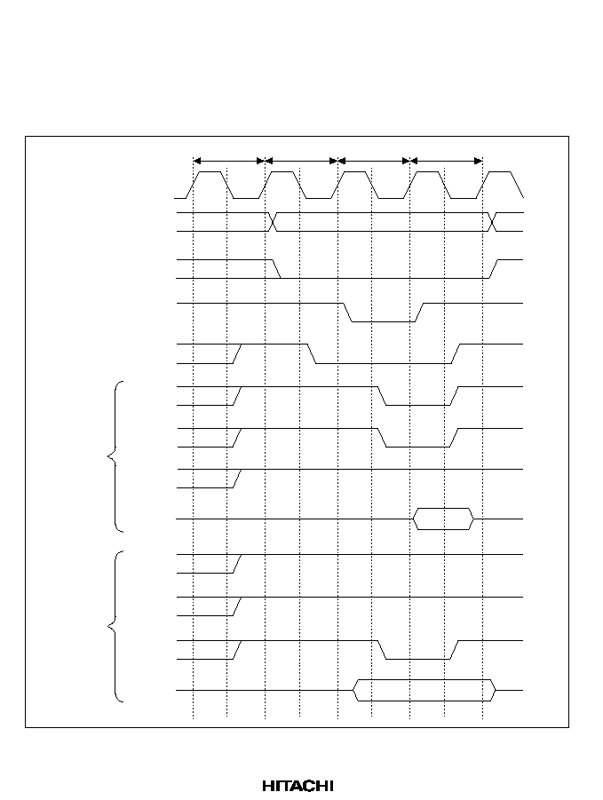
192
7.7.2
Basic Timing
Figure 7.38 shows the basic pseudo-SRAM access timing. Tp is the precharge cycle, Tr is the
CE
assert cycle, Tc1 is the write data output and
BS assert cycle, and Tc2 is the read data fetch cycle.
When accesses are consecutive, precharge cycle Tp overlaps the Tc2 cycle of the previous access,
so reads or writes can be performed in a minimum of 3 cycles each.
Tp
Tr
Tc1
Tc2
CKIO
Read
Write
A26A1
CS3
BS
CE
OE
RD
WEn
D31D0
OE
RD
WEn
D31D0
Figure 7.38 Basic Access Timing
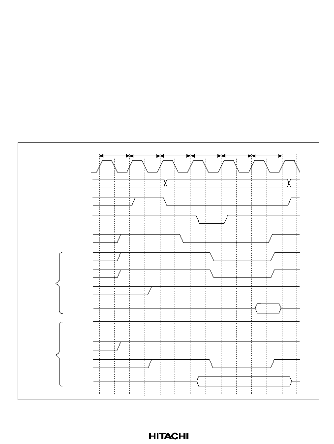
193
7.7.3
Wait State Control
When the clock frequency is raised, 1 cycle may not always be sufficient for all states to end, as in
basic access. Setting bits in WCR and MCR enables the state to be lengthened. Figure 7.39 shows
an example of lengthening a state using settings. The Tp cycle that ensures a sufficient
CE
precharge time can be extended to 2 cycles by insertion of a Tpw cycle by means of the TRP bit in
MCR. The number of cycles between
BS assert and the end of access can be extended from 2 to 4
cycles by setting the W31/W30 bits in WCR. When a value other than 00 is set in W31 and W30,
the external wait pin
WAIT is also sampled, so the number of cycles can be further increased.
Figure 7.40 shows the timing of wait state control using the
WAIT pin. In either case, when
consecutive accesses occur, the Tp cycle of one access overlaps the Tc2 cycle of the previous
access. The RCD bit in MCR is set to 0 for a pseudo-SRAM interface, but when set to 1, the
number of cycles from the
CE assert to the BS assert or write data output becomes 2.
Tp
Tr
Tc1
Tw
Tc2
Tpw
CKIO
Read
Write
A26A1
CS3
BS
CE
OE
RD
WEn
D31D0
OE
RD
WEn
D31D0
Figure 7.39 Wait State Timing
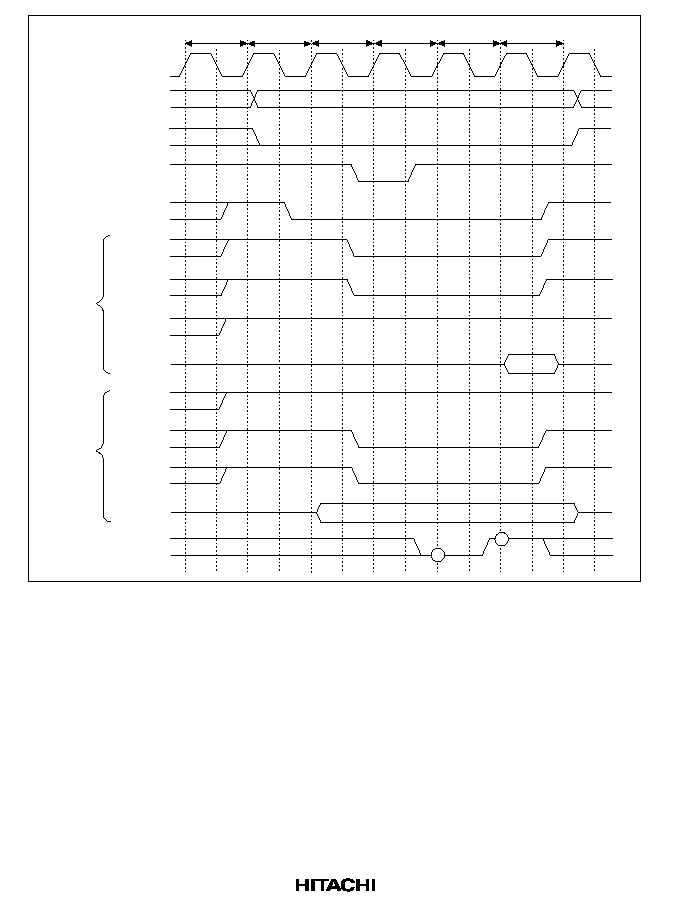
194
Tp
Tc1
Tw
TwX
Tc2
Tr
CKIO
Read
Write
A26A1
CS3
BS
CE
OE
RD
WEn
D31D0
OE
RD
WEn
WAIT
D31D0
Figure 7.40 External Wait State Timing
7.7.4
Burst Access
In addition to normal access, in which CE is alternatively asserted and negated at every access,
when consecutive accesses are to the same row address the pseudo-SRAM can access data at high
speed by changing only the column address and leaving CE asserted. This function is called the
static column mode. Select between ordinary access and burst mode using static column mode by
setting the burst enable bit (BE) in MCR. Figure 7.41 shows the timing of burst operation using
static column mode. When performing burst access, cycles can be inserted using the wait state
control function.
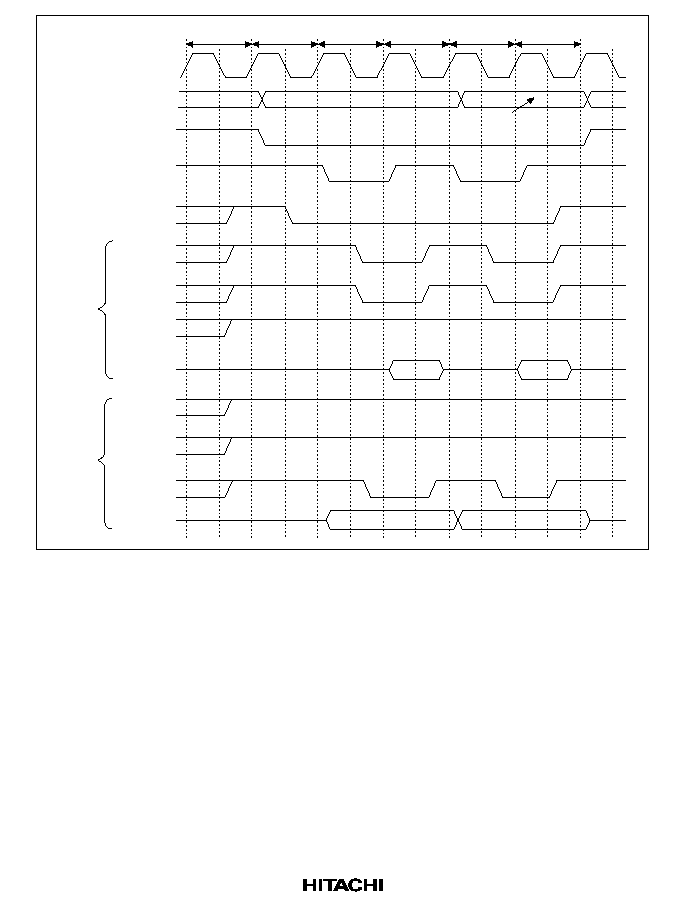
195
Tp
Tr
Tc1
Tc2
Tc1
Tc2
CKIO
Read
Write
A26A1
CS3
BS
CE
OE
RD
WEn
D31D0
OE
RD
WEn
D31D0
Only column
address changes
Figure 7.41 Static Column Mode
7.7.5
Refreshing
The BSC has a function for controlling pseudo-SRAM refreshing. By setting the MCR's RMODE
bit to 0 and RFSH bit to 1, distributed refreshing using the auto-refresh cycle can be performed.
Refreshes are performed at the interval determined by the input clock selected with CKS2CKS0
in RTCSR and the value set in RTCOR. Set the values of RTCOR and CKS2CKS0 so they
satisfy the refresh interval specifications of the pseudo-SRAM being used. First, set RTCOR,
RTCNT and the RMODE and RFSH bits in MCR, then set the CKS2CKS0 bits. When a clock is
selected with the CKS2CKS0 bits, RTCNT starts counting up from the value at that time. The
RTCNT value is constantly compared to the RTCOR value and a request for a refresh is made
when the two match, starting an auto-refresh. RTCNT is cleared to 0 at that time and the count up
starts again. Figure 7.42 shows the timing for the auto-refresh cycle.
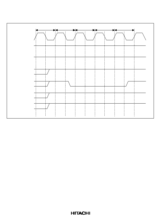
196
The number of
OE assert cycles for auto-refresh is specified by the TRAS bit in MCR. As with
ordinary accesses, the specification of the precharge time from
OE negation to the next CE assert
follows the setting of the TRP bit in MCR.
Tp
Trr
Trc
Trc
Tre
CKIO
CS3
CE
BS
OE
/
RFSH
RD
WEn
Figure 7.42 Auto-Refresh
The self-refresh mode is initiated in the pseudo-SRAM when the
RFSH signal stays low for a
prescribed period of time. A self-refresh is started by setting the RMODE and RFSH bits to 1.
During the self-refresh, the pseudo-SRAM cannot be accessed. To clear self-refreshing, set either
the RMODE or RFSH bit to 0. After self-refresh mode is cleared, issuing of commands is
inhibited for 1 auto-refresh cycle. If more time than this is required to return from self-refresh,
write the program so that there are no accesses to the pseudo-SRAM, including auto-refreshes,
during this period. Figure 7.43 shows the self-refresh timing. After self-refreshing is cleared,
immediately set the pseudo-SRAM so that auto-refresh is performed in the correct interval. This
ensures correct self-refresh clearing and data retention. When time is required between clearing
the self-refreshing and initiating the auto-refresh mode, this time must be reflected in the initial
RTCNT setting.
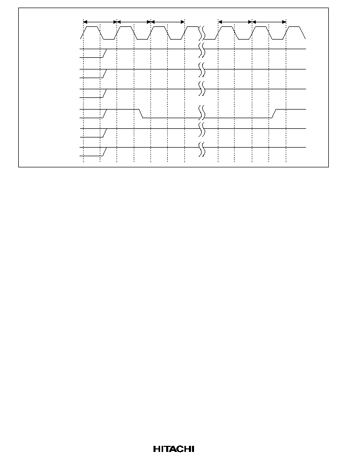
197
Tp
Trr
Trc
Trc
Tre
CKIO
CS3
CE
BS
OE
/
RFSH
RD
WEn
Figure 7.43 Self-Refresh
7.7.6
Power-On Sequence
When pseudo-SRAM is used after the power is turned on, there is a requirement for a waiting
period during which accesses cannot be performed (100
µ
s minimum) followed by the prescribed
number of dummy auto-refresh cycles (usually 8). The bus state controller does not perform any
special operations for the power-on reset, so the required power-on sequence must be implemented
by the initialization program executed after a power-on reset.
7.8
Burst ROM Interface
Set the BSTROM bit in BCR1 to set the CS0 space for connection to burst ROM. The burst ROM
interface is used to permit fast access to ROMs that have the nibble access function. Figure 7.44
shows the timing of nibble accesses to burst ROM. Set for two wait cycles. The access is basically
the same as an ordinary access, but when the first cycle ends, only the address is changed. The
CS0 signal is not negated, enabling the next access to be conducted without the T1 cycle required
for ordinary space access. From the second time on, the T1 cycle is omitted, so access is 1 cycle
faster than ordinary accesses. Currently, the nibble access can only be used on 4-address ROM.
This function can only be utilized for word or longword reads to 8-bit ROM and longword reads to
16-bit ROM. Mask ROMs have slow access speeds and require 4 instruction fetches for 8-bit
widths and 16 accesses for cache fills. Limited support of nibble access was thus added to alleviate
this problem. When connecting to an 8-bit width ROM, a maximum of 4 consecutive accesses are
performed; when connecting to a 16-bit width ROM, a maximum of 2 consecutive accesses are
performed. Figure 7.45 shows the relationship between data width and access size. For cache fills
and DMAC 16-byte transfers, longword accesses are repeated 4 times.
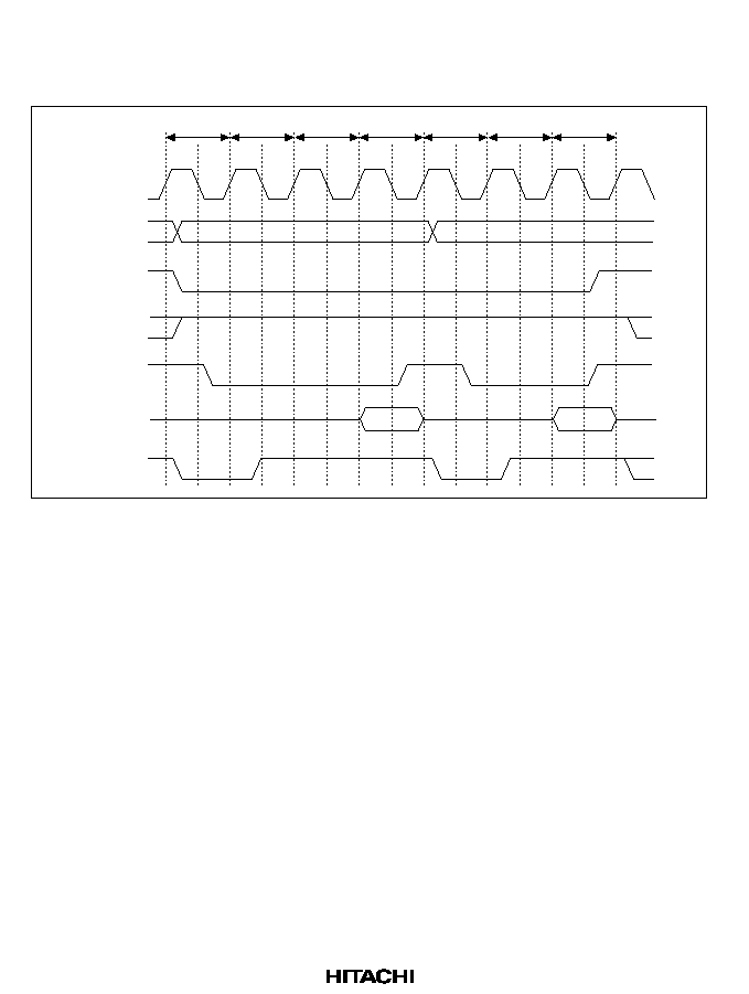
198
When one or more wait states are set for a burst ROM access, the
WAIT pin is sampled. When the
burst ROM is set and 0 specified for waits, there are 2 access cycles from the second time on.
Figure 7.46 shows the timing.
T1
Tw1
Tw2
T2
Tw1
Tw2
T2
CKIO
A26A0
RD/
WR
CS0
RD
D31D0
BS
Figure 7.44 Burst ROM Nibble Access (2 Wait States)
199
T1
Tw
T2
Tw
T2
Tw
T2
Tw
T2
8-bit bus-width longword access
T1
Tw
T2
Tw
T2
8-bit bus-width access
T1
Tw
T2
8-bit bus-width byte access
T1
Tw
T2
Tw
T2
16-bit bus-width longword access
T1
Tw
T2
16-bit bus-width word access
T1
Tw
T2
16-bit bus-width byte access
T1
Tw
T2
32-bit bus-width longword access
T1
Tw
T2
32-bit bus-width word access
T1
Tw
T2
32-bit bus-width byte access
Figure 7.45 Data Width and Burst ROM Access (1 Wait State)
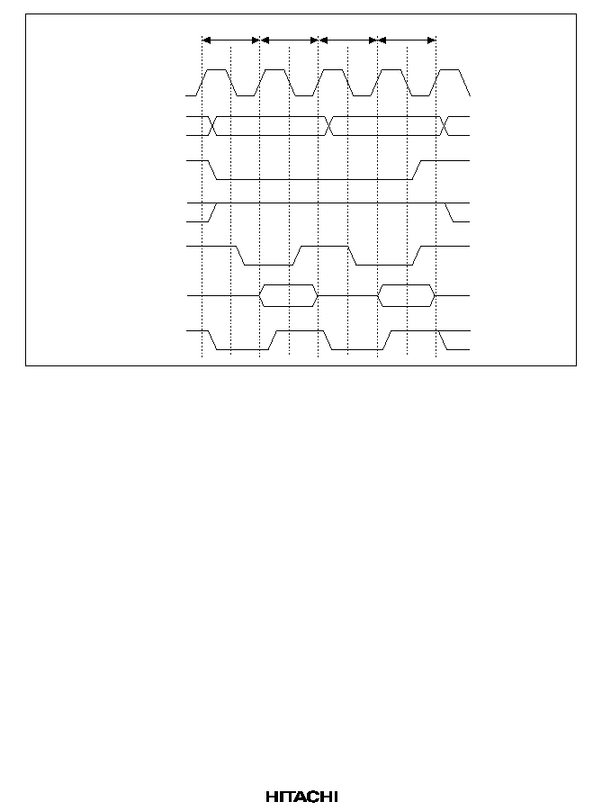
200
T1
T2
T1
T2
CKIO
A26A0
RD/
WR
CS0
RD
D31D0
BS
Figure 7.46 Burst ROM Nibble Access (No Wait States)
7.9
Waits between Access Cycles
Because operating frequencies have become high, when a read from a slow device is completed,
data buffers may not go off in time to prevent data conflicts with the next access. This lowers
device reliability and causes errors. To prevent this, a function has been added to avoid data
conflicts that memorizes the space and read/write state of the preceding access and inserts a wait
in the access cycle for those cases in which problems are found to occur when the next access
starts up. Checks are performed in two cases: if a read cycle is followed immediately by a read
access to a different CS space, and if a read access is followed immediately by a write from the
SH7604. When the SH7604 is writing continuously, if the format is always to have the direction
of the data from the SH7604 to other memory, there are no particular problems. Neither is there
any particular problem if the following read access is to the same CS space, since data is output
from the same data buffer. The number of idle cycles to be inserted into the access cycle when
reading from another CS space, or performing a write, after a read from the CS3 space, is specified
by the IW31 and IW30 bits in WCR. Likewise, IW21 and IW20 specify the number of idle cycles
after CS2 reads, IW11 and IW10 specify the number after CS1 reads, and IW01 and IW00 specify
the number after CS0 reads. From 0 to 2 cycles can be specified. When there is already a gap
between accesses, the number of empty cycles is subtracted from the number of idle cycles before
insertion. When a write cycle is performed immediately after a read access, 1 wait cycle is inserted
even when 0 is specified for waits between access cycles.
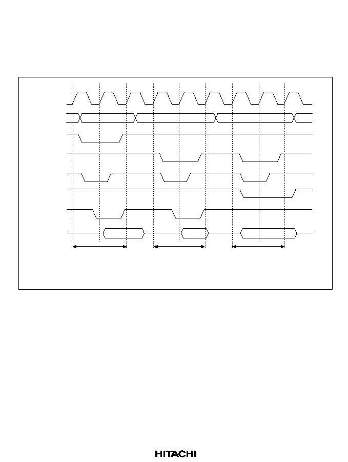
201
When the SH7604 shifts to a read cycle immediately after a write, the write data becomes high
impedance when the clock rises, but the
RD signal, which indicates read cycle data output enable,
is not asserted until the clock falls. The result is that no waits are inserted into the access cycle.
When bus arbitration is being performed, an empty cycle is inserted for arbitration, so no wait is
inserted between cycles.
T1
T2
Twait
T1
T2
Twait
T1
T2
CKIO
A26A0
RD/WR
CSm
CSn
RD
D31D0
BS
CSm space read
Specification of waits
between CSm accesses
(reading different spaces)
Specification of waits
between CSn accesses
(read followed by write)
CSn space read
CSn space write
Figure 7.47 Waits between Access Cycles
7.10
Bus Arbitration
The SH7604 has a bus arbitration function that, when a bus release request is received from an
external device, releases the bus to that device after the bus cycle being executed is completed. In
addition, it also has a bus arbitration function for supporting the connection of two processors.
These are connected to each other as master and slave through bus arbitration, which enables a
multiprocessor system to be implemented with a minimum of hardware.
There are three modes for bus arbitration: master mode, partial-share master mode, and slave
mode. Master mode keeps the bus under normal conditions and permits other devices to use the
bus by releasing it when they request its use. The slave mode normally does not have the bus. The
bus is requested when an external bus access cycle comes up and then releases the bus when the

202
access is completed. The partial-share master mode only shares CS2 space with external devices.
For the CS2 space, the mode is slave mode; for other spaces, the bus is held constantly without
any bus arbitration. Which CS space of the chip in master mode the CS2 space of the chip in
partial-share master mode is allocated to, is determined by external circuitry.
Master or slave mode can be specified using external mode pins. Partial-share master mode is
reached from master mode by a software setting. See Section 3, Oscillator Circuits and Operating
Modes, for the external mode pin settings. When a device in master or slave mode does not have
the bus, the bus goes to high impedance, so the master mode chip and slave mode chips can be
connected directly. In the partial-share master mode, the bus is always driven, so an external
buffer is needed to connect to a master bus. In master mode, a connection to an external device
requesting the bus can be substituted for the slave mode connection. In the following explanation,
external devices requesting the bus are also called slaves.
The SH7604 has two internal bus masters, the CPU and the DMAC. When synchronous DRAM,
DRAM or pseudo-SRAM is connected and refresh control is performed, the refresh request
becomes a third master. In addition to these, there are also bus requests from external devices
while in the master mode. The priority for bus requests when they occur simultaneously is, highest
to lowest, refresh requests, bus requests from external devices, DMAC and CPU.
When the bus is being passed between slave and master, all bus control signals are negated before
the bus is released to prevent erroneous operation of the connected devices. Once the bus is
received, the bus control signals change from negated to bus driven. The master and slave passing
the bus between them drive the same signal values, so output buffer conflict is avoided. Turning
the output buffer off for the bus control signals on the side that releases the bus and on at the side
acquiring the bus can eliminate the high impedance period of the signals. It is usually not
necessary to insert a pull-up resistance into these control signals to prevent malfunction caused by
external noise while they are at high impedance.
Bus permission is granted at the end of the bus cycle. When the bus is requested, the bus is
released immediately if there is no ongoing bus cycle. If there is a current bus cycle, the bus is not
released until the bus cycle ends. Even when there does not appear to be an ongoing bus cycle
when seen from outside the SH7604, it cannot be determined whether or not the bus will be
released immediately when a bus control signal such as a
CSn signal is seen, since an internal bus
cycle, such as inserting a wait between access cycles, may have been started. The bus cannot be
released during burst transfers for cache fills or 16-byte DMAC block transfers. Likewise, the bus
cannot be released between the read and write cycles of a TAS instruction. Arbitration is also not
performed between multiple bus cycles produced by a data width smaller than the access size,
such as a longword access to an 8-bit data width memory. Bus arbitration is performed between
external vector fetch, PC save, and SR save cycles during interrupt handling, which are all
independent accesses.
Because the CPU in the SH7604 is connected to cache memory by a dedicated internal bus, cache
memory can be read even when the bus is being used by another bus master on the chip or

203
externally. Writing from the CPU always produces a write cycle externally since the write-through
system is used by the SH7604 for the cache. When an external bus address monitor is not specified
by the user break controller, the internal bus that connects the CPU, DMAC and on-chip
peripheral modules can operate in parallel to the external bus. This means that both read and write
accesses from CPU to on-chip peripheral modules and from DMAC to on-chip peripheral module
are possible. If an external bus address monitor is specified, the internal bus will be used for
address monitoring when the bus is passed to the external bus master, so accesses to on-chip
peripheral modules by the CPU and DMAC must wait for the bus to be returned.
7.10.1
Master Mode
Master mode processors keep the bus unless they receive a bus request. When a bus release
request (
BRLS) assertion (low level) is received from an external device, buses are released and a
bus grant (
BGR) is asserted (low level) as soon as the bus cycle being executed is completed.
When it receives a negated (high level)
BRLS signal, indicating that the slave has released the bus,
it negates the
BGR (to high level) and begins using the bus. When the bus is released, all output
and I/O signals related to the bus interface are changed to high impedance, except for the CKE
signal for the synchronous DRAM interface, the
BGR signal for bus arbitration, and DMA transfer
control signals DACK0 and DACK1.
When the DRAM or pseudo-SRAM has finished precharging, the bus is released. The
synchronous DRAM also issues a precharge command to the active bank or banks. After this is
completed, the bus is released.
The specific bus release sequence is as follows. First, the bus use enable signal is asserted
synchronously with the fall of the clock. Half a cycle later, the address bus and data bus become
high impedance synchronous with the rise of the clock. Thereafter the bus control signals (
BS,
CSn, RAS, CAS, WEn, RD, RD/WR, IVECF) become high impedance with the fall of the clock.
All of these signals are negated at least 1.5 cycles before they become high impedance. Sampling
for bus request signals occurs at the clock fall.
The sequence when the bus is taken back from the slave is as follows. When the negation of
BRLS
is detected at a clock fall,
BGR is immediately negated and the master simultaneously starts to
drive the bus control signals. The address bus and data bus are driven starting at the next clock
rise. The bus control signals are asserted and the bus cycle actually starts from the same clock rise
at which the address and data signals are driven, at the earliest. Figure 7.48 shows the timing of
bus arbitration in master mode.
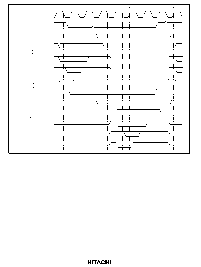
204
Address
data
BS
RD
WEn
CSn
RD/
WR
BACK
BREQ
Address
data
CKIO
BS
RD
WEn
CSn
RD/
WR
BGR
BRLS
Master
mode
side
Slave
mode
side
Figure 7.48 Bus Arbitration
When a refresh request is generated in the SH7604 while
BGR is asserted and the bus released, the
BGR may or may not be negated.
Case in Which
BGR is Negated: If access processing for an external device has not been started
before the refresh request is generated, the
BGR signal will be negated even while the BRLS
signal is asserted. Even though the
BGR signal is negated, a refresh operation will not begin
unless the
BRLS signal is negated. Refreshing begins as soon as BRLS is negated.
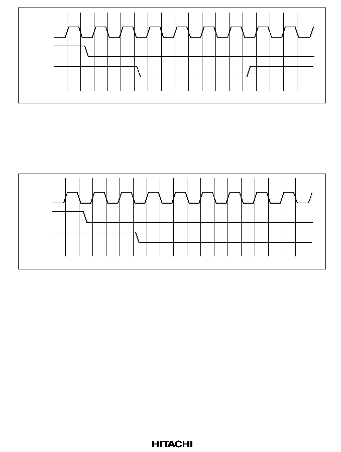
205
CKIO
BRLS
BGR
Bus request
Bus release
Refresh request
Figure 7.49 Case in Which
BGR is Negated
Case in Which
BGR is Not Negated: If access processing for an external device has been
initiated before the refresh request is generated, and the device is waiting to acquire the bus, the
BGR signal will not be negated. After the BRLS signal is negated, refreshing begins after
completion of the access involving the external device that was waiting for the bus.
CKIO
BRLS
BGR
Bus request
Bus release
Refresh request
Figure 7.50 Case in Which
BGR is Not Negated
When the SH7604 is being used in slave mode, the bus is released as soon as the bus access cycle
ends, but in the case of a slave designed by the user, multiple consecutive bus accesses may be
attempted in order to reduce the arbitration overhead. To ensure dependable refreshing in this case,
the design should provide for the bus to be released to prevent the slave holding the bus for longer
than the refresh cycle.
7.10.2
Slave Mode
In slave mode, the bus is usually released. External devices cannot be accessed unless the bus
arbitration sequence is performed to capture the bus. During a reset, the bus is released and the bus
arbitration sequence starts from the reset vector fetch.
The
BREQ signal is asserted (to low level) synchronously with the clock fall for capturing the bus.
The assertion of the
BACK signal (to low level) is sampled at the clock fall. When a BACK
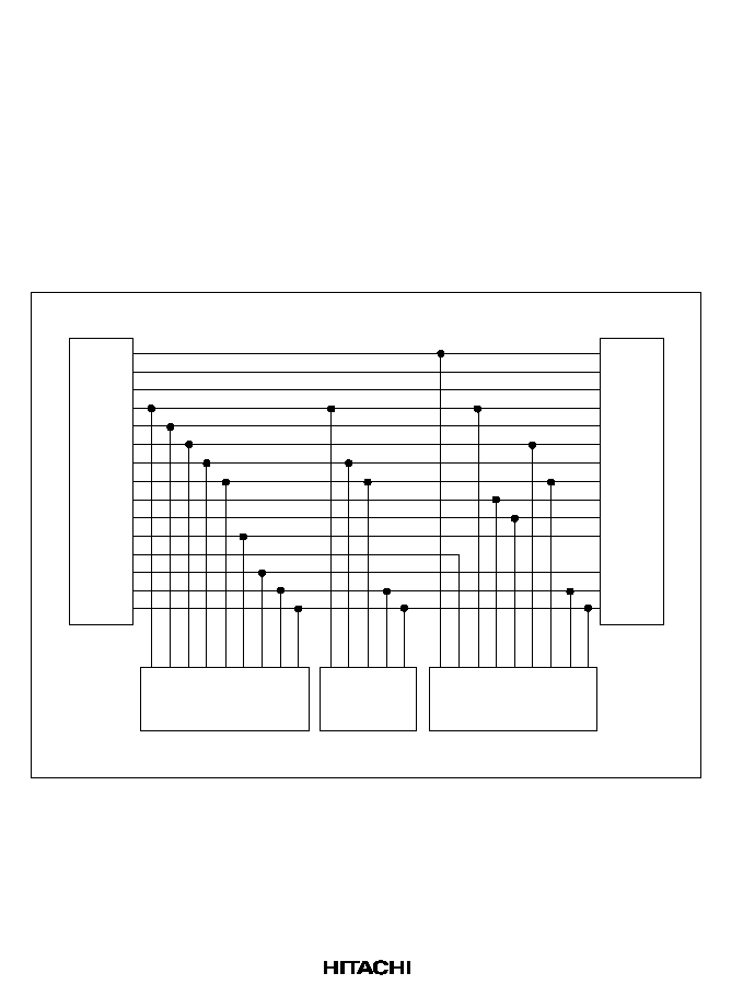
206
assertion is detected, the bus control signals are immediately driven at the negate level. Thereafter
the address and data bus drivers turn on at the following clock rise and the bus cycle starts. The
last signal negated when the access cycle ended is synchronized with the clock rise. Half a cycle
after the clock rise, the
BREQ signal is negated, the master notified that the bus is released, and
one cycle later the address and data output buffers turned off (high impedance). At the following
clock fall, the control signals become high impedance. Figure 7.48 shows the bus arbitration
timing for slave mode.
When the slave access cycle is for DRAM, synchronous DRAM or pseudo-SRAM, the bus is
released when the memory precharge finishes, just as for master mode. Since refresh control is
handled by the master mode device, any refresh control setting performed in the slave mode is
ignored. Figure 7.51 shows an example of master mode and slave mode connections.
CKIO
BRLS
BGR
CSn
BS
RD/
WR
RD
WEn
RAS
CAS
IVECF
CKE
WAIT
A26A0
D31D0
CS
BS
RD/
WR
RD
WEn
IVECF
WAIT
An
Dn
CS
OE
WEn
An
Dn
CK
CKE
CS
RAS
CAS
WE
DQMxx
An
Dn
CKIO
BREQ
BACK
CSn
BS
RD/
WR
RD
WEn
RAS
CAS
IVECF
CKE
WAIT
A26A0
D31D0
Interfaces with
other devices
SRAM
Synchronous DRAM
Slave
mode
Master
mode
Figure 7.51 Connection between Master and Slave Devices
7.10.3
Partial-Share Master Mode
In partial-share master mode, only the CS2 space is shared with other devices. Other CS spaces
can always be accessed. To set partial-share master mode, set to master mode using the external
mode pins and then set the PSHR bit in BCR to 1 in the power-on reset initialization procedure.

207
During a manual reset, the values of the bus state controller setting registers are held, so they do
not need to be set again.
Partial-share master mode is designed to be used with a chip in master mode. Figure 7.52 shows
an example of connections between a partial-share master mode and master mode SH7604. On the
master mode side, the CS3 space is connected to synchronous DRAM and the CS0 space to ROM.
On the partial-share master mode side, the CS0 space is connected to ROM, the master side
synchronous DRAM is connected to the CS2 space, and the CS3 space is connected to dedicated
synchronous DRAM. The partial-share master is also connected through the CS2 space to the
master synchronous DRAM so it can be accessed. The master, however, cannot access devices on
the partial-share master side. There is a buffer for addresses and control signals and a buffer for
data located between the partial-share master and the master. They are controlled by a buffer
control circuit. The buffers latch signals synchronous to the clock rise and match timing, so an AC
operating margin is assured. When the master side synchronous DRAM is read from the partial-
share master, however, address and control line output requires an extra cycle, and input of read
data requires an extra cycle. The CAS latency setting within the bus controller should be 2 higher
than the actual synchronous DRAM CAS latency. If the clock cycle is sufficiently long relative to
the time for addresses, control signals and write signals from the partial-share master to reach the
synchronous DRAM on the master side through the buffer and to the time for read data from the
synchronous DRAM on the master side to reach the partial-share master through the buffer, if the
respective setup time limits can be satisfied, then there is no need to delay by one cycle clock
signal synchronously with the clock. In this case, the previously described latch is not needed.
When a processor in the partial-share master mode accesses the CS2 space, it performs the
following procedure. The
BREQ signal is asserted at the clock fall to request the bus from the
master. The
BACK signal is sampled at every clock fall, and when an assertion is received, the
access cycle starts at the next clock rise. After the access ends,
BREQ is negated at the clock fall.
Control of the buffer when a CS2 space device is being accessed from the partial-share master
references the
BREQ and BACK signals. Notification that the bus is enabled for use is conducted
by the
BACK connected to the partial-share master, but the BACK signal may be negated while
the bus is in use when the master requires the bus back to service a refresh or the like. For this
reason, the
BREQ signal must be monitored to see whether the partial-share master can continue
using the bus after
BACK is asserted. For address buffers, after the address buffer is turned on by
the detection of a
BACK assertion, the buffer remains on until BREQ is negated. When BREQ is
negated, the buffer goes off. When the buffer is slow going off and it conflicts with the start of the
access cycle at the master, the
BREQ signal output from the partial-share master as part of the
buffer control circuit must be delayed a clock and input to the
BRLS signal.
When the bus is released after the CS2 space is accessed in partial-share master mode, the bus will
be released after waiting for the time required for auto-precharge if the CS2 space was
synchronous DRAM. Other spaces always have the bus themselves, so there is no precharge of
CS3 space memory upon release after a CS2 space bus request, even when DRAM, synchronous
DRAM or pseudo-SRAM is connected to the CS3 space. Partial-share master mode does not
refresh CS2 (it is ignored).
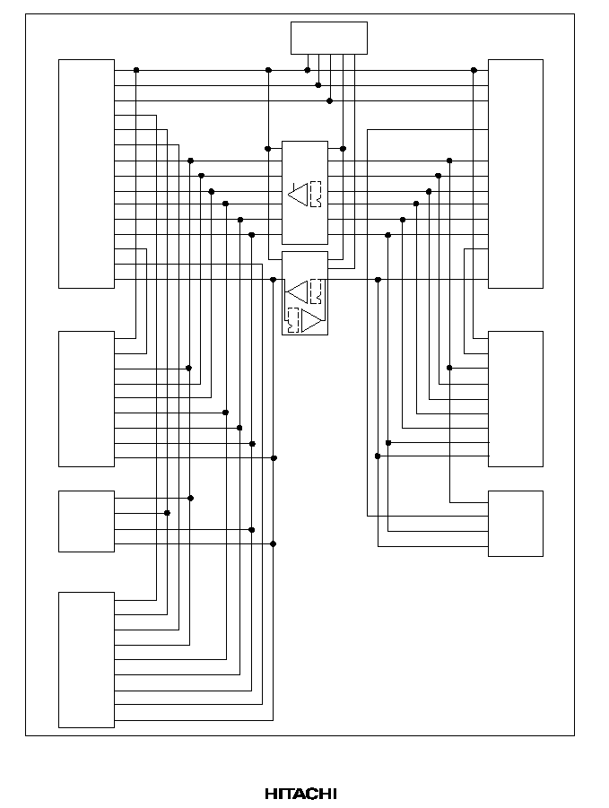
208
ROM
Master
mode
Synchronous
DRAM
ROM
Partial-share
master mode
Synchronous
DRAM
Interfaces with
other devices
Buffer
control
CK EN
CK EN
DIR
CKIO
BRLS
BGR
BS
RD
IVECF
CSn
RAS
CAS
RD/
WR
WEn
A26A0
CKE
WAIT
D31D0
CK
CKE
CS
RAS
CAS
WE
DQMxx
An
Dn
CS
OE
An
Dn
BS
RD
IVECF
CS
RD/
WEn
WEn
An
WAIT
Dn
CS
OE
An
Dn
CK
CKE
CS
RAS
CAS
WE
DQMxx
An
Dn
CKIO
BREQ
BACK
BS
RD
IVECF
CSn
RAS
CAS
RD/
WR
WEn
A26A0
CKE
WAIT
D31D0
Figure 7.52 Connection between Master and Partial-Share Master Devices

209
7.10.4
External Bus Address Monitor
The master and slave modes have a function to generate break interrupts and monitor the external
bus access cycle using the user break controller. The bus cycle is monitored by sampling the
external bus every time the clock rises while the bus is released. If the
BS signal is found to be
asserted (low level) when sampling is performed, the address at that time (A26A0) and read/write
signal RD/
WR are fetched and compared as the access address and access type (read or write).
When an external device has captured the bus and the DRAM or synchronous DRAM is in an
access cycle, the following points are important to make the address monitor function correctly.
BS goes low in the DRAM or synchronous DRAM access cycle in synchronization with the cycle
that outputs the column address. Because only the address of the cycle in which the
BS signal is
low is fetched and compared, even access to memories like these that multiplex addresses requires
outputting of the row address in the upper address bits. One of the bits of the address signal in the
column address output cycle in synchronous DRAM is used to specify the bank address, while the
other bit is used to specify whether to perform an auto-precharge. These always cause breaks on
the compared address, so mask these two bits when setting the comparison address. The masked
bit position is described in the section 7.5.2, Address Multiplexing.
7.10.5
Master/Slave Coordination
Roles must be shared between the master and slave to control system resources without
contradictions. DRAM, synchronous DRAM and pseudo-SRAM must be initialized before use.
When using standby operation to lower power consumption, the load must also be shared.
This SH7604 was designed with the idea that the master mode device would handle all controls,
such as initialization, refreshing, and standby control. When a 2-processor structure of connected
master and slave is used, all processing except for direct accesses to memory is controlled by the
master. When master mode is combined with partial-share master mode, the partial-share master
mode processor handles initialization, refreshing, and standby control for all CS spaces connected
to it except for the CS2 space. The master initializes memory connected directly to it.
The hardware or software sequence should be designed so that there are no slave-side processor
accesses until memory that requires initialization before use such as DRAM, synchronous DRAM
and pseudo-SRAM has completed its initialization. One method is to install an external circuit that
clears slave resets from the master. Another is to have the master write a flag when initialization is
complete to an SRAM or the like that does not require initialization, and then not to start access
until this flag is acknowledged by the slave. A third method is to install an external circuit that can
send an interrupt from master to slave and clear the slave's standby state with an interrupt from the
master to the slave when initialization ends.
In standby mode or the like when synchronous DRAM and pseudo-SRAM are in self-refresh
mode, memory is not precharged until the mode is cleared, so the master cannot release the bus.
The design should provide for the master to put the slave to sleep before self-refresh mode starts

210
or otherwise prevent the slave access cycle from starting, which prevents the slave from producing
a bus release request. The slave accesses these types of memories after the master finishes any
processing necessary when the self-refresh mode is cleared, such as refresh settings.
7.11
Other Topics
7.11.1
Resets
The bus state controller is completely initialized only in a power-on reset. All signals are
immediately negated, regardless of where in the bus cycle the SH7604 is, and the output buffer is
turned off if the bus arbitration mode is slave. Signal negation is simultaneous with turning the
output buffer off. All control registers are initialized. In standby mode, sleep mode, and a manual
reset, no bus state controller control registers are initialized. When a manual reset is performed,
any executing bus cycles are completed, and then the SH7604 waits for an access. When a cache
fill or 16-byte DMAC transfer is executing, the CPU or DMAC that is the bus master ends the
access in a longword unit, since the access request is canceled by the manual reset. This means
that when a manual reset is executed during a cache fill, the cache contents can no longer be
guaranteed. During a manual reset, the RTCNT does not count up, so no refresh request is
generated, and a refresh cycle is not initiated. To preserve the data of the DRAM, synchronous
DRAM or pseudo-SRAM, the pulse width of the manual reset must be shorter than the refresh
interval. Master mode chips accept arbitration requests even when a manual reset signal is
asserted. When a reset is executed only for the chip in master mode while the bus is released, the
BGR signal is negated to indicate this. If the BRLS signal is continuously asserted, the bus release
state is maintained.
7.11.2
Access as Seen from the CPU or DMAC
The SH7604 is internally divided into three buses: cache, internal, and peripheral. The CPU and
cache memory are connected to the cache bus, the DMAC and bus state controller are connected
to the internal bus, and the low-speed peripherals and mode registers are connected to the
peripheral bus. The user break controller is connected to both the cache bus and the internal bus.
The internal bus can be accessed from the cache bus, but not the other way around. The peripheral
bus can be accessed from the internal bus, but not the other way around. This results in the
following.
Data cannot be written from the DMAC to cache memory. When the DMAC causes a write to
memory, the contents of memory and the cache contents will be different. To rewrite the contents
of memory, the cache memory must be purged by software if the possibility exists that the data for
that address exists in the cache.

211
When the CPU starts a read access to a cache area, it first takes a cycle to find the cache. If there is
data in the cache, it fetches it and completes the access. If there is no data in the cache, a cache
data fill is performed via the internal bus, so four consecutive longword reads occur. For misses
that occur when byte or word operands are accessed or branches occur to odd word boundaries (4n
+ 2 addresses), filling is always performed by longword accesses on the chip-external interface. In
the cache-through area, the access is to the actual access address. When the access is an instruction
fetch, the access size is always longword.
For cache-through areas and on-chip peripheral module read cycles, after an extra cycle is added
to determine the cycle, the read cycle is started through the internal bus. Read data is sent to the
CPU through the cache bus.
When word write cycles access the cache area, the cache is searched. When the data of the
relevant address is found, it is written here. In parallel to this, the actual writing occurs through the
internal bus. When the right to use the internal bus is held, the CPU is notified that the write is
completed without waiting for the actual writing to the on-chip peripheral module or off the chip
to end. When the right to use the internal bus is not held, as when it is being used by the DMAC or
the like, there is a wait until the bus is acquired before the CPU is notified of completion.
Accesses to cache-through areas and on-chip peripheral modules work the same as in the cache
area, except for the cache search and write.
Because the bus state controller has one level of write buffer, the internal bus can be used for
another access even when the chip-external bus cycle has not ended. After a write has been
performed to low-speed memory off the chip, performing a read or write with an on-chip
peripheral module enables an access to the on-chip peripheral module without having to wait for
the completion of the write to low-speed memory.
During reads, the CPU always has to wait for the end of the operation. To immediately continue
processing after checking that the write to the device of actual data has ended, perform a dummy
read access to the same address consecutively to check that the write has ended.
The bus state controller's write buffer functions in the same way during accesses from the DMAC.
A dual-address DMA transfer thus starts in the next read cycle without waiting for the end of the
write cycle. When both the source address and destination address of the DMA are external spaces
to the chip, however, it must wait until the completion of the previous write cycle before starting
the next read cycle.

212
7.11.3
Emulator
When using the SH7604's emulator, operation differs from real chip operation in the following
ways.
To get trace data with the emulator, all accesses performed by the CPU and DMAC must be output
externally. It is not possible to completely analyze program execution or the contents of the data
accessed with only traces of access cycles performed exterior to the chip.
Reads of the cache from the CPU can be performed using only the cache bus, but the access
address and data read must be able to use the internal bus and external bus to be output externally.
The external bus is not needed to access on-chip peripheral modules with the CPU or DMAC, but
it is needed to output trace data. This means that when the emulator is used in the trace data fetch
mode, internal access operations of the CPU or DMAC are not performed in parallel with the
external bus cycle, so extra execution time is required compared to actual chips. Parallel execution
of accesses that follow writing to external destinations also should be executed after writing is
completed to carry out traces. To precisely measure the actual execution time, an actual chip rather
than an emulator should be used.
213
Section 8 Cache
8.1
Introduction
64
entries
Internal
data bus
Internal
address bus
Tag address
match signal
Cache
data bus
Way 0
Way 1
Way 2
Way 3
Cache
address bus
Cache data array
Cache address array
Tag
address
LRU
information
Data (16 bytes/line)
V
V: Valid bit
Figure 8.1 Cache Configuration
The SH7604 incorporates 4 kbytes of 4-way cache memory of mixed instruction/data type. The
SH7604 can also be used as 2-kbyte RAM and 2-kbyte cache memory (mixed instruction/data
type) by a setting in the cache control register CCR (two-way cache mode). CCR can specify that
either instructions or data do not use cache.
Each line of cache memory consists of 16 bytes. Cache memory is always updated in line units.
Four 32-bit accesses are required to update a line. Since the number of entries is 64, the six bits
(A9 to A4) in each address determine the entry. A four-way set associative configuration is used,
so up to four different instructions/data can be stored in the cache even when entry addresses
match. To efficiently use four ways having the same entry address, replacement is provided based
on a pseudo-LRU (least-recently used) replacement algorithm.
214
31
28
9
3
3
19
6
4
0
Byte address
in line
Entry address
Tag address
Access space
specification address
Address
Figure 8.2 Address
8.2
Cache Control Register (CCR)
Table 8.1
Cache Control Register
Name
Abbrev.
R/W
Initial Value
Address
Cache control register
CCR
R/W
H'00
H'FFFFFE92
The cache control register (CCR) is used for cache control. CCR must be set and the cache must
be initialized before use.
Bit:
7
6
5
4
3
2
1
0
Bit name:
W1
W0
--
CP
TW
OD
ID
CE
Initial value:
0
0
0
0
0
0
0
0
R/W:
R/W
R/W
R
R/W
R/W
R/W
R/W
R/W
·
Bits 7 and 6--Way Specification (W1 to W0): W1 and W0 specify the way when an address
array is directly accessed by address specification.
Bit 7: W1
Bit 6: W0
Description
0
0
Way 0
(Initial value)
1
Way 1
1
0
Way 2
1
Way 3
·
Bit 5--Reserved: This bit always reads 0. The write value should always be 0.
·
Bit 4--Cache Purge (CP): CP is a cache purge bit. When 1 is written to CP, all cache entries
and all valid bits and LRU bits of the way are initialized to 0. After initialization is complete,
the CP bit reverts to 0. The CP bit always reads 0.

215
Bit 4: CP
Description
0
Normal operation
(Initial value)
1
Cache purge
Note:
Always read 0.
·
Bit 3--Two-Way Mode (TW): TW is the two-way mode bit. The cache operates as a four-way
set associative cache when TW is 0 and as a two-way set associative cache and 2-kbyte RAM
when TW is 1. In the two-way mode, ways 2 and 3 are cache and ways 0 and 1 are RAM.
Ways 0 and 1 are read or written by direct access of the data array according to address space
specification.
Bit 3: TW
Description
0
Four-way mode
(Initial value)
1
Two-way mode
·
Bit 2--Data Replacement Disable (OD): OD is the bit for disabling data replacement. When
this bit is 1, data fetched from external memory is not written to the cache even if there is a
cache miss. Cache data is, however, read or updated during cache hits. OD is valid only when
CE is 1.
Bit 2: OD
Description
0
Normal operation
(Initial value)
1
Data not replaced even when cache miss occurs in data access
·
Bit 1--Instruction Replacement Disable (ID): ID is the bit for disabling instruction
replacement. When this bit is 1, an instruction fetched from external memory is not written to
the cache even if there is a cache miss. Cache data is, however, read or updated during cache
hits. ID is valid only when CE is 1.
Bit 1: ID
Description
0
Normal operation
(Initial value)
1
Data not replaced even when cache miss occurs in instruction fetch
·
Bit 0--Cache Enable (CE): CE is the cache enable bit. Cache can be used when CE is set to 1.
Bit 0: CE
Description
0
Cache disabled
(Initial value)
1
Cache enabled

216
8.3
Address Space and the Cache
The address space is divided into six partitions. The cache access operation is specified by
addresses. Table 8.2 lists the partitions and their cache operations. For more information on
address spaces, see section 7, Bus State Controller. Note that the spaces of the cache area and
cache-through area are the same.
Table 8.2
Address Space and Cache Operation
Addresses
A31A29
Partition
Cache Operation
000
Cache area
Cache is used when the CE bit in CCR is 1.
001
Cache-through area
Cache is not used.
010
Associative purge area
Cache line of the specified address is purged
(disabled).
011
Address array read/write area Cache address array is accessed directly.
110
Data array read/write area
Cache data array is accessed directly.
111
I/O area
Cache is not used.
8.4
Cache Operation
8.4.1
Cache Reads
This section describes cache operation when the cache is enabled and data is read from the CPU.
One of the 64 entries is selected by the entry address part of the address output from the CPU on
the cache address bus. The tag addresses of ways 0 through 3 are compared to the tag address parts
of the addresses output from the CPU. A match to the tag address of a way is called a cache hit. In
proper use, the tag addresses of each way differ from each other, and the tag address of only one
way will match. When none of the way tag addresses match, it is called a cache miss. Tag
addresses of entries with valid bits of 0 will not match in any case.
When a cache hit occurs, data is read from the data array of the way that was matched according to
the entry address, the byte address within the line, and the access data size. The data is then sent to
the CPU. The address output on the cache address bus is calculated in the CPU's instruction
execution phase and the results of the read are written during the CPU's write-back stage. The
cache address bus and cache data bus both operate as pipelines in concert with the CPU's pipeline
structure. From address comparison to data read requires 1 cycle; since the address and data
operate as a pipeline, consecutive reads can be performed at each cycle with no waits.
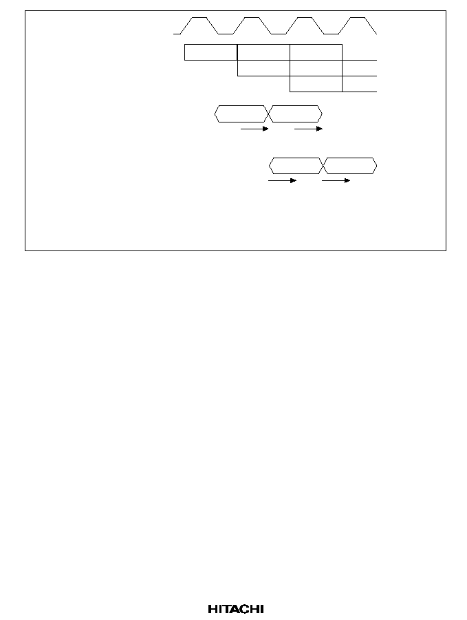
217
EX
CPU pipeline stage
Cache address bus
Cache data bus
MA
WB
EX
Address A
Cache tag comparison
Address B
MA
EX
Address A
Data array read
Address B
EX: Instruction execution
MA: Memory access
WB: Write-back
Figure 8.3 Read Access in Case of a Cache Hit
When a cache miss occurs, the way for replacement is determined using the LRU information, and
the read address from the CPU is written in the address array for that way. Simultaneously, the
valid bit is set to 1. Since the 16 bytes of data for replacing the data array are simultaneously read,
the address on the cache address bus is output to the internal address bus and 4 longwords are read
consecutively. Access starts with whatever address output to the internal address bus will make the
longword that contains the address to be read from the cache come last as the byte address within
the line as the order + 4. The data read on the internal data bus is written sequentially to the cache
data array. When the last data is written to the cache data array, it is simultaneously written to the
cache data bus and the read data is sent to the CPU.
The internal address bus and internal data bus also function as pipelines, just like the cache bus.
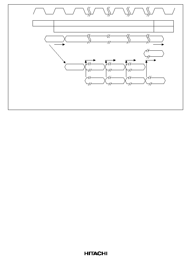
218
Data array write
Cache tag comparison
Cache tag comparison
EX
CPU
pipeline
stage
Cache
address
bus
Cache
data bus
Internal
address
bus
Internal
data bus
MA
WB
EX
MA
Address A
Address A + 4
Address B
Address A + 12
Address A + 8
Address A + 8
Address A + 4
Address A
Address A + 12
Address A
Address A
EX: Instruction execution
MA: Memory access
WB: Write-back
Figure 8.4 Read Access in Case of a Cache Miss
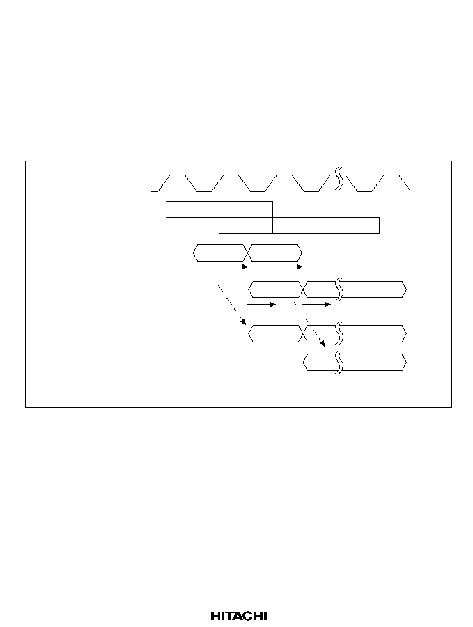
219
8.4.2
Write Access
This cache is of the write-through type, and writing to external memory is performed regardless of
whether or not there is a cache hit. The write address output to the cache address bus is used to
compare to the tag address of the cache's address array. When they match, the write data output to
the cache data bus in the following cycle is written to the data array. When they do not match,
nothing is written to the cache data array. The write address is output to the internal address bus 1
cycle later than the cache address bus. The write data is similarly output to the internal data bus 1
cycle later than the cache data bus. The CPU waits until the writes onto the internal bus are
completed.
EX
CPU pipeline stage
Cache address bus
Cache data bus
Internal address bus
Internal data bus
MA
EX
Address A
Cache tag comparison
Address B
MA
Address A
Address B
Address A
Address B
Address A
Data array write
EX: Instruction execution
MA: Memory access
Figure 8.5 Write Access
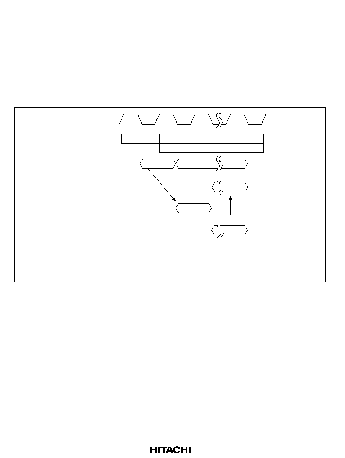
220
8.4.3
Cache-Through Access
When reading or writing a cache-through area, the cache is not accessed. Instead, the cache
address value is output to the internal address bus. For read operations, the read data output to the
internal address bus is fetched and output to the cache data bus. The read of the cache-through area
is only performed on the address in question. For write operations, the write data on the cache data
bus is output to the internal data bus. Writes on the cache through area are compared to the address
tag; except for the fact that nothing is written to the data array, the operation is the same as the
write shown in figure 8.5.
EX
CPU
pipeline stage
Cache
address bus
Cache
data bus
Internal
address bus
Internal
data bus
MA
WB
EX
MA
Address A
Address A
Address B
Address A
Address A
EX: Instruction execution
MA: Memory access
WB: Write-back
Figure 8.6 Reading Cache-Through Areas
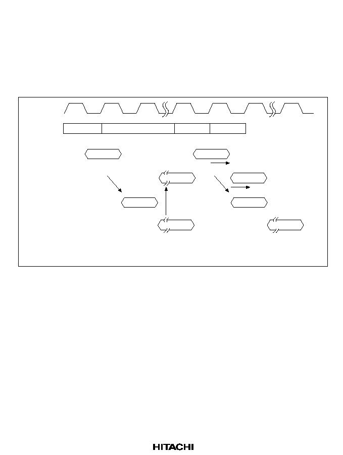
221
8.4.4
The TAS Instruction
The TAS instruction reads data from memory, compares it to 0, and reflects the result in the T bit
of the status register while setting the most significant bit to 1. It is an address for writing to the
same address. Reads from memory become cache-through operations even when the cache area is
accessed. Address tags are not compared. The updated value is written to memory through the
internal data bus, but before that the address tag is compared and if there are any matching entries,
a write is performed to the corresponding data array.
Data array write
Cache tag comparison
EX
CPU
pipeline
stage
Cache
address
bus
Cache
data bus
Internal
address
bus
Internal
data bus
MA
EX
MA
Address A
Address A'
Address A
Address A
Address A'
Address A'
Address A'
Address A
EX: Instruction execution
MA: Memory access
Figure 8.7 TAS Instruction Execution and the Cache

222
8.4.5
Pseudo-LRU and Cache Replacement
When a cache miss occurs during a read, the data of the missed address is read from 1 line (16
bytes) of memory and replaced. This makes it important to decide which of the ways to replace. It
is likely that the way least recently used has the highest probability of being the next to be
accessed. This algorithm for replacing ways is called the least recently used replacement
algorithm, or LRU. The hardware to implement it, however, is complex. For that reason, this
cache uses a pseudo-LRU replacement algorithm that keeps track of the order of way access and
replaces the oldest way.
Six bits of data are used as the LRU information. The bits indicate the access order for 2 ways, as
shown in figure 8.8. When the value is 1, access occurred in the direction of the appropriate arrow
in the figure. The direction of the arrow can be determined by reading the bit. All the arrows show
the oldest access toward that way, which becomes the object of replacement. The access order is
recorded in the LRU information bits, so the LRU information is rewritten when a cache hit occurs
during a read, when a cache hit occurs during a write, and when replacement occurs after a cache
miss. Table 8.3 shows the rewrite values; table 8.4 shows how ways are selected for replacement.
After a cache purge by CCR's CP bit, the LRU information is completely zeroized, so the initial
order used is way 3
way 2
way 1
way 0. Thereafter the way is selected according to the
order of access set by the program. Since the replacement will not be correct if the LRU gets an
inappropriate value, the address array write function can be used to rewrite. When this is done, be
sure not to write a value other than 0 as the LRU information.
When CCR's OD bit or ID bit is 1, neither will replace the cache even if a cache miss occurs
during data read or instruction fetch. Instead of replacing, the missed address data is read and
directly transferred to the CPU.
The two-way mode of the cache set by CCR's TW bit can only be implemented by replacing ways
2 and 3. Comparisons of tag addresses of address arrays are carried out on all four ways even in
two-way mode, so the valid bit of ways 1 and 0 must be zeroized prior to operation in the two-way
mode.
Writing for the tag address and valid bit for cache replacement does not wait for the read from
memory to be completed. When the memory access is aborted by a reset during replacement or the
like, the cache contents and memory contents may be out of sync, so always perform a purge.
223
Way 0
Way 2
Way 1
Way 3
Bit 5
Bit 2
Bit 3
Bit 4
Bit 1
Bit 0
Figure 8.8 LRU Information and Access Sequence
Table 8.3
LRU Information after Update
Bit 5
Bit 4
Bit 3
Bit 2
Bit 1
Bit 0
Way 0
0
0
0
--
--
--
Way 1
1
--
--
0
0
--
Way 2
--
1
--
1
--
0
Way 3
--
--
1
--
1
1
--: Holds the value before update.
Table 8.4
Selection Conditions for Replaced Way
Bit 5
Bit 4
Bit 3
Bit 2
Bit 1
Bit 0
Way 0
1
1
1
--
--
--
Way 1
0
--
--
1
1
--
Way 2
--
0
--
0
--
1
Way 3
--
--
0
--
0
0
--: Don't care.

224
8.4.6
Cache Initialization
Purges of the entire cache area can only be carried out by writing 0 to the CP bit in CCR. Writing
1 to the CP bit initializes the valid bit of the address array and all bits of the LRU information to 0.
Cache purges are completed in 1 cycle, but additional time is required for writing to CCR. Always
initialize the valid bit and LRU before enabling the cache.
When the cache is enabled, instruction reads are performed from the cache even during writing to
CCR. This means that the prefetched instructions are read from the cache. To do a proper purge,
write 0 to CCR's CE bit, then disable the cache and purge. Since CCR's CE bit is cleared to 0 by a
power-on reset or manual reset, the cache can be purged immediately by a reset.
8.4.7
Associative Purges
Associative purges invalidate 1 line (16 bytes) corresponding to specific address contents when
the contents are in the cache. When the contents of shared addresses are rewritten by one CPU in a
multiprocessor configuration, the other CPU cache must be invalidated if it also contains the
address. When writing is performed to the address found by adding H'40000000 to the purged
address, the valid bit of the entry storing the address prior to the addition is initialized to 0. 16
bytes are purged in each write, so a purge of 256 bytes of consecutive areas can be accomplished
in 16 writes. Access sizes when associative purges are performed should be longword. A purge of
1 line requires 2 cycles.
Associative purge:
Tag address
010
Address
Entry
address
--
31
9
3
0
19
6
3
4
28
Figure 8.9 Associative Purge Access
8.4.8
Data Array Access
The cache data array can be read or written directly via the data array read/write area. The access
sizes for the data array may be byte, word or longword. Data array accesses are completed in 1
cycle for both reads and writes. Since only the cache bus is used, the operation can proceed in
parallel even when another master, such as the DMAC, is using the bus. The data array of way 0 is
mapped on H'C0000000 to H'C00003FF, way 1 on H'C0000400 to H'C00007FF, way 2 on
H'C0000800 to H'C0000BFF and way 3 on H'C0000C00 to H'C0000FFF. When the two-way
mode is being used, the area H'C0000000 to H'C00007FF is accessed as 2 kbytes of on-chip
RAM. When the cache is disabled, the area H'C0000000 to H'C0000FFF can be used as 4 kbytes
of on-chip RAM.
225
When the contents of the way being used as cache is rewritten using a data array access, the
contents of external memory and cache will not match, so this method should be avoided.
Tag address
110
Address
Entry
address
BA
W
31
28
9
3
0
19
Data
31
0
32
6
3
4
Data
Data array read/write:
BA: Byte address within line
W: Way specification
Figure 8.10 Data Array Access
8.4.9
Address Array Access
The address array of the cache can be accessed so that the contents fetched to the cache can be
checked for purposes of program debugging or the like. The address array is mapped on
H'60000000 to H'600003FF. Since all of the ways are mapped to the same addresses, ways are
selected by rewriting the W1 and W0 bits in CCR. The address array can only be accessed in
longwords.
When the address array is read, the tag address, LRU information, and valid bit are output as data.
When the address array is written to, the tag address and valid bit are written from the cache
address bus. This requires that the write address be calculated according to the value to be written,
then written. LRU information is written from data, but 0 should always be written to prevent
malfunctions.
226
--
011
Address
Entry
address
--
31
28
9
3
0
19
6
3
4
Tag address
--
Data
LRU
--
-- V
31
9
3 2
0
19
6
3
1 1 2
--
LRU
information
--
31
9
3
0
22
6
4
Data
Tag address
011
Address
Entry
address
--
-- V
31
28
9
19
6
3
1 1 2
Address array read:
Address array write:
1
3 2
0
1
28
V: Valid bit
Figure 8.11 Address Array Access
8.5
Cache Use
8.5.1
Initialization
Cache memory is not initialized in a reset. Therefore, the cache must be initialized by software
before use. Cache initialization clears (to 0) the address array valid bit and all LRU information.
The address array write function can be used to initialize each line, but it is simpler to initialize it
once by writing 1 to the CP bit in CCR. Figure 8.12 shows how to initialize the cache.
MOV.W #H'FE92, R1
MOV.B @R1, R0 ;
AND #H'FE, R0 ;
MOV.B #R0, @R1 ; Cache disable
OR #H'10, R0
MOV.B R0, @R1 ; Cache purge
OR #H'01, R0
MOV.B R0, R1 ; Cache enable
Figure 8.12 Cache Initialization

227
8.5.2
Purge of Specific Lines
Since the SH7604 has no snoop function (for monitoring data rewrites), specific lines of cache
must be purged when the contents of cache memory and external memory differ as a result of an
operation. For instance, when a DMA transfer is performed to the cache area, cache lines
corresponding to the rewritten address area must be purged. All entries of the cache can be purged
by setting the CP bit in CCR to 1. However, it is efficient to purge only specific lines if only a
limited number of entries are to be purged.
An associative purge is used to purge specific lines. Since cache lines are 16 bytes long, purges are
performed in a 16-byte units. The four ways are checked simultaneously, and only lines holding
data corresponding to specified addresses are purged. When addresses do not match, the data at
the specified address is not fetched to the cache, so no purge occurs.
; Purging 32 bytes from address R3
MOV.L #H'40000000, R0
XOR R1, R1
MOV.L R1, @(R0, R3)
ADD #16, R3
MOV.L R1, @(R0, R3)
Figure 8.13 Purging Specific Addresses
When it is troublesome to purge the cache after every DMA transfer, it is recommended that the
OD bit in CCR be set to 1 in advance. When the OD bit is 1, the cache operates as cache memory
only for instructions. However, when data is already fetched into cache memory, specific lines of
cache memory must be purged for DMA transfers.
8.5.3
Cache Data Coherency
The SH7604's cache memory does not have a snoop function. This means that when data is shared
with a bus master other than the CPU, software must be used to ensure the coherency of data. For
this purpose, the cache-through area can be used, the break function can be used in external bus
cycles, or a cache purge can be performed with program logic.
If the cache-through area is to be used, the data shared by the bus masters is placed in the cache-
through area. This makes it easy to maintain data coherency, since access of the cache-through
area does not fetch data into the cache. When the shared data is accessed repeatedly and the
frequency of data rewrites is low, a lower access speed can adversely affect performance.
To use the external bus cycle break function, the user break controller is used. Set the user break
controller to generate an interrupt when a write cycle is detected to any of the areas that have
shared data. The interrupt handling routine purges the cache. Since the cache is purged whenever a

228
rewrite is detected, data coherency can be maintained. When data that extends over multiple
words, such as a structure, is rewritten, however, interrupts are generated at the rewrites, which
can lower performance. This method is most appropriate for cases in which it is difficult to predict
and detect the timing of data updates and the update frequency is low.
To purge the cache using program logic, the data updates are detected by the program flow and the
cache is then purged. For example, if the program inputs data from a disk, whenever reading of a
unit (such as a sector) is completed, the buffer address used for reading or the entire cache is
purged, thereby maintaining coherency. When data is to be handled between two processors, only
flags to provide mutual notification of completion of data preparation or completion of a fetch are
placed in the cache-through area. The data actually transferred is placed in the cache area and the
cache is purged before the first data read to maintain the coherency of the data. When semaphores
are used as the means of communication, data coherency can be maintained even when the cache
is not purged by utilizing the TAS instruction. The TAS instruction is not read within the cache;
the external access is always direct. This means that data can be synchronized with other masters
when it is read.
When the update unit it is small, specific addresses can be purged, so only the relevant addresses
are purged. When the update unit is larger, it is faster to purge the entire cache rather than purging
all the addresses in order, and then read in the data previously existing in the cache again from
external memory.
8.5.4
Two-Way Cache Mode
The 4-kbyte cache can be used as 2-kbyte RAM and 2-kbyte mixed instruction/data cache memory
by setting the TW bit in CCR to 1. Ways 2 and 3 become cache, and ways 0 and 1 become RAM.
The cache and RAM are initialized by setting the CP bit in CCR to 1. The valid bit and LRU bits
are cleared to 0.
When the initial values of the LRU information are set to 0, ways 3 and 2 are initially used, in that
order. Ways 3 and 2 are subsequently selected for replacement as specified by the LRU
information. The conditions for updating the LRU information are the same as for four-way mode,
except that the number of ways is two.
When designated as 2-kbyte RAM, ways 0 and 1 are accessed by data array access. Figure 8.14
shows the address mapping.
229
H'C0000000
H'C00003FF
H'C0000400
H'C00007FF
Way 0
Way 1
H'00000000
H'FFFFFFFF
Figure 8.14 Address Mapping of 2-kbyte RAM in the Two-Way Mode
8.5.5
Usage Notes
Standby: Disable the cache before entering the standby mode for power-down operation. After
returning from power-down, initialize the cache before use.
Cache Control Register: Changing the contents of CCR also changes cache operation. The
SH7604 makes full use of pipeline operations, so it is difficult to synchronize access. For this
reason, change the contents of the cache control register while disabling the cache or after the
cache is disabled.

230

231
Section 9 Direct Memory Access Controller (DMAC)
9.1
Overview
The SH7604 includes a two-channel direct memory access controller (DMAC). The DMAC can
be used in place of the CPU to perform high-speed data transfers between external devices
equipped with DACK (transfer request acknowledge signal), external memories, memory-mapped
external devices, and on-chip peripheral modules (except for the DMAC, BSC and UBC). Using
the DMAC reduces the burden on the CPU and increases the operating efficiency of the chip as a
whole.
9.1.1
Features
The DMAC has the following features:
·
Number of channels: 2
·
Address space: 4 Gbytes in the architecture
·
Selectable data transfer unit: Byte, word (2 bytes), longword (4 bytes) or 16-byte unit (16-byte
transfers first perform four longword reads and then four longword writes)
·
Maximum transfer count: 16,777,216 (16M) transfers
·
With cache hits, CPU instruction processing and DMA operation can proceed in parallel
·
The maximum transfer rate for synchronous DRAM burst transfers is 38 Mbytes/sec (f = 28.7
MHz)
·
Single address mode transfers: Either the transfer source or transfer destination (peripheral
device) is accessed by a DACK signal (selectable) while the other is accessed by address. One
transfer unit of data is transferred in each bus cycle.
Devices that can be used in DMA transfer:
External devices with DACK and memory-mapped external devices (including external
memories)
·
Dual address mode transfers: Both the transfer source and transfer destination are accessed by
address. One transfer unit of data is transferred in two bus cycles.
Device combinations capable of transfer:
Two external memories
External memory and memory-mapped external devices
Two memory-mapped external devices
External memory and on-chip peripheral module (excluding the DMAC, BSC and UBC).
Memory-mapped external devices and on-chip peripheral modules (excluding the DMAC,
BSC and UBC)

232
Two on-chip peripheral modules (excluding the DMAC, BSC and UBC)
(access size permitted by a register of the peripheral module that is the transfer source or
destination)
·
Transfer requests
External requests (from DREQ pins. DREQ can be detected either by edge or by level, and
either active-low or active-high can be selected)
On-chip peripheral module requests (serial communication interface (SCI))
Auto-request (the transfer request is generated automatically within the DMAC)
·
Selectable bus modes: Cycle-steal mode or burst mode
·
Selectable channel priority levels: Fixed or round-robin mode
·
An interrupt request can be sent to the CPU when data transfer ends
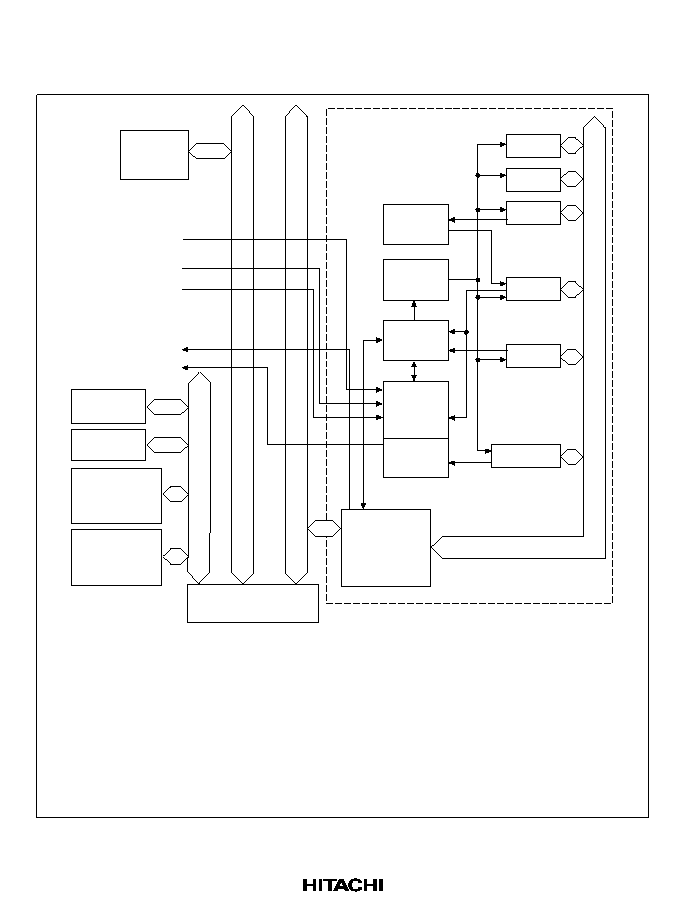
233
9.1.2
Block Diagram
Figure 9.1 shows a block diagram of the DMAC.
DREQn
RXI
TXI
DACKn
DEIn
DMAC
On-chip
peripheral
module
Peripheral bus
External bus
External
ROM
External
RAM
External I/O
(memory
mapped)
External I/O
(with
acknowledge)
Bus controller
Iteration
control
Register
control
Start-up
control
Request
priority
control
Interrupt
control
Bus interface
DMAC module bus
SARn
DARn
TCRn
CHCRn
DMAOR
VCRDMAn
Internal bus
DMAOR:
DMA operation register
SARn:
DMA source address register
DARn:
DMA destination address register
TCRn:
DMA transfer counter register
CHCRn:
DMA channel control register
VCRDMAn:
DMA vector register
DEIn:
DMA transfer end interrupt request to CPU
RXI:
On-chip SCI receive-data-full interrupt transfer request
TXI:
On-chip SCI transmit-data-full interrupt transfer request
n:
0 to 1
Figure 9.1 DMAC Block Diagram

234
9.1.3
Pin Configuration
Table 9.1 shows the DMAC pins.
Table 9.1
DMAC Pin Configuration
Channel
Name
Symbol
I/O
Function
0
DMA transfer request
DREQ0
I
DMA transfer request input from external
device to channel 0
DMA transfer request
acknowledge
DACK0
O
DMA transfer request acknowledge output
from channel 0 to external device
1
DMA transfer request
DREQ1
I
DMA transfer request input from external
device to channel 1
DMA transfer request
acknowledge
DACK1
O
DMA transfer request acknowledge output
from channel 1 to external device
9.1.4
Register Configuration
Table 9.2 summarizes the DMAC registers. The DMAC has a total of 13 registers. Each channel
has six control registers. One control register is shared by both channels.
235
Table 9.2
DMAC Registers
Channel Name
Abbr.
R/W
Initial
Value
Address
Access
Size
*3
0
DMA source address register 0
SAR0
R/W
Undefined
H'FFFFFF80 32
DMA destination address
register 0
DAR0
R/W
Undefined
H'FFFFFF84 32
DMA transfer count register 0
TCR0
R/W
Undefined
H'FFFFFF88 32
DMA channel control register 0
CHCR0
R/(W)
*1
H'00000000 H'FFFFFF8C 32
DMA vector number register N0 VCRDMA0 R/(W)
*1
Undefined
H'FFFFFFA0 32
DMA request/response selection
control register 0
DRCR0
R/(W)
*1
H'00
H'FFFFFE71 8
*3
1
DMA source address register 1
SAR1
R/W
Undefined
H'FFFFFF90 32
DMA destination address
register 1
DAR1
R/W
Undefined
H'FFFFFF94 32
DMA transfer count register 1
TCR1
R/W
Undefined
H'FFFFFF98 32
DMA channel control register 1
CHCR1
R/(W)
*1
H'00000000 H'FFFFFF9C 32
DMA vector number register N1 VCRDMA1 R/(W)
*1
Undefined
H'FFFFFFA8 32
DMA request/response selection
control register 1
DRCR1
R/(W)
*1
H'00
H'FFFFFE72 8
*3
Shared
DMA operation register
DMAOR
R/(W)
*2
H'00000000 H'FFFFFFB0 32
Notes: 1. Only 0 can be written to bit 1 of CHCR0 and CHCR1, after reading 1, to clear the flags.
2. Only 0 can be written to bits 1 and 2 of the DMAOR, after reading 1, to clear the flags.
3. Access DRCR0 and DRCR1 in byte units. Access all other registers in longword units.
9.2
Register Descriptions
9.2.1
DMA Source Address Registers 0 and 1 (SAR0 and SAR1)
Bit:
31
30
29
...
3
2
1
0
Bit name:
...
Initial value:
--
--
--
...
--
--
--
--
R/W:
R/W
R/W
R/W
...
R/W
R/W
R/W
R/W
DMA source address registers 0 and 1 (SAR0 and SAR1) are 32-bit read/write registers that
specify the source address of a DMA transfer. During a DMA transfer, these registers indicate the
next source address. (In single-address mode, SAR is ignored in transfers from external devices
with DACK to memory-mapped external devices or external memory). In 16-byte unit transfers,
always set the value of the source address to a 16-byte boundars (16n address). Operation results

236
cannot be guaranteed if other values are used. The value after a reset is undefined. Values are
retained in standby mode and during module standbys.
9.2.2
DMA Destination Address Registers 0 and 1 (DAR0 and DAR1)
Bit:
31
30
29
...
3
2
1
0
Bit name:
...
Initial value:
--
--
--
...
--
--
--
--
R/W:
R/W
R/W
R/W
...
R/W
R/W
R/W
R/W
DMA destination address registers 0 and 1 (DAR0 and DAR1) are 32-bit read/write registers that
specify the destination address of a DMA transfer. During a DMA transfer, these registers indicate
the next destination address. (In single-address mode, DAR is ignored in transfers from memory-
mapped external devices or external memory to external devices with DACK). The value after a
reset is undefined. Values are retained in standby mode and during module standbys.
9.2.3
DMA Transfer Count Registers 0 and 1 (TCR0 and TCR1)
Bit:
31
30
29
28
27
26
25
24
Bit name:
--
--
--
--
--
--
--
--
Initial value:
0
0
0
0
0
0
0
0
R/W:
R
R
R
R
R
R
R
R
Bit:
23
22
21
...
3
2
1
0
Bit name:
...
Initial value:
--
--
--
...
--
--
--
--
R/W:
R/W
R/W
R/W
...
R/W
R/W
R/W
R/W
DMA transfer count registers 0 and 1 (TCR0 and TCR1) are 32-bit read/write registers that
specify the DMA transfer count. The lower 24 of the 32 bits are valid. The value is written as 32
bits, including the upper eight bits. The number of transfers is 1 when the setting is H'00000001,
16,777,215 when the setting is H'00FFFFFF and 16, 777,216 (the maximum) when H'00000000 is
set. During a DMA transfer, these registers indicate the remaining transfer count.
Set the initial value as the write value in the upper eight bits. These bits always read 0. The initial
value after a reset is undefined. Values are retained in standby mode and during module standbys.
For 16-byte transfers, set the count to 4 times the number of transfers.

237
9.2.4
DMA Channel Control Registers 0 and 1 (CHCR0 and CHCR1)
Bit:
31
30
29
...
19
18
17
16
Bit name:
--
--
--
...
--
--
--
--
Initial value:
0
0
0
...
0
0
0
0
R/W:
R
R
R
...
R
R
R
R
Bit:
15
14
13
12
11
10
9
8
Bit name:
DM1
DM0
SM1
SM0
TS1
TS0
AR
AM
Initial value:
0
0
0
0
0
0
0
0
R/W:
R/W
R/W
R/W
R/W
R/W
R/W
R/W
R/W
Bit:
7
6
5
4
3
2
1
0
Bit name:
AL
DS
DL
TB
TA
IE
TE
DE
Initial value:
0
0
0
0
0
0
0
0
R/W:
R/W
R/W
R/W
R/W
R/W
R/W
R/(W)*
R/W
Note:
Only 0 can be written, to clear the flag.
DMA channel control registers 0 and 1 (CHCR0 and CHCR1) are 32-bit read/write registers that
control the DMA transfer mode. They also indicate the DMA transfer status. Only the lower 16 of
the 32 bits are valid. They are written as 32-bit values, including the upper 16 bits. Write the initial
values to the upper 16 bits. These bits always read 0. The registers are initialized to H'00000000
by a reset and in standby mode. Values are retained during a module standby.
·
Bits 15 and 14--Destination Address Mode Bits 1, 0 (DM1, DM0): Select whether the DMA
destination address is incremented, decremented or left fixed (in single address mode, DM1
and DM0 are ignored when transfers are made from a memory-mapped external device, on-
chip peripheral module, or external memory to an external device with DACK). DM1 and
DM0 are initialized to 00 by a reset and in standby mode. Values are retained during a module
standby.

238
Bit 15: DM1
Bit 14: DM0
Description
0
0
Fixed destination address
(Initial value)
1
Destination address is incremented (+1 for byte transfer size,
+2 for word transfer size, +4 for longword transfer size, +16
for 16-byte transfer size)
1
0
Destination address is decremented (1 for byte transfer size,
2 for word transfer size, 4 for longword transfer size, 16
for 16-byte transfer size)
1
Reserved (setting prohibited)
·
Bits 13 and 12--Source Address Mode Bits 1, 0 (SM1, SM0): Select whether the DMA source
address is incremented, decremented or left fixed. In single address mode, SM1 and SM0 are
ignored when transfers are made from an external device with DACK to a memory-mapped
external device, on-chip peripheral module, or external memory. For a 16-byte transfer, the
address is incremented by +16 regardless of the SM1 and SM0 values. SM1 and SM0 are
initialized to 00 by a reset and in standby mode. Values are retained during a module standby.
Bit 13: SM1
Bit 12: SM0
Description
0
0
Fixed source address (+16 for 16-byte transfer size)
(Initial value)
1
Source address is incremented (+1 for byte transfer size, +2
for word transfer size, +4 for longword transfer size, +16 for
16-byte transfer size)
1
0
Source address is decremented (1 for byte transfer size, 2
for word transfer size, 4 for longword transfer size, +16 for
16-byte transfer size)
1
Reserved (setting prohibited)
·
Bits 11 and 10--Transfer Size Bits (TS1, TS0): Select the DMA transfer size. When the
transfer source or destination is an on-chip peripheral module register for which an access size
has been specified, that size must be selected. During 16-byte transfers, set the transfer address
mode bit for dual address mode. TS1 and TS0 are initialized to 00 by a reset and in standby
mode. Values are retained during a module standby.
Bit 11: TS1
Bit 10: TS0
Description
0
0
Byte unit
(initial value)
1
Word (2-byte) unit
1
0
Longword (4-byte) unit
1
16-byte unit (4 longword transfers)

239
·
Bit 9--Auto Request Mode Bit (AR): Selects whether auto-request (generated within the
DMAC) or module request (an external request or from the on-chip SCI module) is used for
the transfer request. The AR bit is initialized to 0 by a reset and in standby mode. Its value is
retained during a module standby.
Bit 9: AR
Description
0
Module request mode
(Initial value)
1
Auto-request mode
·
Bit 8--Acknowledge/Transfer Mode Bit (AM): In dual address mode, this bit selects whether
the DACK signal is output during the data read cycle or write cycle. In single-address mode, it
selects whether to transfer data from memory to device or from device to memory. The AM bit
is initialized to 0 by a reset and in standby mode. Its value is retained during a module standby.
Bit 8: AM
Description
0
DACK output in read cycle/transfer from memory to device (Initial value)
1
DACK output in write cycle/transfer from device to memory
·
Bit 7--Acknowledge Level Bit (AL): Selects whether the DACK signal is an active-high
signal or an active-low signal. The AL bit is initialized to 0 by a reset and in standby mode. Its
value is retained during a module standby.
Bit 7: AL
Description
0
DACK is an active-low signal
(Initial value)
1
DACK is an active-high signal
·
Bit 6--DREQ Select Bit (DS): Selects the DREQ input detection method used. The DS bit is
initialized to 0 by a reset and in standby mode. Its value is retained during a module standby.
Bit 6: DS
Description
0
Detected by level
(Initial value)
1
Detected by edge
·
Bit 5--DREQ Level Bit (DL): Selects active-high or active-low for the DREQ signal. The DL
bit is initialized to 0 by a reset and in standby mode. Its value is retained during a module
standby.

240
Bit 5: DL
Description
0
When DS is 0, DREQ is detected by low level; when DS is 1, DREQ is
detected by fall
(Initial value)
1
When DS is 0, DREQ is detected by high level; when DS is 1, DREQ is
detected by rise
·
Bit 4--Transfer Bus Mode Bit (TB): Selects the bus mode for DMA transfers. The TB bit is
initialized to 0 by a reset and in standby mode. Its value is retained during a module standby.
Bit 4: TB
Description
0
Cycle-steal mode
(Initial value)
1
Burst mode
·
Bit 3--Transfer Address Mode Bit (TA): Selects the DMA transfer address mode. The TA bit
is initialized to 0 by a reset and in standby mode. Its value is retained during a module standby.
Bit 3: TA
Description
0
Dual address mode
(Initial value)
1
Single address mode
·
Bit 2--Interrupt Enable Bit (IE): Determines whether or not to request a CPU interrupt at the
end of a DMA transfer. When the IE bit is set to 1, an interrupt (DEI) request is setnt to the
CPU when the TE bit is set. The IE bit is initialized to 0 by a reset and in standby mode. Its
value is retained during a module standby.
Bit 2: IE
Description
0
Interrupt disabled
(Initial value)
1
Interrupt enabled
·
Bit 1--Transfer-End Flag Bit (TE): Indicates that the transfer has ended. When the value in the
DMA transfer count register (TCR) becomes 0, the DMA transfer ends normally and the TE
bit is set to 1. This flag is not set if the transfer ends because of an NMI interrupt or DMA
address error, or because the DME bit of the DMA operation register (DMAOR) or the DE bit
was cleared. To clear the TE bit, read 1 from it and then write 0. When the TE bit is set, setting
the DE bit to 1 will not enable a transfer. The TE bit is initialized to 0 by a reset and in standby
mode. Its value is retained during a module standby.
241
Bit 1: TE
Description
0
DMA has not ended or was aborted
(Initial value)
Cleared by reading 1 from the TE bit and then writing 0
1
DMA has ended normally (by TCR = 0)
·
Bit 0--DMA Enable Bit (DE): Enables or disables DMA transfers. In auto-request mode, the
transfer starts when this bit or the DME bit in DMAOR is set to 1. The NMIF and AE bits in
DMAOR and the TE bit must be all set to 0. In external request mode or on-chip peripheral
module request mode, the transfer begins when the DMA transfer request is received from the
relevant device or on-chip peripheral module, provided this bit and the DME bit are set to 1.
As with the auto-request mode, the TE bit and the NMIF and AE bits in DMAOR must be all
set to 0. The transfer can be stopped by clearing this bit to 0. The DE bit is initialized to 0 by a
reset and in standby mode. Its value is retained during a module standby.
Bit 0: DE
Description
0
DMA transfer disabled
(Initial value)
1
DMA transfer enabled
9.2.5
DMA Vector Number Registers 0 and 1 (VCRDMA0, VCRDMA1)
Bit:
31
30
29
...
11
10
9
8
Bit name:
--
--
--
...
--
--
--
--
Initial value:
0
0
0
...
0
0
0
0
R/W:
R
R
R
...
R
R
R
R
Bit:
7
6
5
4
3
2
1
0
Bit name:
VC7
VC6
VC5
VC4
VC3
VC2
VC1
VC0
Initial value:
--
--
--
--
--
--
--
--
R/W:
R/W
R/W
R/W
R/W
R/W
R/W
R/W
R/W
DMA vector number registers 0 and 1 (VCRDMA0, VCRDMA1) are 32-bit read/write registers
that set the DMAC transfer-end interrupt vector number. Only the lower eight bits of the 32 are
effective. They are written as 32-bit values, including the upper 24 bits. Write the initial values to
the upper 24 bits. These bits are initialized to H'000000XX (last eight bits are undefined) by a
reset and in standby mode. Values are retained during a module standby.
·
Bits 31 to 8--Reserved: These bits always read 0. The write value should always be 0.

242
·
Bits 7 to 0--Vector Number Bits 70 (VC7VC0): Set the interrupt vector numbers at the end
of a DMAC transfer. Interrupt vector numbers of 0127 can be set. When a transfer-end
interrupt occurs, exception handling and interrupt control fetch the vector number and control
is transferred to the specified interrupt handling routine. The VC7VC0 bits are undefined
upon reset and in standby mode. Always write 0 to VC7.
9.2.6
DMA Request/Response Selection Control Registers 0 and 1 (DRCR0, DRCR1)
Bit:
7
6
5
4
3
2
1
0
Bit name:
--
--
--
--
--
--
RS1
RS0
Initial value:
0
0
0
0
0
0
0
0
R/W:
R
R
R
R
R
R
R/W
R/W
DMA request/response selection control registers 0 and 1 (DRCR0, DRCR1) are 8-bit read/write
registers that set the vector address of the DMAC transfer request source. They are written as 8-bit
values. They are initialized to H'00 by a reset, but retain their values in a module standby.
·
Bits 7 to 2--Reserved
·
Bits 1 and 0--Resource Select Bits 1 and 0 (RS1, RS0): Specify which transfer request to input
to the DMAC. Changing the transfer request source must be done when the DMA enable bit
(DE) is 0. The RS1 and RS0 bits are initialized to 00 by a reset.
Bit 1: RS1
Bit 0: RS0
Description
0
0
DREQ (external request)
(Initial value)
0
1
RXI (on-chip SCI receive-data-full interrupt transfer request)*
1
0
TXI (on-chip SCI transmit-data-empty interrupt transfer
request)*
1
1
Reserved (setting prohibited)
Note:
For RX2 and TX1, set for dual transfer mode.
The DREQ settings in CHCR are DS = 1 and DL = 0.

243
9.2.7
DMA Operation Register (DMAOR)
Bit:
31
30
29
...
11
10
9
8
Bit name:
--
--
--
...
--
--
--
--
Initial value:
0
0
0
...
0
0
0
0
R/W:
R
R
R
...
R
R
R
R
Bit:
7
6
5
4
3
2
1
0
Bit name:
--
--
--
--
PR
AE
NMIF
DMIE
Initial value:
0
0
0
0
0
0
0
0
R/W:
R
R
R
R
R/W
R/(W)*
R/(W)*
R/W
Note:
Only 0 can be written, to clear the flag.
The DMA operation register (DMAOR) is a 32-bit read/write register that controls the DMA
transfer mode. It also indicates the DMA transfer status. Only the lower four of the 32 bits are
valid. DMAOR is written as a 32-bit value, including the upper 28 bits. Write the initial values to
the upper 28 bits. These bits always read 0. DMAOR is initialized to H'00000000 by a reset and in
standby mode.
·
Bits 31 to 4--Reserved: These bits always read 0. The write value should always be 0.
·
Bit 3--Priority Mode Bit (PR): Selects the priority level between channels when there are
transfer requests for multiple channels. It is initialized to 0 by a reset and in standby mode. Its
value is retained during a module standby.
Bit 3: PR
Description
0
Fixed priority (channel 0 > channel 1)
(Initial value)
1
Round-robin (Top priority shifts to bottom after each transfer. The
priority for the first DMA transfer after a reset is channel 1 > channel 0)
·
Bit 2--Address Error Flag Bit (AE): This flag indicates that an address error has occurred in
the DMAC. When the AE bit is set to 1, DMA transfer cannot be enabled even if the DE bit in
the DMA channel control register (CHCR) is set to 1. To clear the AE bit, read 1 from it and
then write 0. Operation is performed up to the DMAC transfer being executed when the
address error occurred. AE is initialized to 0 by a reset and in standby mode.
Bit 2: AE
Description
0
No DMAC address error
(Initial value)
To clear the AE bit, read 1 from it and then write 0
1
Address error by DMAC

244
·
Bit 1--NMI Flag Bit (NMIF): This flag indicates that an NMI interrupt has occurred. When
the NMIF bit is set to 1, DMA transfer cannot be enabled even if the DE bit in CHCR and the
DME bit are set to 1. To clear the NMIF bit, read 1 from it and then write 0. Ends after the
DMAC operation executing when the NMI comes in (operation goes to destination). When the
NMI interrupt is input while the DMAC is not operating, the NMIF bit is set to 1. The NMIF
bit is initialized to 0 by a reset or in the standby mode. Values are held during a module
standby.
Bit 1: NMIF
Description
0
No NMIF interrupt (initial value)
To clear the NMIF bit, read 1 from it and then write 0.
1
NMIF has occurred
·
Bit 0--DMA Master Enable Bit (DME): Enables or disables DMA transfers on all channels. A
DMA transfer becomes enabled when the DE bit in the CHCR and the DME bit are set to 1.
For this to be effective, however, the TE bit in CHCR and the NMIF and AE bits must all be 0.
When the DME bit is cleared, all channel DMA transfers are aborted. DME is initialized to 0
by a reset and in standby mode. Its value is retained during a module standby.
Bit 0: DME
Description
0
DMA transfers disabled on all channels
(Initial value)
1
DMA transfers enabled on all channels

245
9.3
Operation
When there is a DMA transfer request, the DMAC starts the transfer according to the
predetermined channel priority; when the transfer-end conditions are satisfied, it ends the transfer.
Transfers can be requested in three modes: auto-request, external request, and on-chip module
request. A transfer can be in either single address mode or dual address mode. The bus mode can
be either burst or cycle-steal.
9.3.1
DMA Transfer Flow
After the DMA source address registers (SAR), DMA destination address registers (DAR), DMA
transfer count registers (TCR), DMA channel control registers (CHCR), DMA vector number
registers (VCRDMA), DMA request/response selection control registers (DRCR), and DMA
operation register (DMAOR) are initialized (initializing sets each register so that ultimately the
condition (DE = 1, DME = 1, TE = 0, NMIF = 0, AE = 0) is satisfied), the DMAC transfers data
according to the following procedure:
1. Checks to see if transfer is enabled (DE = 1, DME = 1, TE = 0, NMIF = 0, AE = 0)
2. When a transfer request comes and transfer is enabled, the DMAC transfers 1 transfer unit of
data. (In auto-request mode, the transfer begins automatically when the DE bit and DME bit
are set to 1. The TCR value will be decremented by 1.) The actual transfer flows vary
depending on the address mode and bus mode.
3. When the specified number of transfers have been completed (when TCR reaches 0), the
transfer ends normally. If the IE bit in CHCR is set to 1 at this time, a DEI interrupt is sent to
the CPU.
4. When an address error occurs in the DMAC or an NMI interrupt is generated, the transfer is
aborted. Transfers are also aborted when the DE bit in CHCR or the DME bit in DMAOR is
changed to 0.
Figure 9.2 shows a flowchart illustrating this procedure.
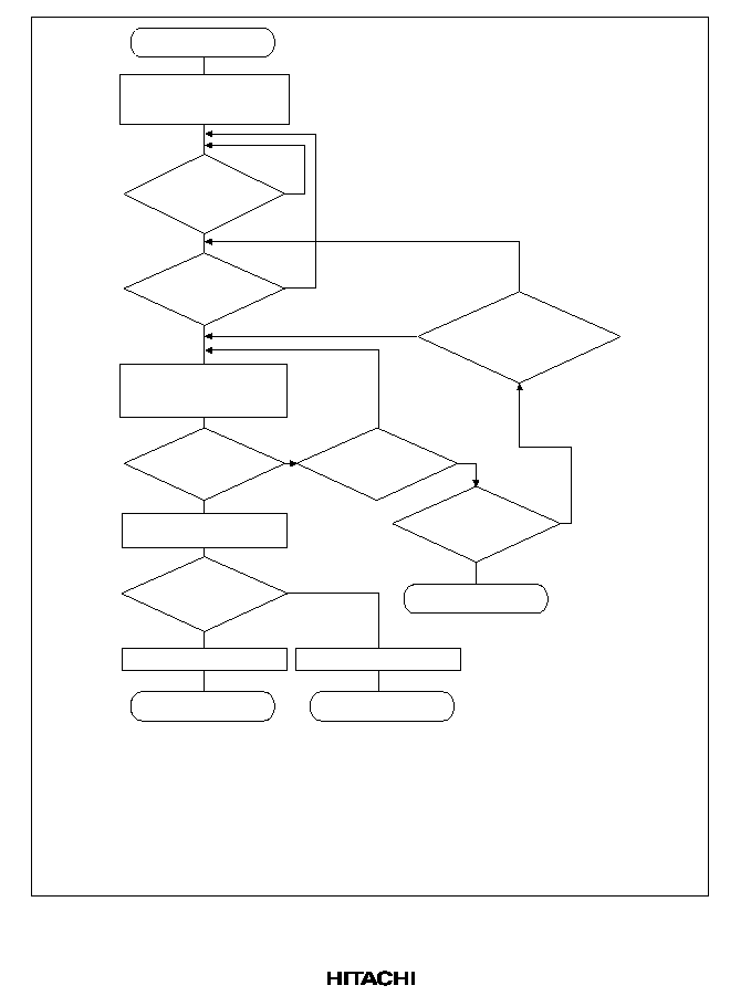
246
TCR = 0?
DE,
DME = 1 and NMIF,
AE, TE = 0?
Has a
transfer request been
generated?*
1
Transfer aborted
Initial settings
(SAR, DAR, TCR, CHCR,
VCRDMA, DRCR, DMAOR)
Transfer
TCR-1
TCR,
SAR, and DAR updated
DEI interrupt request
(when IE = 1)
TE = 1
TE = 1
No
Yes
No
Yes
No
Yes
No
Yes
No
*
3
*
5
*
4
*
2
Start
End normally
End transfer
Yes
16-byte transfer
in progress?
NMIF = 1 or
AE = 1, or DE = 0, or
DME = 0?
NMIF = 1,
or AE = 1, or DE = 0,
or DME
= 0?
Bus
mode, transfer
request mode, DREQ detec-
tion method?
Notes: 1. In auto-request mode, the transfer will start when the NMIF, AE, and TE bits are all 0
and the DE and DME bits are then set to 1.
2. In burst mode, DREQ = level detection (external request), or cycle-steal mode.
3. In burst mode, DREQ = edge detection (external request), or auto-request mode in
burst mode.
4. 16-byte transfer cycle in progress.
5. End of a 16-byte transfer cycle.
Figure 9.2 DMA Transfer Flow

247
9.3.2
DMA Transfer Requests
DMA transfer requests are usually generated in either the data transfer source or destination, but
they can also be generated by devices that are neither the source nor the destination. Transfers can
be requested in three modes: auto-request, external request, and on-chip peripheral module
request. The request mode is selected with the AR bit in DMA channel control registers 0 and 1
(CHCR0, CHCR1) and the RS0 and RS1 bits in DMA request/response selection control registers
0 and 1 (DRCR0, DRCR1).
Table 9.3
Selecting the DMA Transfer Request Using the AR and RS Bits
CHCR
DRCR
AR
RS1
RS0
Request Mode
Resource Select
0
0
0
Module request mode
DREQ external request (external request mode)
0
1
RXI (SCI receive) request
1
0
TXI (SCI transmit) request
1
X
X
Auto-request mode
Auto-Request: When there is no transfer request signal from an external source (as in a memory-
to-memory transfer or a transfer between memory and an on-chip peripheral module unable to
request a transfer), the auto-request mode allows the DMAC to automatically generate a transfer
request signal internally. When the DE bits in CHCR0 and CHCR1 and the DME bit in the DMA
operation register (DMAOR) are set to 1, the transfer begins (so long as the TE bits in CHCR0 and
CHCR1 and the NMIF and AE bits in DMAOR are all 0).
External Request: In this mode a transfer is started by a transfer request signal (DREQ) from an
external device. Choose one of the modes shown in table 9.4 according to the application system.
When DMA transfer is enabled (DE = 1, DME = 1, TE = 0, NMIF = 0, AE = 0), a transfer is
performed upon input of a DREQ signal.

248
Table 9.4
Selecting External Request Modes with the TA and AM Bits
CHCR
Transfer
TA
AM
Address Mode
Acknowledge Mode
Source
Destination
0
0
Dual address
mode
DACK output in read
cycle
Any*
1
Any*
1
1
Dual address
mode
DACK output in write
cycle
Any*
1
Any*
1
1
0
Single address
mode
Data transferred from
memory to device
External memory
*2
or memory-mapped
external device
External device
with DACK
1
Single address
mode
Data transferred from
device to memory
External device
with DACK
External memory
*2
or memory-mapped
external device
Notes: 1. External memory, memory-mapped external device, on-chip peripheral module
(excluding DMAC, BSC, and UBC)
2. Except synchronous DRAM
Choose to detect DREQ either by the falling edge or by level using the DS and DL bits in CHCR0
and CHCR1 (DS = 0 is level detection, DS = 1 is edge detection; for edge detection, DL = 0 is
rising edge, DL = 1 is falling edge; for level detection, DL = 0 is active-low, DL = 1 is active-
high). The source of the transfer request does not have to be the data transfer source or destination.
Table 9.5
Selecting the External Request Signal with the DS and DL Bits
DRCR
DS
DL
External Request
0
0
Level (active-low)
1
Level (active-high)
1
0
Edge (falling)
1
Edge (rising)
On-Chip Module Request: In this mode, transfers are started by the transfer request signal
(interrupt request signal) of an on-chip peripheral module in the SH7064. The transfer request
signals are the receive-data-full interrupt (RXI) and transmit-data-empty interrupt (TXI) of the
serial communication interface (SCI) (table 9.6). If DMA transfer is enabled (DE = 1, DME = 1,
TE = 0, NMIF = 0, AE = 0), DMA transfer starts upon the input of a transfer request signal.

249
When RXI (transfer request when the SCI's receive data buffer is full) is set as the transfer
request, however, the transfer source must be the SCI's receive data register (RDR). Likewise,
when TXI (transfer request when the SCI's transmit data buffer is empty) is set as the transfer
request, the transfer destination must be the SCI's transmit data register (TDR).
Table 9.6
Selecting On-Chip Peripheral Module Request Mode with the AR and RS bits
AR
RS1 RS0
DMA Transfer
Request
Source
DMA Transfer
Request Signal
Source
Destination
Bus
Mode
DREQ
Setting
0
0
1
SCI
receiver
RXI (SCI receive-
data-full transfer
request)
RDR
Any*
Cycle-
steal
Edge,
active-low
0
1
0
SCI
transmitter
TXI (SCI transmit-
data-empty transfer
request)
Any*
TDR
Cycle-
steal
Edge,
active-low
Note:
External memory, memory-mapped external device, on-chip peripheral module (excluding
DMAC, BSC, and UBC)
When outputting transfer requests from the SCI, its interrupt enable bits (TIE and RIE in SCR)
must be set to output the interrupt signals. Note that transfer request signals from on-chip
peripheral modules (interrupt request signals) are sent not just to the DMAC but to the CPU as
well. When an on-chip peripheral module is specified as the transfer request source, set the
priority level values in the interrupt priority level registers (IPRCIPRE) of the interrupt controller
(INTC) at or below the levels set in the I3I0 bits of the CPU's status register so that the CPU
does not accept the interrupt request signal.
The DMA transfer request signals shown in table 9.6 are automatically fetched when the
corresponding DMA transfer is performed. If cycle-steal mode is used, a DMA transfer request
(interrupt request) from any module will be cleared at the first transfer; if burst mode is used, it
will be cleared at the last transfer.
9.3.3
Channel Priorities
When the DMAC receives simultaneous transfer requests on two channels, it selects a channel
according to a predetermined priority order. There are two priority modes, fixed and round-robin.
The channel priority is selected by the priority bit, PR, in the DMA operation register (DMAOR).
Fixed Priority Mode: In this mode, the relative channel priority levels are fixed. When PR is set
to 0, the priority, high to low, is channel 0 > channel 1. Figure 9.3 shows an example of a transfer
in burst mode.
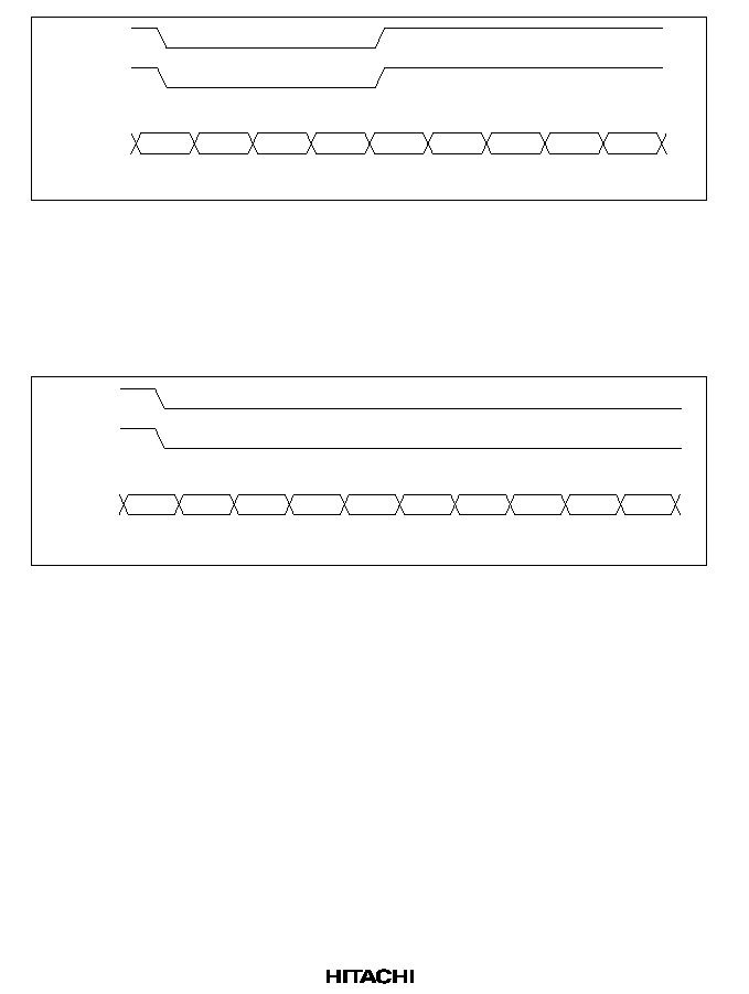
250
CPU
Bus
cycle
DREQ1
DREQ0
CPU
CPU
Channel 0
source
Channel 0
destination
Channel 0
source
Channel 0
destination
Channel 1
source
Channel 1
destination
Figure 9.3 Fixed Mode Burst DMA Transfer (Dual Address, Active-Low DREQ Level)
In cycle-steal mode, once a channel 0 request is accepted, channel 1 requests are also accepted
until the next request is made, which makes more effective use of the bus cycle. When requests
come simultaneously for channel 0 and channel 1 when DMA operation is starting, the first is
transmitted multiplexed with channel 0 and thereafter channel 1 and channel 0 transfers are
performed alternately.
CPU
Bus
cycle
DREQ1
DREQ0
CPU
CPU
CPU
CPU
Channel 0
source
Channel 1
source
Channel 0
source
Channel 0
destination
Channel 1
destination
Figure 9.4 Fixed Mode Cycle-Steal DMA Transfer
(Dual Address, Active-Low DREQ Level)
Round-Robin Mode: Switches the priority of channel 0 and channel 1, shifting their ability to
receive transfer requests. Each time one transfer ends on one channel, the priority shifts to the
other channel. The channel on which the transfer just finished is assigned low priority. After reset,
channel 0 has higher priority than channel 1.
Figure 9.5 shows how the priority changes when channel 0 and channel 1 transfers are requested
simultaneously and another channel 0 transfer is requested after the first two transfers end. The
DMAC operates as follows:
1. Transfer requests are generated simultaneously to channels 1 and 0.
2. Channel 1 has the higher priority, so the channel 1 transfer begins first (channel 0 waits for
transfer).
3. When the channel 1 transfer ends, channel 1 becomes the lower-priority channel.
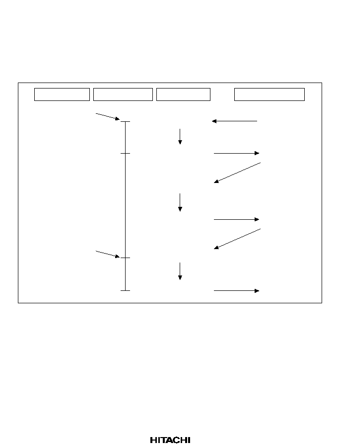
251
4. The channel 0 transfer begins.
5. When the channel 0 transfer ends, channel 0 becomes the lower-priority channel.
6. A channel 0 transfer is requested.
7. The channel 0 transfer begins.
8. When the channel 0 transfer ends, channel 0 is already the lower-priority channel, so the order
remains the same.
0
None
None
1. Requests occur
in channels
0 and 1
6. Request occurs
in channel 0
2. Channel 1
transfer starts
3. Channel 1
transfer ends
5. Channel 0
transfer ends
7. Channel 0
transfer starts
4. Channel 0
transfer starts
8. Channel 0
transfer ends
Priority
changes
1
>
0
0
>
1
1
>
0
1
>
0
Transfer requests
Waiting channel
DMAC operation
Channel priority order
Priority
changes
Priority
does not change
Waiting for
transfer request
Figure 9.5 Channel Priority in Round-Robin Mode
9.3.4
DMA Transfer Types
The DMAC supports all the transfers shown in table 9.7. It can operate in single address mode or
dual address mode, as defined by how many bus cycles the DMAC takes to access the transfer
source and transfer destination. The actual transfer operation timing varies with the DMAC bus
mode used: cycle-steal mode or burst mode.
252
Table 9.7
Supported DMA Transfers
Destination
Source
External
Device with
DACK
External
Memory
Memory-Mapped
External Device
On-Chip
Peripheral
Module
External device with DACK
Not available
Single
Single
Not available
External memory
Single
Dual
Dual
Dual
Memory-mapped external device Single
Dual
Dual
Dual
On-chip peripheral module
Not available
Dual
Dual
Dual*
Single: Single address mode
Dual:
Dual address mode
Note:
Access size enabled by the register of the on-chip peripheral module that is the source or
destination (excludes DMAC, BSC, and UBC).
Address Modes:
·
Single Address Mode
In single address mode, both the transfer source and destination are external; one (selectable) is
accessed by a DACK signal while the other is accessed by address. In this mode, the DMAC
performs the DMA transfer in one bus cycle by simultaneously outputting a transfer request
acknowledge DACK signal to one external device to access it while outputting an address to
the other end of the transfer. Figure 9.6 shows an example of a transfer between external
memory and external device with DACK. The external device outputs data to the data bus
while that data is written in external memory in the same bus cycle.
DMAC
DACK
DREQ
External
memory
External device
with DACK
SH7604
External address bus
: Data flow
External data bus
Figure 9.6 Data Flow in Single Address Mode
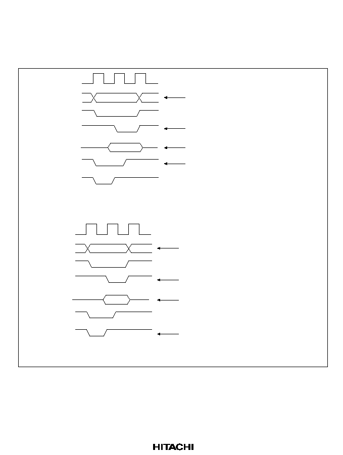
253
Two types of transfers are possible in single address mode: 1) transfers between external
devices with DACK and memory-mapped external devices; and 2) transfers between external
devices with DACK and external memory. Transfer requests for both of these must be by
means of the external request signal (DREQ). Figure 9.7 shows the DMA transfer timing for
single address mode.
CK
A26A0
CS
WE
D30D0
DACK
BS
Address output to external
memory space
Write strobe signal to external
memory space
Data output from external
device with DACK
DACK signal (active low) to external
device with DACK
a. External device with DACK to external memory space
CK
A26A0
CS
RD
D30D0
DACK
Address output to external
memory space
Data output from external
memory space
Read strobe signal to external
memory space
DACK signal (active low) to external
device with DACK
BS
b. External memory space to external device with DACK
Figure 9.7 DMA Transfer Timing in Single Address Mode
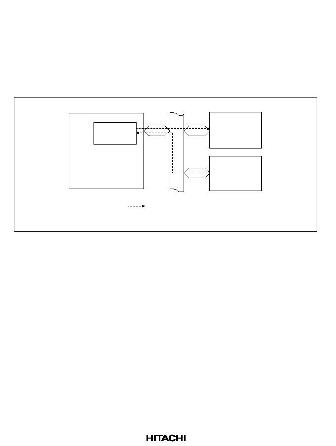
254
·
Dual Address Mode
In dual address mode, both the transfer source and destination are accessed (selectable) by
address. The source and destination can be located externally or internally. The DMAC
accesses the source in the read cycle and the destination in the write cycle, so the transfer is
performed in two separate bus cycles. The transfer data is temporarily stored in the DMAC.
Figure 9.8 shows an example of a transfer between two external memories in which data is
read from one memory in the read cycle and written to the other memory in the following write
cycle.
DMAC
External
memory
External
memory
SH7604
2
1
External data bus
: Data flow
1: Read cycle
2: Write cycle
Figure 9.8 Data Flow in Dual Address Mode
In dual address mode transfers, external memory, memory-mapped external devices and on-
chip peripheral modules can be mixed without restriction. Specifically, this enables transfers
between the following:
1. External memory and external memory.
2. External memory and memory-mapped external devices.
3. Memory-mapped external devices and memory-mapped external devices.
4. External memory and on-chip peripheral modules (excluding the DMAC, BSC, and UBC).
5. Memory-mapped external devices and on-chip peripheral modules (excluding the DMAC,
BSC, and UBC). The access size is that is enabled by the register of the on-chip peripheral
module that is the source or destination (excludes the DMAC, BSC, and UBC).
6. On-chip peripheral modules (excluding the DMAC, BSC, and UBC) and on-chip
peripheral modules (excluding the DMAC, BSC, and UBC).
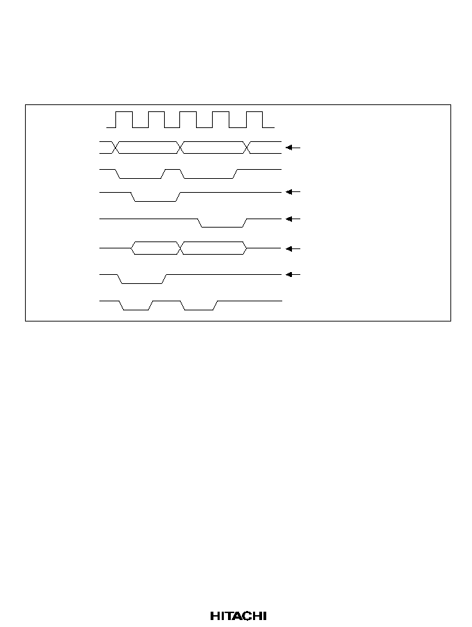
255
Transfer requests can be auto-requests, external requests, or on-chip peripheral module
requests. When the transfer request source is the SCI, however, either the data destination or
source must be the SCI (see table 9.6). Dual address mode outputs DACK in either the read
cycle or write cycle. CHCR controls the cycle in which DACK is output.
Figure 9.9 shows the DMA transfer timing in dual address mode.
CK
A26A0
D31D0
CS
RD
DACK
BS
WE
Address output to
external memory space
Read strobe signal to
external memory space
Write strobe signal to
external memory space
I/O data of external
memory space
DMAC acknowledge signal
(active-low)
Figure 9.9 DMA Transfer Timing in Dual Address Mode
(External Memory Space
External Memory Space, DACK Output in Read Cycle)
Bus Modes: There are two bus modes: cycle-steal and burst. Select the mode with the TB bits in
CHCR0 and CHCR1.
·
Cycle-Steal Mode
In cycle-steal mode, the bus right is given to another bus master after the DMAC transfers one
transfer unit (byte, word, longword, or 16 bytes). When another transfer request occurs, the bus
right is retrieved from the other bus master and another transfer is performed for one transfer
unit. When that transfer ends, the bus right is passed to the other bus master. This is repeated
until the transfer end conditions are satisfied.
Cycle-steal mode can be used with all categories of transfer destination, transfer source, and
transfer request source. The CPU may take the bus twice when an acknowledge signal is
output during the write cycle or in single address mode. Figure 9.10 shows an example of
DMA transfer timing in cycle-steal mode (dual address mode, DREQ level detection).
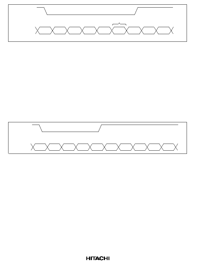
256
CPU
CPU
CPU
DMAC DMAC
CPU
DMAC
DMAC
CPU
DREQ
Bus
cycle
Bus right returned to CPU
Read
Write
Read
Write
Figure 9.10 DMA Transfer Timing in Cycle-Steal Mode
(Dual Address Mode, DREQ Level Detection)
·
Burst Mode
In burst mode, once the DMAC gets the bus, the transfer continues until the transfer end
condition is satisfied. When external request mode is used with level detection of the DREQ
pin, however, negating DREQ will pass the bus to the other bus master after completion of the
bus cycle of the DMAC that currently has an acknowledged request, even if the transfer end
conditions have not been satisfied. Burst mode cannot be used when the transfer request
originates from the serial communication interface (SCI).
Figure 9.11 shows an example of DMA transfer timing in burst mode (single address mode,
DREQ level detection).
CPU
CPU
CPU
DMAC DMAC DMAC DMAC DMAC
DREQ
Bus
cycle
DMAC
CPU
Figure 9.11 DMA Transfer Timing in Burst Mode (Single Address Mode, DREQ Level
Detection)
Refreshes cannot be performed during a burst transfer, so ensure that the number of transfers
satisfies the refresh request period when a memory requiring refreshing is used.
Relationship of Request Modes and Bus Modes by DMA Transfer Category: Table 9.8 shows
the relationship between request modes, bus modes, etc., by DMA transfer category.

257
Table 9.8
Relationship of Request Modes and Bus Modes by DMA Transfer Category
Address
Mode
Transfer Category
Request
Mode
Bus
Mode
Transfer
Size
(Bytes)
Single
External device with DACK and external memory
External
B/C
1/2/4
External device with DACK and memory-mapped
external device
External
B/C
1/2/4
Dual
External memory and external memory
All
*1
B/C
1/2/4/16
External memory and memory-mapped external
device
All
*1
B/C
1/2/4/16
Memory-mapped external device and memory-
mapped external device
All
*1
B/C
1/2/4/16
External memory and on-chip peripheral module
All
*2
B/C
*3
1/2/4/16
*4
Memory-mapped external device and on-chip
peripheral module
All
*2
B/C
*3
1/2/4/16
*4
On-chip peripheral module and on-chip peripheral
module
All
*2
B/C
*3
1/2/4/16
*4
B: Burst, C: Cycle-steal
Notes: 1. External requests and auto-requests are both available. The SCI cannot be specified as
the transfer request source, however, except for on-chip peripheral module requests.
2. External requests, auto-requests and on-chip peripheral module requests are all
available. When the SCI is the transfer request source, however, the transfer
destination or transfer source must be the SCI.
3. If the transfer request source is the SCI, cycle-steal (C) only (DREQ by edge detection,
active low).
4. The access size is that permitted by the register of the on-chip peripheral module that is
the transfer destination or source.
Bus Mode and Channel Priority: When a given channel (1) is transferring in burst mode and
there is a transfer request to a channel (0) with a higher priority, the transfer of the channel with
higher priority (0) will begin immediately. When channel 0 is also operating in the burst mode, the
channel 1 transfer will continue as soon as the channel 0 transfer has completely finished. When
channel 0 is in cycle-steal mode, channel 1 will begin operating again after channel 0 completes
the transfer of one transfer unit, but the bus will then switch between the two in the order channel
1, channel 0, channel 1, channel 0. Since channel 1 is in burst mode, it will not give the bus to the
CPU. This example is illustrated in Figure 9.12.
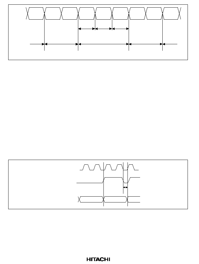
258
CPU
Bus
state
DMAC
ch1
DMAC
ch1
DMAC
ch0
DMAC
ch1
DMAC
ch0
DMAC
ch1
DMAC
ch1
CPU
ch0
ch1
ch0
DMAC ch1 and ch0
Cycle-steal
DMAC ch1
Burst mode
CPU
CPU
DMAC ch1
Burst mode
Note: Priority is ch0 > ch1, ch1 is in burst mode, ch0 is in cycle-steal mode
Figure 9.12 Bus Status when Multiple Channels are Operating
9.3.5
Number of Bus Cycles
The number of states in the bus cycle when the DMAC is the bus master is controlled by the bus
control register (BCR1) and wait state control register (WCR) of the bus state controller just as it
is when the CPU is the bus master.
9.3.6
DMA Transfer Request Acknowledge Signal Output Timing
DMA transfer request acknowledge signal DACKn is output synchronous to the DMAC address
output specified by the channel control register AM bit of the address bus. The timing is normally
to have the acknowledge signal become valid when the DMA address output begins and become
invalid 0.5 cycles before the address output ends. (See figure 9.11.) The output timing of the
acknowledge signal varies with the settings of the connected memory space. The output timing of
acknowledge signals in the memory spaces is shown in figure 9.13.
Clock
DACK
Address bus
CPU
DMAC
0.5 cycles
Figure 9.13
Example of DACK Output Timing
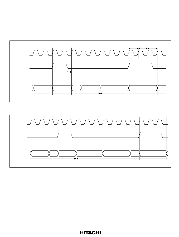
259
Acknowledge Signal Output when External Memory Is Set as Ordinary Memory Space: The
timing at which the acknowledge signal is output is the same in the DMA read and write cycles
specified by the AM bit (figures 9.14 and 9.15). When DMA address output begins, the
acknowledge signal becomes valid; 0.5 cycles before address output ends, it becomes invalid. If a
wait is inserted in this period and address output is extended, the acknowledge signal is also
extended.
Clock
DACK
Address
bus
CPU
DMAC
read
DMAC
write
Invalid
write
CPU
0.5 cycles
DMAC read
T
1
T
W
T
2
Basic timing
1 wait inserted
Figure 9.14 DACK Output in Ordinary Space Accesses (AM = 0)
Clock
DACK
Address
bus
DMAC
read
DMAC
write
Invalid
write
Invalid
write
CPU
DMAC read
Basic timing
1 wait inserted
DMAC write
Figure 9.15 DACK Output in Ordinary Space Accesses (AM = 1)
In a longword access of a 16-bit external device (figure 9.16) or an 8-bit external device (figure
9.17), or a word access of an 8-bit external device (figure 9.18), the lower and upper addresses are
output 2 and 4 times in each DMAC access in order to align the data. For all of these addresses,
the acknowledge signal becomes valid simultaneous with the start of output and becomes invalid
0.5 cycles before the address output ends. When multiple addresses are output in a single access to
align data for synchronous DRAM, DRAM, pseudo-SRAM, or burst ROM, an acknowledge
signal is output to those addresses as well.
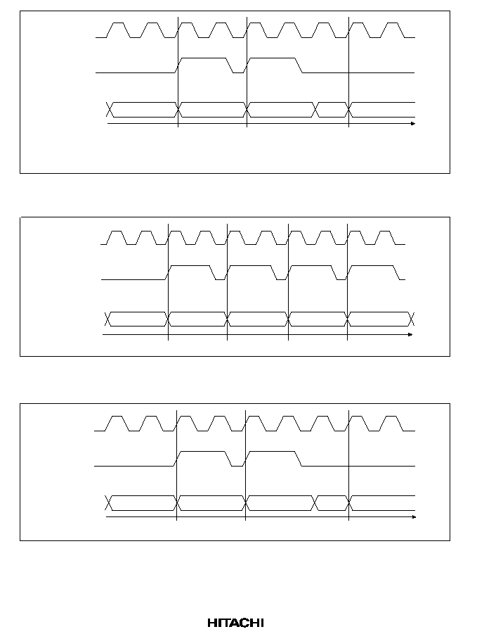
260
Clock
DACK
Address
bus
CPU H
DMAC read H
DMAC read L
Invalid
write
DMAC write
Basic timing
*1
*2
Notes: 1.
L: LSB side
2.
H: MSB side
Figure 9.16 DACK Output in Ordinary Space Accesses
(AM = 0, Longword Access to 16-Bit External Device)
Clock
DACK
Address
bus
CPU H
DMAC
read HH
DMAC
read HL
DMAC
read LH
DMAC
read LL
Basic timing
Figure 9.17 DACK Output in Ordinary Space Accesses
(AM = 0, Longword Access to 8-Bit External Device)
Clock
DACK
Address
bus
CPU H
DMAC read H
DMAC read L
Invalid
write
DMAC write
Basic timing
Figure 9.18 DACK Output in Ordinary Space Accesses
(AM = 0, Word Access to 8-Bit External Device)
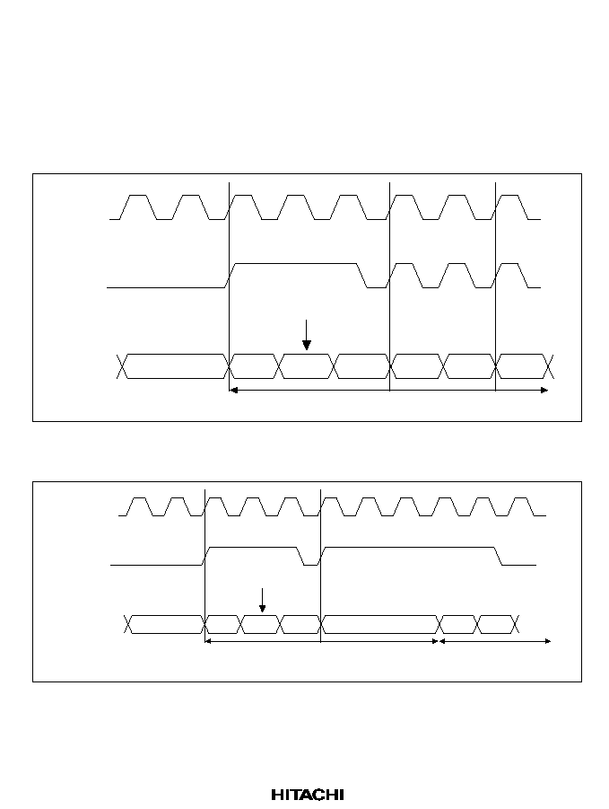
261
Acknowledge Signal Output when External Memory Is Set as Synchronous DRAM: When
external memory is set as synchronous DRAM auto-precharge and AM = 0, the acknowledge
signal is output across the row address, read command, wait and read address of the DMAC read
(figure 9.19). Since the synchronous DRAM read has only burst mode, during a single read an
invalid address is output; the acknowledge signal, however, is output on the same timing (figure
9.20). At this time, the acknowledge signal is extended until the write address is output after the
invalid read. When AM = 1, the acknowledge signal is output across the row address and column
address of the DMAC write (figure 9.21).
Clock
DACK
Address
bus
CPU
DMAC read (basic timing)
Row
address
Read 1
Read 2
Read 3
Read 4
Read
command
Figure 9.19 DACK Output in Synchronous DRAM Burst Read
(Auto-Precharge, AM = 0)
Clock
DACK
Address
bus
CPU
Invalid read
DMAC read
(basic timing)
DMAC write
(basic timing)
Row
address
Column
address
Row
address
Read
Read
command
Figure 9.20 DACK Output in Synchronous DRAM Single Read
(Auto-Precharge, AM = 0)
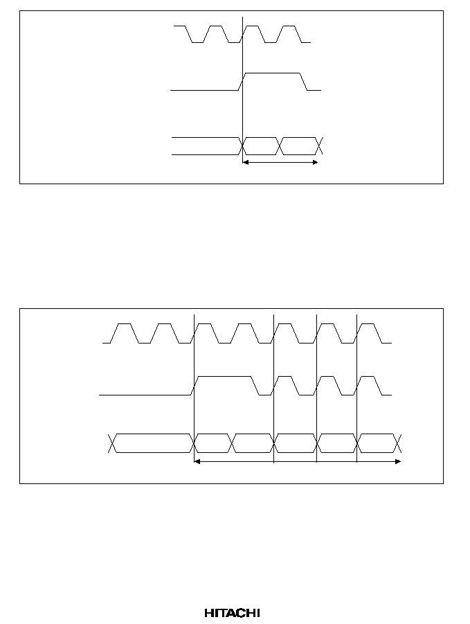
262
Clock
DACK
Address
bus
DMAC write (basic timing)
Column
address
Row
address
Figure 9.21 DACK Output in Synchronous DRAM Write
(Auto-Precharge, AM = 1)
When external memory is set as bank active synchronous DRAM, during a burst read the
acknowledge signal is output across the read command, wait and read address when the row
address is the same as the previous address output (figure 9.22). When the row address is different
from the previous address, the acknowledge signal is output across the precharge, row address,
read command, wait and read address (figure 9.23).
Clock
DACK
Address
bus
CPU
DMAC read (basic timing)
Read
command
Read 1
Read 2
Read 3
Read 4
Figure 9.22 DACK Output in Synchronous DRAM Burst Read
(Bank Active, Same Row Address, AM = 0)
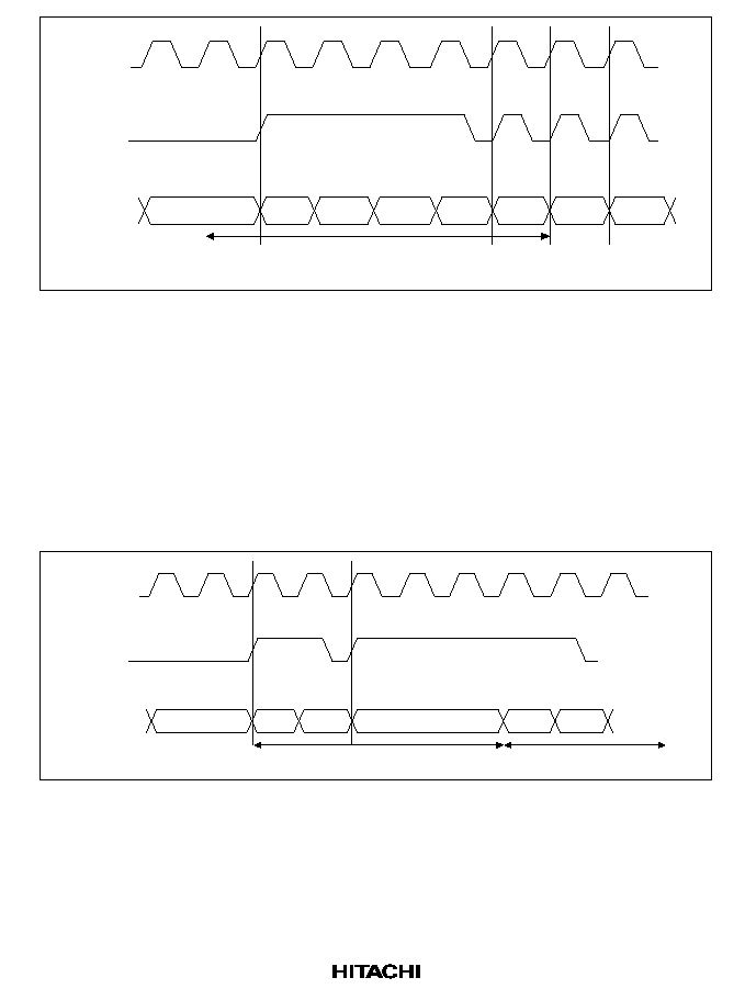
263
Clock
DACK
Address
bus
CPU
DMAC read
(basic timing)
Pre-
charge
Read
command
Read 1 Read 2 Read 3 Read 4
Row
address
Figure 9.23 DACK Output in Synchronous DRAM Burst Read
(Bank Active, Different Row Address, AM = 0)
When external memory is set as bank active synchronous DRAM, during a single read the
acknowledge signal is output across the read command, wait and read address when the row
address is the same as the previous address output (figure 9.24). When the row address is different
from the previous address, the acknowledge signal is output across the precharge, row address,
read command, wait and read address (figure 9.25). Since the synchronous DRAM read has only
burst mode, during a single read an invalid address is output; the acknowledge signal is output on
the same timing. At this time, the acknowledge signal is extended until the write address is output
after the invalid read.
Clock
DACK
Address
bus
CPU
Read
Invalid read
DMAC read (basic timing)
DMAC write (basic timing)
Read
command
Row
address
Column
address
Figure 9.24 DACK Output in Synchronous DRAM Single Read
(Bank Active, Same Row Address, AM = 0)
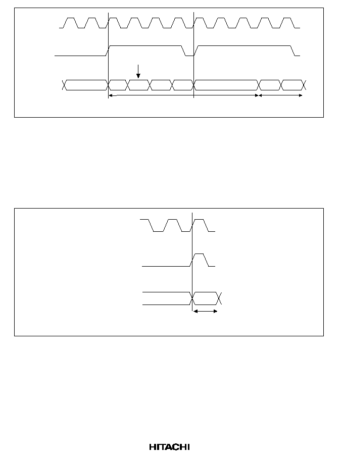
264
Clock
DACK
Address
bus
CPU
Invalid read
DMAC read
(basic timing)
DMAC write
(basic timing)
Row
address
Read
command
Row
address
Column
address
Pre-
charge
Read
Figure 9.25 DACK Output in Synchronous DRAM Single Read
(Bank Active, Different Row Address, AM = 0)
When external memory is set as bank active synchronous DRAM, during a write the acknowledge
signal is output across the wait and column address when the row address is the same as the
previous address output (figure 9.26). When the row address is different from the previous
address, the acknowledge signal is output across the precharge, row address, wait and column
address (figure 9.27).
Clock
DACK
Address
bus
DMAC write
(basic timing)
Column
address
Figure 9.26 DACK Output in Synchronous DRAM Write
(Bank Active, Same Row Address, AM = 1)
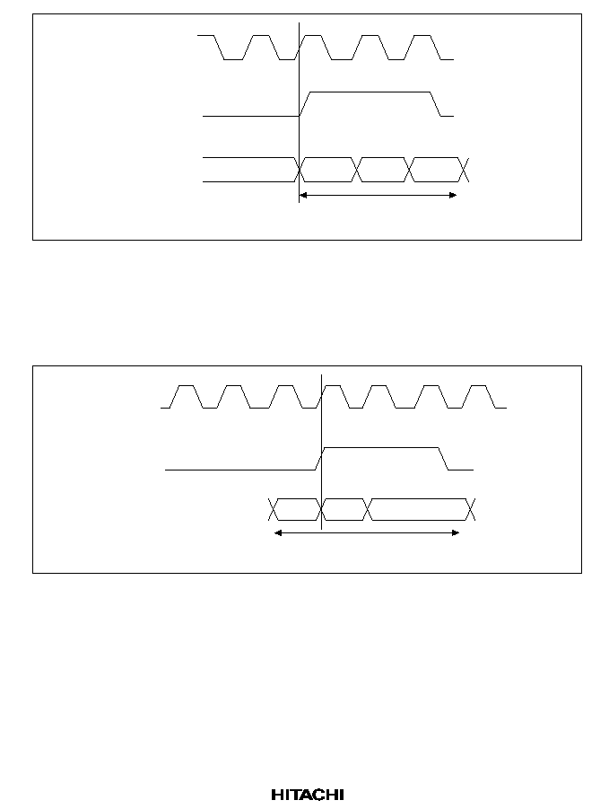
265
Clock
DACK
Address
bus
DMAC write
(basic timing)
Precharge
Row
address
Column
address
Figure 9.27 DACK Output in Synchronous DRAM Write
(Bank Active, Different Row Address, AM = 1)
Acknowledge Signal Output when External Memory Is Set as DRAM: When external memory
is set as DRAM and a row address is output during a read or write, the acknowledge signal is
output across the row address and column address (figures 9.289.30).
Clock
DACK
Address
bus
DMAC read or write
(basic timing)
Precharge
Row
address
Column address
Figure 9.28 DACK Output in Normal DRAM Accesses (AM = 1 or 0)
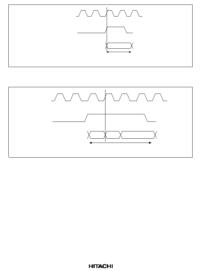
266
Clock
DACK
Address
bus
DMAC read or write
(basic timing)
Column
address
Figure 9.29 DACK Output in DRAM Burst Accesses
(Same Row Address, AM = 1 or 0)
Clock
DACK
Address
bus
DMAC read or write
(basic timing)
Pre-
charge
Row
address
Column address
Figure 9.30 DACK Output in DRAM Burst Accesses
(Different Row Address, AM = 1 or 0)
Acknowledge Signal Output when External Memory Is Set as Pseudo-SRAM: When external
memory is set as pseudo-SRAM , the acknowledge signal is output synchronous to the DMAC
address for both reads and writes (figures 9.319.33).
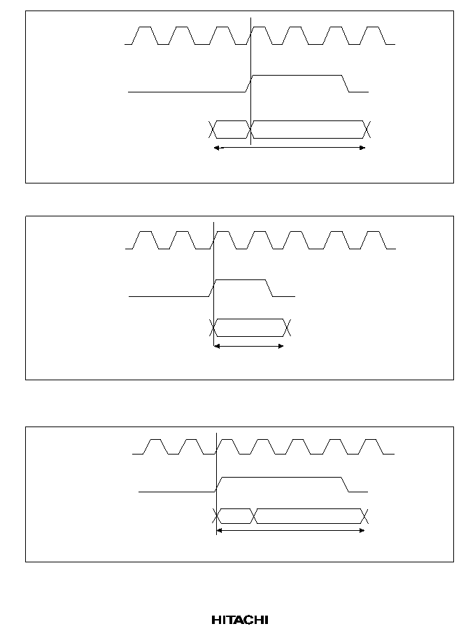
267
Clock
DACK
Address
bus
DMAC read or write
(basic timing)
Pre-
charge
DMAC address
Figure 9.31 DACK Output in Normal Pseudo-SRAM Accesses (AM = 1 or 0)
Clock
DACK
Address
bus
DMAC read or write
(basic timing)
DMAC address
Figure 9.32 DACK Output in Pseudo-SRAM Burst Accesses
(Same Row Address, AM = 1 or 0)
Clock
DACK
Address
bus
DMAC read or write
(basic timing)
DMAC address
Pre-
charge
Figure 9.33 DACK Output in Pseudo-SRAM Burst Accesses
(Different Row Address, AM = 1 or 0)
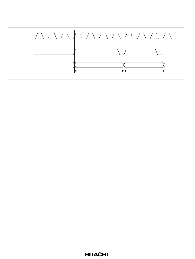
268
Acknowledge Signal Output When External Memory Is Set as Burst ROM: When external
memory is set as burst ROM, the acknowledge signal is output synchronous to the DMAC address
(no dual writes allowed) (figure 9.34).
Clock
DACK
Address
bus
DMAC (1 wait state)
DMAC cycle
DMAC cycle
Figure 9.34 DACK Output in Nibble Accesses of Burst ROM
9.3.7
DREQ Pin Input Detection Timing
In external request mode, DREQ pin signals are usually detected at the rising edge of the clock
pulse (CKIO). When a request is detected, a DMAC bus cycle is produced three cycles later at the
earliest and a DMA transfer performed. After the request is detected, the timing of the next input
detection varies with the bus mode, address mode, method of DREQ input detection, and the
memory connected.
DREQ Pin Input Detection Timing in Cycle-Steal Mode:
In cycle-steal mode, once a request is detected from the DREQ pin, request detection for the next
DMA transfer cannot be performed for a certain period of time. After request detection has again
become possible, detectable cycles continue until a request is detected.
Figure 9.35 illustrates the timing from the detection of a request till the next time requests are
detectable.
·
Cycle-Steal Mode Edge Detection
Requests can be detected 2 cycles after DACK output. After that point, the request is input to
DREQ. (If input prior to that point, a request may or may not be detected, depending on the
internal state.)
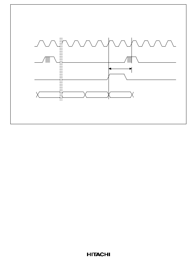
269
Transfer width: Byte, word, longword
Transfer bus mode: Cycle-steal mode
Transfer address modes: Dual and single modes
DREQ detection method: Edge detection
DACK output timing: Read, write (dual), DMAC cycle (single)
Bus cycle: Basic bus cycle
CPU
Clock
DREQ
DACK
1st acceptance
*
1
*
1
2 cycles
Bus
cycle
CPU
*
2
DMAC
2nd acceptance
Notes: 1. Request detection
2. When DACK is output in a write (dual), the cycle is a DMAC read. Otherwise, the cycle
is a CPU cycle.
Figure 9.35 DREQ Pin Input Detection Timing in Cycle-Steal Mode with Edge
Detection (1)
Figures 9.36 and 9.37 show examples of how to change the bus width of an external device.
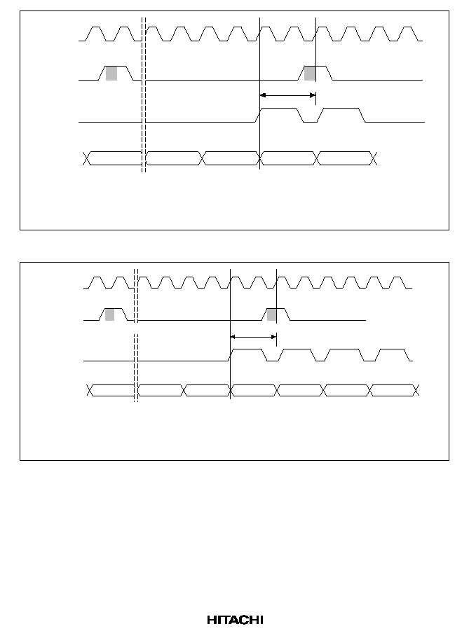
270
CPU
Clock
DREQ
DACK
*
1
*
1
Bus
cycle
CPU
*
2
DMAC H
DMAC L
1st acceptance
2 cycles
2nd acceptance
Notes: 1. Request detection
2. When DACK is output in a write (dual), the cycle is a DMAC read. Otherwise, the cycle
is a CPU cycle.
Figure 9.36 Changing the Bus Size of a 16-Bit External Device
CPU
DREQ
DACK
CPU
*
2
DMAC HH DMAC HL
DMAC LH
DMAC LL
Clock
*
1
*
1
Bus
cycle
2 cycles
2nd acceptance
1st acceptance
Notes: 1. Request detection
2. When DACK is output in a write (dual), the cycle is a DMAC read. Otherwise, the cycle
is a CPU cycle.
Figure 9.37 Changing the Bus Size of an 8-Bit External Device
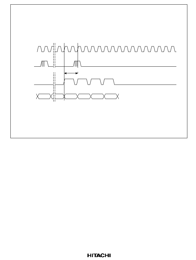
271
Transfer width: 16-byte
Transfer bus mode: Cycle-steal mode
Transfer address mode: Dual mode
DREQ detection method: Edge detection
DACK output timing: DMAC read and write cycles
Bus cycle: Basic bus cycle
CPU
*
2
DMAC 1
DMAC 2
DMAC 3
DMAC 4
DREQ
DACK
Clock
*
1
*
1
Bus
cycle
2 cycles
2nd acceptance
1st acceptance
*
3
*
3
*
3
*
3
Notes
1.
Request detection
2.
When a write (dual) occurs at DACK output, the cycle is a DMAC read.
Otherwise, the cycle is a CPU cycle.
3.
When DACK is output in a write (dual), the cycle is a DMAC write; when in a read
(dual), the cycle is a DMAC read.
Figure 9.38 DREQ Pin Input Detection Timing in Cycle-Steal Mode with Edge
Detection (2)
Requests can be detected 2 cycles after DACK output. After that point, the request is input to
DREQ. (If input prior to that point, a request may or may not be detected, depending on the
internal state.) DACK is output synchronous to all 4 transfers (figure 9.38).
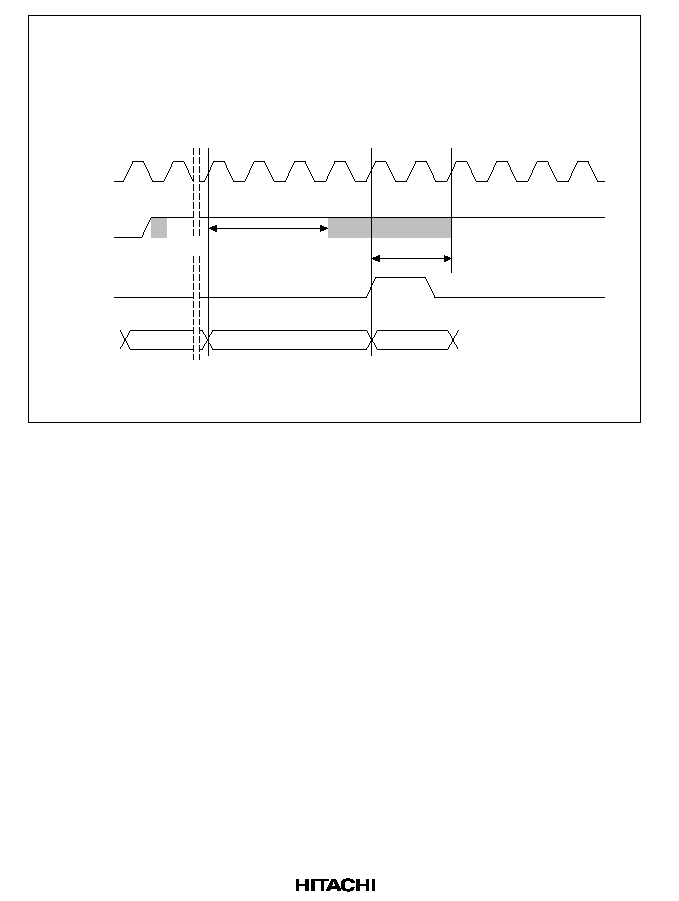
272
Transfer width: Byte, word, longword
Transfer bus mode: Cycle-steal mode
Transfer address modes: Dual and single modes
DREQ detection method: Level detection
DACK output timing: Read (dual), DMAC cycle (single)
Bus cycle: Basic bus cycle
CPU
DREQ
DACK
CPU
DMAC read
*
2
Clock
*
1
Bus
cycle
3 cycles
2 cycles
Area where 2nd
acceptance is possible
1st acceptance
Notes: 1. Request detection
2. Request detection not established.
Figure 9.39 Timing of DREQ Pin Input Detection in Cycle-Steal Mode
with Level Detection (1)
·
Cycle-Steal Mode Level Detection
Requests can be detected for the first time 3 cycles after the bus cycle prior to the DMAC read
cycle and detection starts sometime between then and 2 cycles after DACK output (figure 9.40,
41). This varies with variations in waits and the like. This means that if request output is
stopped within 3 cycles from the bus cycle prior to the DMAC read cycle, the next DMA
transfer is not performed; if request output is stopped within 2 cycles of DACK output, the
next DMA transfer may sometimes be performed. See Examples of Handling of Request
Signal Acceptance later in this section (9.3.7).
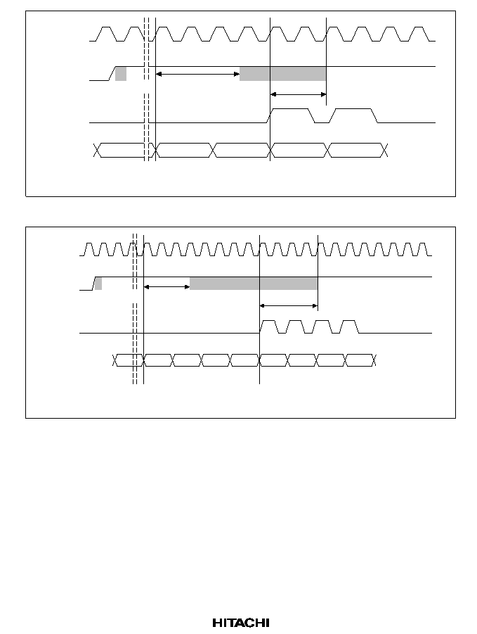
273
CPU
DREQ
DACK
CPU H
CPU L
DMAC H
DMAC L
*
2
Clock
*
1
Bus cycle
3 cycles
2 cycles
Area where 2nd
acceptance is possible
1st acceptance
Notes: 1. Request detection
2. Request detection not established.
Figure 9.40 Changing the Bus Size of a 16-Bit External Device
CPU HH
CPU HL
CPU LH
CPU LL
DMAC HH
DMAC HL
DMAC LH
DMAC LL
DREQ
DACK
*
2
Clock
*
1
Bus
cycle
3 cycles
2 cycles
Area where 2nd
acceptance is possible
1st acceptance
Notes: 1. Request detection
2. Request detection not established.
Figure 9.41 Changing the Bus Size of an 8-Bit External Device
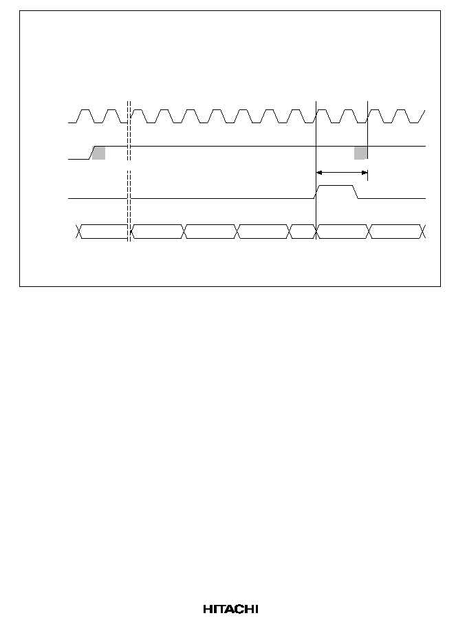
274
Transfer width: Byte, word, longword
Transfer bus mode: Cycle-steal mode
Transfer address mode: Dual mode
DREQ detection method: Level detection
DACK output timing: DMAC write cycle
Bus cycle: Basic bus cycle
DREQ
DACK
CPU
CPU
DMAC read
DMAC write
CPU
Clock
*
*
Bus
cycle
2 cycles
1st acceptance
2nd acceptance
CPU
Invalid
write
Note: Request detection
Figure 9.42 Timing of DREQ Pin Input Detection in Cycle Steal Mode
with Level Detection (2)
The next request can be detected 2 cycles after DACK output (figure 9.42).
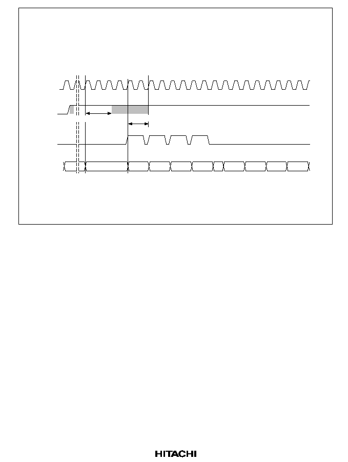
275
Transfer width: 16-byte
Transfer bus mode: Cycle-steal mode
Transfer address mode: Dual mode
DREQ detection method: Level detection
DACK output timing: DMAC write cycle
Bus cycle: Basic bus cycle
CPU
DMAC
read 1
DMAC
read 2
DMAC
read 3
DMAC
read 4
DMAC
write 1
DMAC
write 2
DMAC
write 3
DMAC
write 4
DREQ
DACK
*2
Clock
*1
Bus
cycle
3 cycles
2 cycles
2nd acceptance
1st acceptance
Invalid
write
CPU
Notes: 1. Request detection
2. Request detection not established.
Figure 9.43 Timing of DREQ Pin Input Detection in Cycle Steal Mode
with Level Detection (3)
Requests can be detected for the first time 3 cycles after the bus cycle prior to the DMAC read
cycle and starts sometime between then and 2 cycles after DACK output (figure 9.43). This varies
with variations in waits and the like. This means that if request output is stopped within 3 cycles
from the bus cycle prior to the DMAC read cycle, the next DMA transfer is not performed; if
request output is stopped within 2 cycles of DACK output, the next DMA transfer may sometimes
be performed.
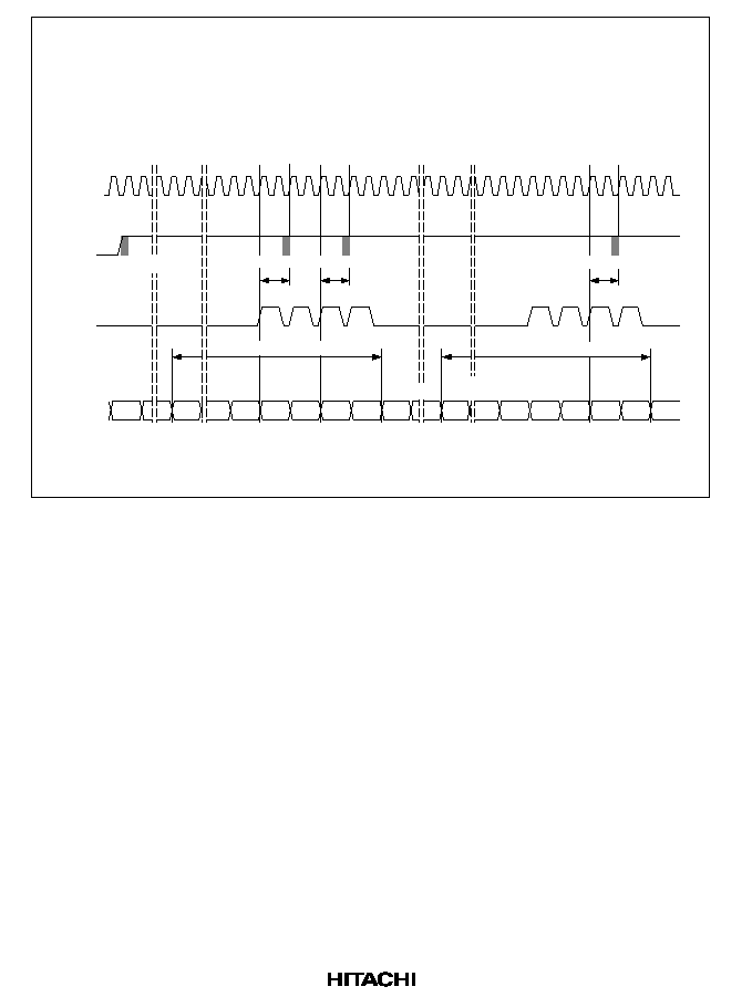
276
Transfer width: 16-byte
Transfer bus mode: Cycle-steal mode
Transfer address mode: Dual mode
DREQ detection method: Level detection
DACK output timing: DMAC write cycle
Bus cycle: Basic bus cycle
DMAC
read 4
CPU
CPU
DREQ
DACK
A1
A2
A3
A4
B1
B2
B3
B4
Clock
Bus
cycle
2 cycles
1st acceptance
*
*
*
*
2 cycles
2 cycles
4th acceptance
2nd acceptance 3rd acceptance
2nd 16-byte transfer
1st 16-byte transfer
Invalid
write
DMAC
read 1
DMAC
write 1
DMAC
write 2
DMAC
write 3
CPU
DMAC
write 4
DMAC
read 1
Invalid
write
DMAC
write 1
DMAC
write 2
DMAC
write 3
DMAC
write 4
CPU
CPU
DMAC
read 4
Note: Request detection
Figure 9.44 Timing of DREQ Pin Input Detection in Cycle Steal Mode
with Level Detection (4)
For 16-byte transfers, DACK signals are output at all consecutive writes (figure 9.44). The
acknowledge signals are A1, A2, A3, A4, B1, B2, B3, B4, ....
The second transfer request can be detected 2 cycles after output of acknowledge signal A1. The
third transfer request is detected at A3, that is, 2 cycles after output of the third acknowledge
signal of the first transfer. The fourth transfer request is detected 2 cycles after output of B3.
Requests thereafter are detected 2 cycles after the third acknowledge signal of each transfer, as
with the fourth transfer.
Note:
When transferring alternately on channels 0 and 1 by round robin or the like, the next
request signal is detected only 2 cycles after the first acknowledge signal of each transfer
(figure 9.45).
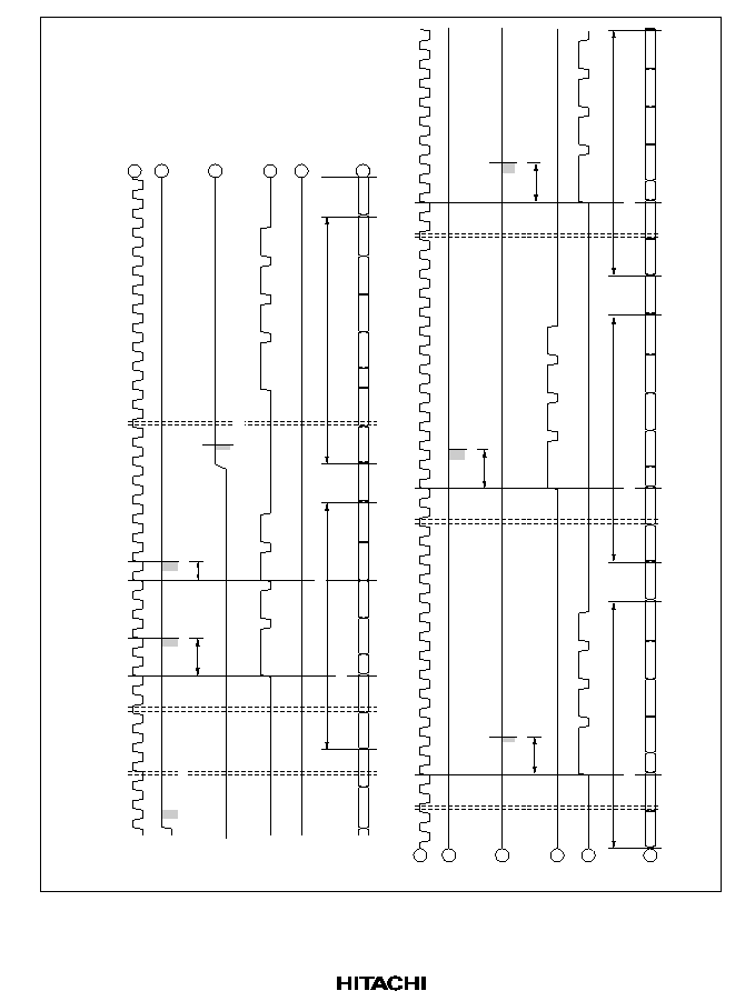
277
B4
CPU
B3
B2
B1
2 cycles
2 cycles
DMAC
read 1
A4
CPU
CPU
Bus
cycle
DACK1
DACK0
DREQ1
DREQ0
CK
DMAC
read 4
A3
A2
A1
**
B4
B3
B2
B1
2 cycles
C4
C3
C2
C1
2 cycles
A4
A3
A2
A1
2 cycles
*
*
1st acceptance
2nd acceptance
3rd acceptance
1st acceptance
1st 0 ch 16-byte transfer
2nd 0 ch 16-byte transfer
CPU
DMAC
write 1
DMAC
write 2
DMAC
write 3
DMAC
write 4
DMAC
read 1
DMAC
read 4
Invalid
write
DMAC
write 1
DMAC
write 2
DMAC
write 3
DMAC
write 4
*
*
*
3rd acceptance
4th acceptance
2nd acceptance
1st 1 ch 16-byte transfer
3rd 0 ch 16-byte transfer
2nd 1 ch 16-byte transfer
DMAC
read 1
DMAC
read 4
DMAC
write 1
Invalid
write
Invalid
write
DMAC
write 2
DMAC
write 3
DMAC
write 4
CPU
DMAC
read 1
DMAC
read 4
Invalid
write
DMAC
write 1
DMAC
write 3
CPU
DMAC
write 2
DMAC
write 4
DMAC
read 1
DMAC
read 4
Invalid
write
DMAC
write 1
DMAC
write 3
DMAC
write 2
DMAC
write 4
2
3
1
4
5
6
2
3
1
4
5
6
Transfer width: 16-byte
Transfer bus mode: Cycle-steal mode
Transfer address mode: Dual mode
Priority mode: Round robin mode
Note: Request detection timing
DREQ detection method: Level detection
DACK output timing: DMAC write cycle
Bus cycle: Basic bus cycle
Figure 9.45 Example of Simultaneous Operation of 2 Channels
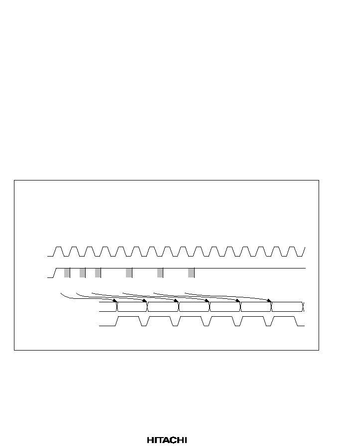
278
DREQ Pin Input Detection Timing in Burst Mode: In burst mode, the request detection timing
differs when DREQ input is detected by edge and when detected by level.
When DREQ input is detected by edge, once a request is detected, DMA transfers continue until
the conditions for ending the transfers are met, regardless of the state of the DREQ pin thereafter.
During this period, requests cannot be detected. When the transfer start conditions are met after a
transfer ends, requests can be detected again for each cycle.
When DREQ input is detected by level, whenever a request is detected for the same channel as in
the next request detection cycle, that channel is executed continuously. When no request is input,
however, the bus cycles of other channels and other bus masters are executed.
·
Burst Mode, Single Mode, Level Detection
Acknowledge signals for request signals are output 3 cycles later at the earliest. Even when the
request signal is dropped within 2 cycles of the output of this acknowledge signal, the fourth or
fifth requests in figure 9.46 are accepted. This means that 4 or 5 DMA transfers are executed
even when the request for the 1st acknowledge signal drops out.
Transfer width: Byte, word, longword
Transfer bus mode: Burst mode
Transfer address mode: Single mode
DREQ detection method: Level detection
DACK output timing: DMAC cycle
Bus cycle: Basic bus cycle
DREQ
DACK
DMAC read 1
Clock
Bus
cycle
*
1st
accept-
ance
3rd
accept-
ance
4th
accept-
ance
2nd
accept-
ance
*
*
*
*
5th
accept-
ance
6th
accept-
ance
DMAC read 2 DMAC read 3 DMAC read 4
DMAC read 5 DMAC read 6
*
Note: Request detection (The points when the acceptances occur vary with the type of wait.)
Figure 9.46 Timing of DREQ Pin Input Detection in Burst Mode with Level Detection (1)
(Data Transfer from Normal Space to Device)
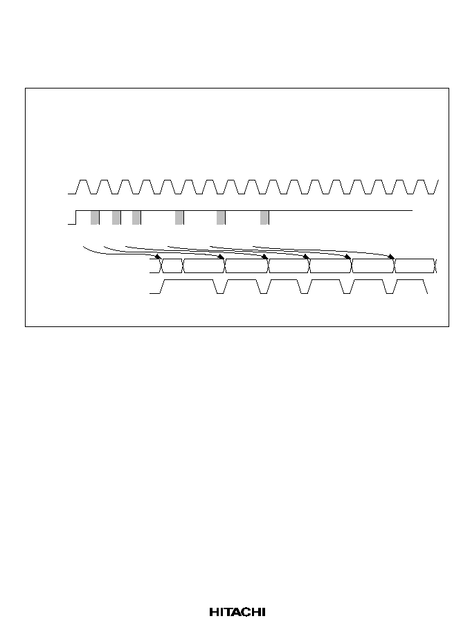
279
Acknowledge signals for request signals are output 4 cycles later, at the soonest. Even when the
request signal is dropped within 0.5 cycle of the output of this acknowledge signal, the third
request in figure 9.46 is accepted. This means that the 3rd DMA transfer is executed even when
the request for the 1st acknowledge signal drops out. The detection timing for the 4th and
subsequent requests is as shown in figure 9.46.
Transfer width: Byte, word, longword
Transfer bus mode: Burst mode
Transfer address mode: Single mode
DREQ detection method: Level detection
DACK output timing: DMAC cycle
Bus cycle: Basic bus cycle
DREQ
DACK
Clock
Bus
cycle
*
*
*
1st
accept-
ance
3rd
accept-
ance
4th
accept-
ance
2nd
accept-
ance
5th
accept-
ance
6th
accept-
ance
DMAC write 1 DMAC write 2 DMAC write 3 DMAC write 4 DMAC write 5 DMAC write 6
Invalid
write
*
*
*
Note: Request detection (The points when the acceptances occur vary with the type of wait.)
Figure 9.47 Timing of DREQ Pin Input Detection in Burst Mode with Level Detection (2)
(Data Transfer from Device to Normal Space)
Acknowledge signals for request signals are output 4 cycles later at the earliest. Even when the
request signal is dropped within 0.5 cycle of the output of this acknowledge signal, the third
request in figure 9.47 is accepted. This means that the 3rd DMA transfer is executed even when
the request for the first acknowledge signal drops out. The detection timing for the 4th and
subsequent requests is a shown in figure 9.47.
Note on Evaluation Chip: The request signal detection timing in the evaluation chip differs from
that in the user chip. The evaluation chip detection timing corresponding to figures 9.46 and 9.47
is shown in figures 9.48 and 9.49.
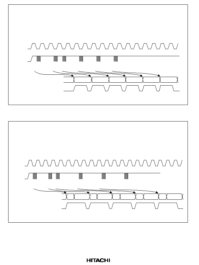
280
Transfer width: Byte, word, longword
Transfer bus mode: Burst mode
Transfer address mode: Single mode
DREQ detection method: Level detection
DACK output timing: DMAC cycle
Bus cycle: Basic bus cycle
*
Clock
Bus
cycle
DREQ
DACK
1st
accept-
ance
3rd
accept-
ance
4th
accept-
ance
2nd
accept-
ance
5th
accept-
ance
6th
accept-
ance
DMAC read 1 DMAC read 2 DMAC read 3 DMAC read 4 DMAC read 5 DMAC read 6
*
*
*
*
*
Note: Request detection (The points when the acceptances occur vary with the type of wait.)
Figure 9.48 Timing of DREQ Pin Input Detection in Burst Mode with Level Detection (3)
(Data Transfer from Normal Space to Device, Using Evaluation Chip)
Transfer width: Byte, word, longword
Transfer bus mode: Burst mode
Transfer address mode: Single mode
DREQ detection method: Level detection
DACK output timing: DMAC cycle
Bus cycle: Basic bus cycle
Clock
DREQ
Bus
cycle
DACK
*
*
*
*
*
*
1st
accept-
ance
2nd
accept-
ance
3rd
accept-
ance
4th
accept-
ance
5th
accept-
ance
6th
accept-
ance
Invalid
write
Invalid
write
DMAC
write 1
DMAC
write 2
DMAC
write 3
DMAC
write 4
DMAC
write 5
Invalid
write
Invalid
write
Invalid
write
Note: Request detection (The points when the acceptances occur vary with the type of wait.)
Figure 9.49 Timing of DREQ Pin Input Detection in Burst Mode with Level Detection (4)
(Data Transfer from Device to Normal Memory, Using Evaluation Chip)
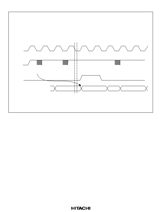
281
·
Burst Mode, Dual Mode, Level Detection
Transfer width: Byte, word, longword
Transfer bus mode: Burst mode
Transfer address mode: Single mode
DREQ detection method: Level detection
DACK output timing: DMAC read
Bus cycle: Basic bus cycle
CPU
DMAC read
DMAC read
DMAC
invalid write
Clock
DREQ
DACK
1st
acceptance
*
2nd
acceptance
3rd
acceptance
*
*
Bus
cycle
Note: Request detection (The points when the 1st and 2nd acceptances occur vary with the
type of wait.)
Figure 9.50 Timing of DREQ Pin Input Detection in Burst Mode with Level Detection (5)
Acknowledge signals for request signals are output 4 cycles later, at the soonest. Even when
the request signal is dropped within 0.5 cycle of the output of the acknowledge signal, the 2nd
request in figure 9.50 is accepted. This means that two DMA transfers are executed even when
the request for the 1st acknowledge signal drops out.
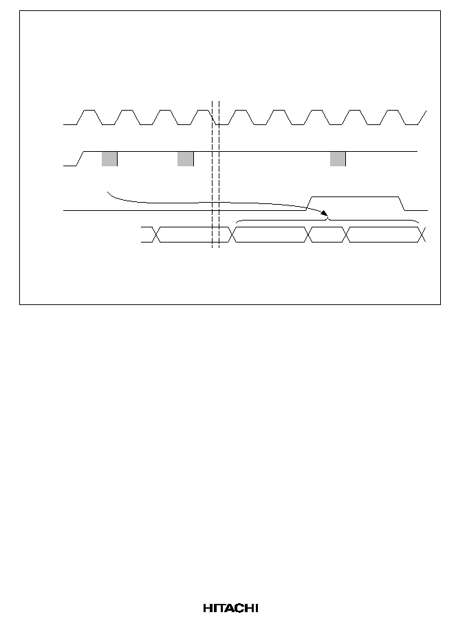
282
Transfer width: Byte, word, longword
Transfer bus mode: Burst mode
Transfer address mode: Dual mode
DREQ detection method: Level detection
DACK output timing: DMAC write
Bus cycle: Basic bus cycle
CPU
DMAC read
DMAC write
DMAC
invalid write
Clock
DREQ
DACK
Bus
cycle
1st
acceptance
*
2nd
acceptance
3rd
acceptance
*
*
Note: Request detection (The points when the 1st and 2nd acceptances occur vary with the
type of wait.)
Figure 9.51 Timing of DREQ Pin Input Detection in Burst Mode with Level Detection (6)
Acknowledge signals for request signals are output 6 cycles later, at the soonest. Even when
the request signal is dropped within 0.5 cycle of the output of the acknowledge signal, the 2nd
request in figure 9.51 is accepted. This means that two DMA transfers are executed even when
the request for the 1st acknowledge signal drops out.
Examples of Handling of Request Signal Acceptance: When DREQ level acceptance is used in
the cycle-steal mode, the following methods can be used when the request signal is received:
1. Control the number of transfers by TCR
2. Use edge for request acceptance
3. Perform acknowledge signal output at the DMAC write timing
Additional Cautions when Emulators Are Used: When DREQ level acceptance is by an
emulator in cycle-steal mode, the timing of request signal acceptance is 2 cycles after the output of
the acknowledge signal, so it differs from ordinary specifications. This means that when DMAC
operation is emulated, the timing is somewhat different, which may have other ramifications.
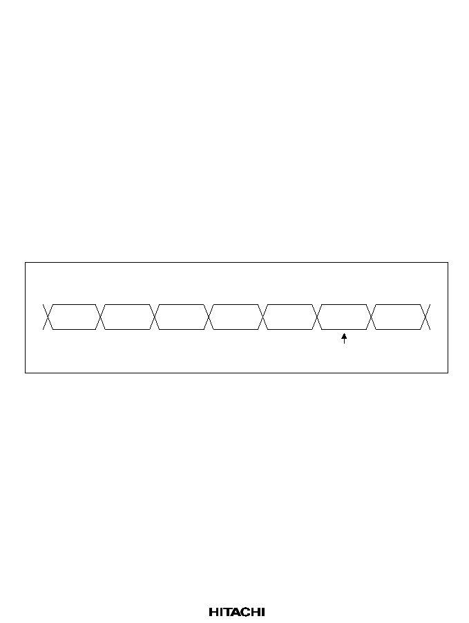
283
9.3.8
DMA Transfer End
The DMA transfer ending conditions vary when channels end individually and when both
channels end together.
Conditions for Channels Ending Individually: When either of the following conditions are met,
the transfer will end in the relevant channel only:
·
The value of the channel's DMA transfer count register (TCR) becomes 0.
When the TCR value becomes 0, the DMA transfer for that channel ends and the transfer-end
flag bit (TE) is set in CHCR. If the IE (interrupt enable) bit has already been set, a DMAC
interrupt (DEI) request is sent to the CPU. In 16-byte transfer, when the TCR is 3,2,1 during
the final transfer, the source address will be output four times, but the destination address will
only be output the number of times found in TCR before transfer ends.
·
The DE bit of the DMA channel control register (CHCR) is cleared to 0.
When the DMA enable bit (DE) in CHCR is cleared, DMA transfers in the affected channel
are halted. The TE bit is not set when this happens.
Source
address
first time
Source
address
second time
Source
address
third time
Source
address
fourth time
Destination
address
first time
Destination
address
second time
CPU
TCR = 0
(transfer ends normally)
Figure 9.52 16-Byte Transfer when TCR = 2
Conditions for Both Channels Ending Simultaneously: Transfers on both channels end when
either of the following conditions is met:
·
The NMIF (NMI flag) bit or AE (address error flag) bit is set to 1 in DMAOR.
When an NMI interrupt or DMAC address error occurs and the NMIF or AE bit is set to 1 in
DMAOR, all channels stop their transfers. The DMA source address register (SAR),
designation address register (DAR), and transfer count register (TCR) are all updated by the
transfer immediately preceding the halt. When this transfer is the final transfer, TE = 1 and the
transfer ends. To resume transfer after NMI interrupt exception handling or address error
exception handling, clear the appropriate flag bit. When the DE bit is then set to 1, the transfer
on that channel will restart. To avoid this, keep its DE bit at 0. In dual address mode, DMA
transfer will be halted after the completion of the following write cycle even when the address
error occurs in the initial read cycle. SAR, DAR and TCR are updated by the final transfer.

284
·
The DMA master enable (DME) bit in DMAOR is cleared to 0.
Clearing the DME bit in DMAOR forcibly aborts the transfers on both channels at the end of
the current bus cycle. When the transfer is the final transfer, TE = 1 and the transfer ends.
9.4
Examples of Use
9.4.1
DMA Transfer Between On-Chip SCI and External Memory
In the following example, data received on the on-chip serial communication interface (SCI) is
transferred to external memory using DMAC channel 1. Table 9.9 shows the transfer conditions
and register settings.
Table 9.9
Register Settings for Transfers between On-Chip SCI and External Memory
Transfer Conditions
Register
Setting
Transfer source: RDR of on-chip SCI
SAR1
H'FFFFFE05
Transfer destination: external memory (word space)
DAR1
Destination address
Number of transfers: 64
TCR1
H'0040
Transfer destination address: incremented
CHCR1
H'4045
Transfer source address: fixed
Bus mode: cycle-steal
Transfer unit: byte
DEI interrupt request generated at end of transfer (DE = 1)
Channel priority: Fixed (0 > 1) (DME = 1)
DMAOR
H'0001
Transfer request source (transfer request signal): SCI (RXI)
DRCR1
H'01
Note:
Check the CPU interrupt level when interrupts are enabled in the SCI.

285
9.5
Usage Notes
1. DMA request/response selection control registers 0 and 1 (DRCR0 and DRCR1) should be
accessed in bytes. All other registers should be accessed in longword units.
2. Before rewriting CHCR0, CHCR1, DRCR0, and DRCR1, first clear the DE bit for the
specified channel to 0 or clear the DME bit in DMAOR to 0.
3. When the DMAC is not operating, the NMIF bit in DMAOR is set even when an NMI
interrupt is input.
4. When the cache is used as on-chip RAM, the DMAC cannot access this RAM.
5. Set to standby mode after the DME bit in DMAOR is set to 0.
6. Do not access the DMAC, BSC, and UBC on-chip peripheral modules.
7. Do not access the cache (address array, data array, associative purge area).
8. To detect the DREQ pin signal in single address mode, use edge detection.

286

287
Section 10 Division Unit
10.1
Overview
The division unit (DIVU) divides 64 bits by 32 bits and 32 bits by 32 bits. The results are
expressed as a 32-bit quotient and a 32-bit remainder. When the operation produces an overflow,
an interrupt can be generated as specified.
10.1.1
Features
The division unit has the following features:
·
Performs signed division of 64 bits by 32 bits and 32 bits by 32 bits
·
Handles 32-bit quotient, 32-bit remainder
·
Completes operation execution in 39 cycles
·
Controls enabling/disabling of over/underflow interrupts
·
Even during the division process, instructions not accessing the division unit can be parallel-
processed
288
10.1.2
Block Diagram
Figure 10.1 shows a block diagram of the division unit.
VCRDIV
DVCR
DVDNTL
DVDNTH
DVDNT
Division
control
circuit
Bus
interface
Division
oper-
ation
circuit
Module data bus
Internal data bus
Internal interrupt signal
DVSR
DVSR: Divisor register
DVDNT: Dividend register L for 32-bit division
DVDNTH: Dividend register H
DVDNTL: Dividend register L
DVCR: Division control register
VCRDIV: Vector number setting register DIV
Figure 10.1 Division Unit Block Diagram
10.1.3
Register Configuration
Table 10.1 shows the register configuration of the division unit.
289
Table 10.1
Division Unit Register Configuration
Register
Abbr.
R/W
Initial Value Address
Access Size
*1
Divisor register
DVSR
R/W
Undefined
H'FFFFFF00
32
Dividend register L for 32-bit
division
DVDNT
R/W
Undefined
H'FFFFFF04
32
Division control register
DVCR
R/W
H'00000000
H'FFFFFF08
16, 32
Vector number setting register
DIV
VCRDIV
R/W
Undefined
*2
H'FFFFFF0C
16, 32
Dividend register H
DVDNTH R/W
Undefined
H'FFFFFF10
32
Dividend register L
DVDNTL
R/W
Undefined
H'FFFFFF14
32
Notes: 1. Accesses to the division unit are read and written in 32-bit units. DVCR and VCRDIV
permit 16 and 32-bit accesses. When registers other than CONT and VCRDIV are
accessed with word accesses, undefined values are read or written.
2. The initial value of VCRDIV is H'0000**** (asterisks represent undefined values).
10.2
Description of Registers
10.2.1
Divisor Register (DVSR)
Bit:
31
30
29
...
3
2
1
0
Bit name:
...
Initial value:
--
--
--
...
--
--
--
--
R/W:
R/W
R/W
R/W
...
R/W
R/W
R/W
R/W
The divisor register (DVSR) is a 32-bit read/write register in which the divisor for the operation is
written. It is not initialized by a power-on reset or manual reset, in standby mode, or during
module standbys.
10.2.2
Dividend Register L for 32-Bit Division (DVDNT)
Bit:
31
30
29
...
3
2
1
0
Bit name:
...
Initial value:
--
--
--
...
--
--
--
--
R/W:
R/W
R/W
R/W
...
R/W
R/W
R/W
R/W
290
The dividend register L for 32-bit division (DVDNT) is a 32-bit read/write register in which the
32-bit dividend used for 32-bit
÷
32-bit division operations is written. When 32-bit
÷
32-bit
division is run, the value set as the dividend is lost and the quotient written at the end of division.
When this register is written to, the same value is written in the DVDNTL register. The MSB
written is sign-extended in the DVDNTH register. Writing to this register starts the 32-bit
÷
32-bit
division operation. It is not initialized by a power-on reset or manual reset, in standby mode, or
during module standbys.
10.2.3
Division Control Register (DVCR)
Bit:
31
30
29
...
3
2
1
0
Bit name:
--
--
--
...
--
--
OVFIE
OVF
Initial value:
0
0
0
...
0
0
0
0
R/W:
R
R
R
...
R
R
R/W
R/W
The division control register (DVCR) is a 32-bit read/write register, but is also 16-bit accessible. It
controls enabling/disabling of the overflow interrupt. This register is initialized to H'00000000 by
a power-on reset or manual reset. It is not initialized in standby mode or during module standbys.
·
Bits 31 to 2: Reserved. These bits always read 0. The write value should always be 0.
·
Bit 1: OVF Interrupt Enable (OVFIE): Selects enabling or disabling of the OVF interrupt
request (OVFI) upon overflow.
Bit 1: OVFIE
Description
0
Interrupt request (OVFI) caused by OVF disabled
(Initial value)
1
Interrupt request (OVFI) caused by OVF enabled
Note:
Always set the OVFIE bit before starting the operation whenever executing interrupt
handling for overflows.
·
Bit 0: Overflow Flag (OVF). Flag indicating an overflow has occurred.
Bit 0: OVF
Description
0
No overflow has occurred
(Initial value)
1
Overflow has occurred

291
10.2.4
Vector Number Setting Register DIV (VCRDIV)
Bit:
31
30
29
...
19
18
17
16
Bit name:
--
--
--
...
--
--
--
--
Initial value:
0
0
0
...
0
0
0
0
R/W:
R
R
R
...
R
R
R
R
Bit:
15
14
13
...
3
2
1
0
Bit name:
...
Initial value:
--
--
--
...
--
--
--
--
R/W:
R/W
R/W
R/W
...
R/W
R/W
R/W
R/W
Vector number setting register DIV (VCRDIV) is a 32-bit read/write register, but is also 16-bit
accessible. The destination vector number is set in VCRDIV when an interrupt occurs in the
division unit due to an overflow or underflow. Values can be set in the 16 bits from bit 15 to bit 0,
but only the last 7 bits (bits 60) are valid. Always set 0 for the 9 bits from bit 15 to bit 7.
VCRDIV is not initialized by a power-on reset or manual reset, in standby mode, or during
module standbys.
·
Bits 31 to 7: Reserved. These bits always read 0. The write value should always be 0.
·
Bits 6 to 0: Interrupt Vector Number. Sets the interrupt destination vector number. Only the 7
bits 60 are valid (as the vector number).
10.2.5
Dividend Register H (DVDNTH)
Bit:
31
30
39
...
3
2
1
0
Bit name:
...
Initial value:
--
--
--
...
--
--
--
--
R/W:
R/W
R/W
R/W
...
R/W
R/W
R/W
R/W
Dividend register H (DVDNTH) is a 32-bit read/write register in which the upper 32 bits of the
dividend used for 64 bit
÷
32 bit division operations are written. When a division operation is
executed, the value set as the dividend is lost and the remainder written here at the end of the
operation. The initial value of DVDNTH is undefined, and its value is also undefined after a
power-on reset or manual reset, in standby mode, and during in module standbys. When the
DVDNT register is set with a dividend value, the previous DVDNTH value is lost and the MSB of
the DVDNT register is extended to all bits in the DVDNTH register.

292
10.2.6
Dividend Register L (DVDNTL)
Bit:
31
30
39
...
3
2
1
0
Bit name:
...
Initial value:
--
--
--
...
--
--
--
--
R/W:
R/W
R/W
R/W
...
R/W
R/W
R/W
R/W
Dividend register L (DVDNTL) is a 32-bit read/write register in which the lower 32 bits of the
dividend used for 64-bit
÷
32-bit division operations are written. When a value is set in this
register, the 64-bit
÷
32-bit division operation begins. The value written in the DVDNT register
for 32-bit
÷
32-bit division is also set in this register. When a 64-bit
÷
32-bit division operation is
executed, the value set as the dividend is lost and the quotient written here at the end of the
operation. The contents of this register are undefined after a power-on reset or manual reset, in
standby mode, and during module standbys.
10.3
Operation
10.3.1
64-Bit
÷
32-Bit Operations
64-bit
÷
32-bit operations work as follows:
1. The 32-bit divisor is set in the divisor register (DVSR).
2. The 64-bit dividend is set in dividend registers H and L (DVDNTH and DVDNTL). First set
the value in DVDNTH. When a value is written to DVDNTL, the 64-bit
÷
32-bit operation
begins.
3. This unit finishes a single operation in 39 cycles (starting from the setting of the value in
DVDNTL). When an overflow occurs, however, the operation ends in 6 cycles. See section
10.3.3, Handling of Overflows, for more information. Note that operation is signed.
4. After the operation, the 32-bit remainder is written to DVDNTH and the 32-bit quotient is
written to DVDNTL.
10.3.2
32-Bit
÷
32-Bit Operations
32-bit
÷
32-bit operations work as follows:
1. The 32-bit divisor is set in the divisor register (DVSR).
2. The 32-bit dividend is set in dividend register L (DVDNT) for 32-bit division. When a value is
written to DVDNT, the 32-bit
÷
32-bit operation begins.
3. This unit finishes a single operation in 39 cycles (starting from the setting of the value in
DVDNT). When an overflow occurs, however, the operation ends in 6 cycles. See section
10.3.3, Handling of Overflows, for more information. Note that the operation is signed.

293
4. After the operation, the 32-bit remainder is written to DVDNTH and the 32-bit quotient is
written to DVDNT.
10.3.3
Handling of Overflows
When the results of operations exceed the ranges expressed as signed 32 bits (when, in division
between two negative numbers, the quotient is the maximum value and a remainder (negative
number) is generated) or when the divisor is 0, an overflow will result.
When an overflow occurs, the OVF bit is set and an overflow interrupt is generated if interrupt
generation is enabled (the OVFIE bit in DVCR is 1). The operation will then end with the result
after 6 cycles of operation stored in the DVDNTH and DVDNTL registers. If interrupt generation
is disabled (the OVFIE bit is 0), the operation will end with the operation result at 6 cycles set in
DVDNTH and the maximum value H'7FFFFFFF or minimum value H'80000000 set in DVDNTL.
In the SH7604, the maximum value results when a positive quotient overflows; the minimum
value results when a negative quotient overflows. The first three cycles of the 6 cycles executed
when an overflow occurs are used for flag setting within the division unit and the next three for
division.
10.4
Usage Notes
10.4.1
Access
All accesses to the division unit except DVCR and VCRDIV must be 32-bit reads or writes. Word
accesses to registers other than DVCR and VCRDIV result in reading or writing of undefined
values. In the division unit, a read instruction is extended for one cycle immediately after an
instruction that writes to a register, even if the register is the same, to ensure that the value written
is accurately set in the destination register in the division unit.
When a read or write instruction is issued while the division unit is operating, the read or write
instruction is continuously extended until the operation ends. This means that instructions that do
not access the division unit can be parallel-processed. When an instruction is executed that writes
to any register of the division unit immediately following an instruction that writes to the division
start-up registers (DVDNTL or DVDNT), the correct value may not be set in the start-up register.
Specify an instruction other than one that writes to a division unit register for the instruction
immediately following instruction that writes to a start-up register.
Because of the above restrictions, efficient processing can be achieved by executing instructions
that do not access the division unit for 39 cycles after starting the operation, then issuing a read
instruction after the 39th cycle.

294
10.4.2
Overflow Flag
When an overflow occurs, the overflow flag (OVF) is set and is not automatically reset. When
OVF is set, the operation is not affected. When necessary, clear it before the operation. The states
of registers when overflow occurs are shown in table 10.2.
Table 10.2
Overflow Processing
Register
Overflow Interrupt Enabled
Overflow Interrupt Disabled
DVSR
Holds the value written
Holds the value written
DVDNT
Holds the results of operations until
overflow generation is detected*
The maximum value is set for overflow to
the plus side, or the minimum value for
overflow to the minus side
DVCR
The OVF bit is set
The OVF bit is set
VCRDIV
Holds the value written
Holds the value written
DVDNTH
Holds the results of operations until
overflow generation is detected*
Holds the results of operations until
overflow generation is detected *
DVDNTL
Holds the results of operations until
overflow generation is detected*
The maximum value is set for overflow to
the plus side, or the minimum value for
overflow to the minus side
Note:
In division processing, the intermediate operation result is written for cycles up to detection
of overflow generation.

295
Section 11 16-Bit Free-Running Timer
11.1
Overview
The SH7604 has a single-channel, 16-bit free-running timer (FRT) on-chip. The FRT is based on a
16-bit free-running counter (FRC) and can output two types of independent waveforms. The FRT
can also measure the width of input pulses and the cycle of external clocks.
11.1.1
Features
The FRT has the following features:
·
Allows selection between four types of counter input clocks. Select from external clock or
three types of internal clocks (
/8,
/32, and
/128). (External events can be counted.)
·
Two independent comparators. Two types of waveforms can be output.
·
Input capture. Select rising edge or falling edge.
·
Counter clear can be specified. The counter value can be cleared upon compare match A.
·
Four types of interrupt sources. Two compare matches, one input capture, and one overflow
are available as interrupt sources, and interrupts can be requested independently for each.
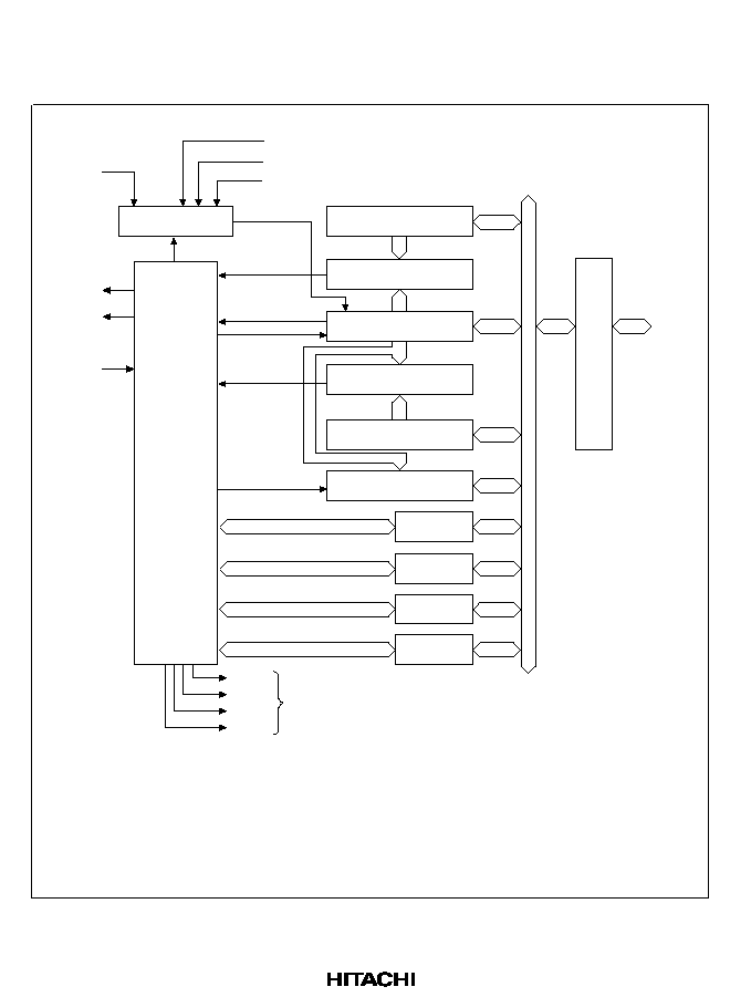
296
11.1.2
Block Diagram
Figure 11.1 shows a block diagram of the FRT.
FTI
/8
Internal clock
Internal
data bus
Module
data bus
/32
/128
ICI
Interrupt
signals
OCIA
OCIB
OVI
FTOB
FTOA
FTCI
Control
logic
Clock select
Clock
Compare
match A
Overflow
Clear
Compare
match B
Capture
OCRA (H/L)
Comparator A
FRC (H/L)
Comparator B
OCRB (H/L)
ICR (H/L)
FTCSR
TIER
TCR
TOCR
Bus interface
OCRA,B: Output compare registers A,B (16 bits)
FRC: Free-running counter (16 bits)
ICR: Input capture register (16 bits)
TCR: Timer control register (8 bits)
TIER: Timer interrupt enable register (8 bits)
FTCSR: Free-running timer control/status register (8 bits)
TOCR: Timer output compare control register (8 bits)
Figure 11.1 FRT Block Diagram

297
11.1.3
Pin Configuration
Table 11.1 lists FRT I/O pins and their functions.
Table 11.1
Pin Configuration
Channel
Pin
I/O
Function
Counter clock input pin
FTCI
I
FRC counter clock input pin
Output compare A output pin
FTOA
O
Output pin for output compare A
Output compare B output pin
FTOB
O
Output pin for output compare B
Input capture input pin
FTI
I
Input pin for input capture
11.1.4
Register Configuration
Table 11.2 shows the FRT register configuration.
Table 11.2
Register Configuration
Register
Abbreviation
R/W
Initial
Value
Address
Timer interrupt enable register
TIER
R/W
H'01
HFFFFFE10
Free-running timer control/status register
FTCSR
R/(W)*
1
H'00
HFFFFFE11
Free-running counter H
FRC H
R/W
H'00
HFFFFFE12
Free-running counter L
FRC L
R/W
H'00
HFFFFFE13
Output compare register A H
OCRA H
R/W
H'FF
HFFFFFE14*
2
Output compare register A L
OCRA L
R/W
H'FF
HFFFFFE15*
2
Output compare register B H
OCRB H
R/W
H'FF
HFFFFFE14*
2
Output compare register B L
OCRB L
R/W
H'FF
HFFFFFE15*
2
Timer control register
TCR
R/W
H'00
HFFFFFE16
Timer output compare control register
TOCR
R/W
H'E0
HFFFFFE17
Input capture register H
ICR H
R
H'00
HFFFFFE18
Input capture register L
ICR L
R
H'00
HFFFFFE19
Notes: 1. Bits 7 to 1 are read-only. The only value that can be written is a 0, which is used to
clear flags. Bit 0 can be read or written.
2. OCRA and OCRB have the same address. The OCRS bit in TOCR is used to switch
between them.
3. Use byte-size access for all registers.

298
11.2
Register Descriptions
11.2.1
Free-Running Counter (FRC)
Bit:
15
14
13
...
3
2
1
0
Bit name:
...
Initial value:
0
0
0
...
0
0
0
0
R/W:
R/W
R/W
R/W
...
R/W
R/W
R/W
R/W
FRC is a 16-bit read/write up-counter. It increments upon input of a clock. The input clock can be
selected using clock select bits 1 and 0 (CKS1, CKS0) in TCR. FRC can be cleared upon compare
match A.
When FRC overflows (H'FFFF
H'0000), the overflow flag (OVF) in FTCSR is set to 1. FRC
can be read or written to by the CPU, but because it is 16 bits long, data transfers involving the
CPU are performed via a temporary register (TEMP). See section 11.3, CPU Interface, for more
detailed information.
FRC is initialized to H'0000 by a reset, in standby mode, and when the module standby function is
used.
11.2.2
Output Compare Registers A and B (OCRA and OCRB)
Bit:
15
14
13
...
3
2
1
0
Bit name:
...
Initial value:
1
1
1
...
1
1
1
1
R/W:
R/W
R/W
R/W
...
R/W
R/W
R/W
R/W
OCR is composed of two 16-bit read/write registers (OCRA and OCRB). The contents of OCR are
always compared to the FRC value. When the two values are the same, the output compare flags
in FTCSR (OCFA and OCFB) are set to 1.
When the OCR and FRC values are the same (compare match), the output level values set in the
output level bits (OLVLA and OLVLB) are output to the output compare pins (FTOA and FTOB).
After a reset, FTOA and FTOB output 0 until the first compare match occurs.
Because OCR is a 16-bit register, data transfers involving the CPU are performed via a temporary
register (TEMP). See section 11.3, CPU Interface, for more detailed information.
OCR is initialized to H'FFFF by a reset, in standby mode, and when the module standby function
is used.

299
11.2.3
Input Capture Register (ICR)
Bit:
15
14
13
...
3
2
1
0
Bit name:
...
Initial value:
0
0
0
...
0
0
0
0
R/W:
R
R
R
...
R
R
R
R
ICR is a 16-bit read-only register. When a rising edge or falling edge of the input capture signal is
detected, the current FRC value is transferred to ICR. At the same time, the input capture flag
(ICF) in FTCSR is set to 1. The edge of the input signal can be selected using the input edge select
bit (IEDGA) in TCR.
Because ICR is a 16-bit register, data transfers involving the CPU are performed via a temporary
register (TEMP). See Section 11.3, CPU Interface, for more detailed information. To ensure that
the input capture operation is reliably performed, set the pulse width of the input capture input
signal to six system clocks (
) or more.
ICR is initialized to H'0000 by a reset, in standby mode, and when the module standby function is
used.
11.2.4
Timer Interrupt Enable Register (TIER)
Bit:
7
6
5
4
3
2
1
0
Bit name:
ICIE
--
--
--
OCIAE
OCIBE
OVIE
--
Initial value:
0
0
0
0
0
0
0
1
R/W:
R/W
--
--
--
R/W
R/W
R/W
--
TIER is an 8-bit read/write register that controls enabling of all interrupt requests. TIER is
initialized to H'01 by a reset, in standby mode, and when the module standby function is used.
·
Bit 7--Input Capture Interrupt Enable (ICIE): Selects enabling/disabling of the ICI interrupt
request when the input capture flag (ICF) in FTCSR is set to 1.
Bit 7: ICIE
Description
0
Interrupt request (ICI) caused by ICF disabled
(Initial value)
1
Interrupt request (ICI) caused by ICF enabled
·
Bits 6 to 4--Reserved: These bits always read 0. The write value should always be 0. Do not
write 1.

300
·
Bit 3--Output Compare Interrupt A Enable (OCIAE): Selects enabling/disabling of the OCIA
interrupt request when the output compare flag A (OCFA) in FTCSR is set to 1.
Bit 3: OCIAE
Description
0
Interrupt request (OCIA) caused by OCFA disabled
(Initial value)
1
Interrupt request (OCIA) caused by OCFA enabled
·
Bit 2--Output Compare Interrupt B Enable (OCIBE): Selects enabling/disabling of the OCIB
interrupt request when the output compare flag B (OCFB) in FTCSR is set to 1.
Bit 2: OCIBE
Description
0
Interrupt request (OCIB) caused by OCFB disabled
(Initial value)
1
Interrupt request (OCIB) caused by OCFB enabled
·
Bit 1--Timer Overflow Interrupt Enable (OVIE): Selects enabling/disabling of the OVI
interrupt request when the overflow flag (OVF) in FTCSR is set to 1.
Bit 1: OVIE
Description
0
Interrupt request (FOVI) caused by OVF disabled
(initial value)
1
Interrupt request (FOVI) caused by OVF enabled
·
Bit 0--Reserved: This bit always reads 1. The write value should always be 1.
11.2.5
Free-Running Timer Control/Status Register (FTCSR)
Bit:
7
6
5
4
3
2
1
0
Bit name:
ICF
--
--
--
OCFA
OCFB
OVF
CCLRA
Initial value:
0
0
0
0
0
0
0
0
R/W:
R/(W)*
--
--
--
R/(W)*
R/(W)*
R/(W)*
R/W
Note: For bits 7, and 3 to 1, the only value that can be written is 0 (to clear the flags).
FTCSR is an 8-bit register that selects counter clearing and controls interrupt request signals.
FTCSR is initialized to H'00 by a reset, in standby mode, and when the module standby function is
used. See section 11.4, Operation, for the timing.
·
Bit 7--Input Capture Flag (ICF): Status flag that indicates that the FRC value has been sent to
FICR by the input capture signal. This flag is cleared by software and set by hardware. It
cannot be set by software.

301
Bit 7: ICF
Description
0
Clear conditions: When ICF is read while set to 1, and then 0 is
written to it
(Initial value)
1
Set conditions: When the FRC value is sent to ICR by the input
capture signal
·
Bits 6 to 4--Reserved: These bits always read 0. The write value should always be 0.
·
Bit 3--Output Compare Flag A (OCFA): Status flag that indicates when the values of the FRC
and OCRA match. This flag is cleared by software and set by hardware. It cannot be set by
software.
Bit 3: OCFA
Description
0
Clear conditions: When OCFA is read while set to 1, and then 0 is
written to it
(Initial value)
1
Set conditions: When the FRC value becomes equal to OCRA
·
Bit 2--Output Compare Flag B (OCFB): Status flag that indicates when the values of FRC and
OCRB match. This flag is cleared by software and set by hardware. It cannot be set by
software.
Bit 2: OCFB
Description
0
Clear conditions: When OCFB is read while set to 1, and then 0 is
written to it
(Initial value)
1
Set conditions: When the FRC value becomes equal to OCRB
·
Bit 1--Timer Overflow Flag (OVF): Status flag that indicates when FRC overflows (from
H'FFFF to H'0000). This flag is cleared by software and set by hardware. It cannot be set by
software.
Bit 1: OVF
Description
0
Clear conditions: When OVF is read while set to 1, and then 0 is
written to it
(Initial value)
1
Set conditions: When the FRC value changes from H'FFFF to H'0000
·
Bit 0--Counter Clear A (CCLRA): Selects whether or not to clear FRC on compare match A
(signal indicating match of FRC and OCRA).

302
Bit 0: CCLRA
Description
0
FRC clear disabled
(Initial value)
1
FRC cleared on compare match A
11.2.6
Timer Control Register (TCR)
Bit:
7
6
5
4
3
2
1
0
Bit name:
IEDGA
--
--
--
--
--
CKS1
CKS0
Initial value:
0
0
0
0
0
0
0
0
R/W:
R/W
R/W
R/W
R/W
R/W
R/W
R/W
R/W
TCR is an 8-bit read/write register that selects the input edge for input capture and selects the
input clock for FRC. TCR is initialized to H'00 by a reset, in standby mode, and when the module
standby function is used.
·
Bit 7--Input Edge Select (IEDG): Selects whether to capture the input capture input (FTI) on
the falling edge or rising edge.
Bit 7: IEDG
Description
0
Input captured on falling edge
(Initial value)
1
Input captured on rising edge
·
Bits 6 to 2--Reserved: These bits always read 0. The write value should always be 0. Do not
write 1.
·
Bits 1 and 0--Clock Select (CKS1, CKS0): These bits select whether to use an external clock
or one of three internal clocks for input to FRC. The external clock is counted at the rising
edge.
Bit 1: CKS1
Bit 0: CKS0
Description
0
0
Internal clock: count at
/8
(Initial value)
1
Internal clock: count at
/32
1
0
Internal clock: count at
/128
1
External clock: count at rising edge

303
11.2.7
Timer Output Compare Control Register (TOCR)
Bit:
7
6
5
4
3
2
1
0
Bit name:
--
--
--
OCRS
--
--
OLVLA
OLVLB
Initial value:
1
1
1
0
0
0
0
0
R/W:
--
--
--
R/W
R/W
R/W
R/W
R/W
TOCR is an 8-bit read/write register that selects the output level for output compare, enables
output compare output, and controls switching between access of output compare registers A and
B. TOCR is initialized to H'E0 by a reset, in standby mode, and when the module standby function
is used.
Bits 7 to 5--Reserved: These bits always read 1. The write value should always be 1. Do not write
0.
Bit 4--Output Compare Register Select (OCRS): OCRA and OCRB share the same address. The
OCRS bit controls which register is selected when reading/writing to this address. It does not
affect the operation of OCRA and OCRB.
Bit 4: OCRS
Description
0
OCRA register selected
(Initial value)
1
OCRB register selected
Bits 3 and 2--Reserved: These bits always read 0. The write value should always be 0. Do not
write 1.
Bit 1--Output Level A (OLVLA): Selects the level output to the output compare A output pin
upon compare match A (signal indicating match of FRC and OCRA).
Bit 1: OLVLA
Description
0
0 output on compare match A
(Initial value)
1
1 output on compare match A
Bit 0--Output Level B (OLVLB): Selects the level output to the output compare B output pin
upon compare match B (signal indicating match of FRC and OCRB).
Bit 0: OLVLB
Description
0
0 output on compare match B
(Initial value)
1
1 output on compare match B

304
11.3
CPU Interface
FRC, OCRA, OCRB, and FICR are 16-bit registers. The data bus width between the CPU and
FRT, however, is only 8 bits. Access of these three types of registers from the CPU therefore
needs to be performed via an 8-bit temporary register called TEMP.
The following describes how these registers are read from and written to:
·
Writing to 16-bit Registers
The upper byte is written, which results in the upper byte of data being stored in TEMP. The
lower byte is then written, which results in 16 bits of data being written to the register when
combined with the upper byte value in TEMP.
·
Reading from 16-bit Registers
The upper byte of data is read, which results in the upper byte value being transferred to the
CPU. The lower byte value is transferred to TEMP. The lower byte is then read, which results
in the lower byte value in TEMP being sent to the CPU.
When registers of these three types are accessed, two byte accesses should always be performed,
first to the upper byte, then the lower byte. The same applies to accesses with the on-chip direct
memory access controller. If only the upper byte or lower byte is accessed, the data will not be
transferred properly.
Figure 11.2 and 11.3 show the flow of data when FRC is accessed. Other registers function in the
same way. When reading OCRA and OCRB, however, both upper and lower-byte data is
transferred directly to the CPU without passing through TEMP.
305
CPU
(H'AA)
upper
byte
Data bus within module
Bus interface
TEMP
(H'AA)
FRC H
( )
FRC L
( )
(Write to upper byte)
CPU
(H'55)
lower
byte
Data bus within module
Bus interface
TEMP
(H'AA)
FRC H
(H'AA)
FRC L
(H'55)
(Write to lower byte)
Figure 11.2 FRC Access Operation (CPU Writes H'AA55 to FRC)
306
CPU
(H'AA)
upper
byte
TEMP
(H'55)
FRC H
(H'AA)
FRC L
(H'55)
Data bus within module
Bus interface
(Read from upper byte)
CPU
(H'55)
lower
byte
TEMP
(H'AA)
FRC H
( )
FRC L
( )
Data bus within module
Bus interface
(Read from lower byte)
Figure 11.3 FRC Access Operation (CPU Reads H'AA55 from FRC)
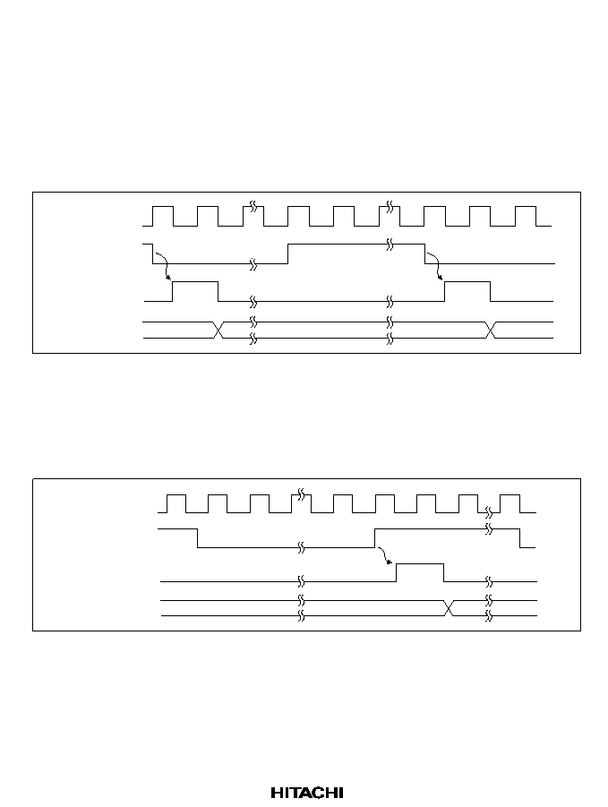
307
11.4
Operation
11.4.1
FRC Count Timing
The FRC increments on clock input (internal or external).
Internal Clock Operation: Set the CKS1 and CKS0 bits in TCR to select which of the three
internal clocks created by dividing system clock
(
/8,
/32,
/128) is used. Figure 11.4 shows
the timing.
Timer drive
clock
N 1
N
N + 1
Internal clock
FRC input
clock
FRC
Figure 11.4 Count Timing (Internal Clock Operation)
External Clock Operation: Set the CKS1 and CKS0 bits in TCR to select the external clock.
External clock pulses are counted on the rising edge. The pulse width of the external clock must be
at least 6 system clocks (
). A smaller pulse width will result in inaccurate operation. Figures 11.5
shows the timing.
Timer drive
clock
N
N + 1
External clock
input pin
FRC input
clock
FRC
Figure 11.5 Count Timing (External Clock Operation)
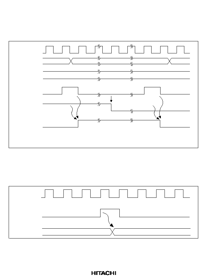
308
11.4.2
Output Timing for Output Compare
When a compare match occurs, the output level set in the OLVL bit in TOCR is output from the
output compare output pins (FTOA, FTOB). Figure 11.6 shows the timing for output of output
compare A.
Clear*
N
N
N
N
N + 1
N + 1
Timer drive
clock
FRC
OCRA
Compare
match A
signal
OLVLA
Output
compare A
output pin
FTOA
Note:
Indicates instruction execution by software
Figure 11.6 Output Timing for Output Compare A
11.4.3
FRC Clear Timing
FRC can be cleared on compare match A. Figure 11.7 shows the timing.
Timer drive
clock
Compare
match A
signal
FRC
N
H'0000
Figure 11.7 Compare Match A Clear Timing
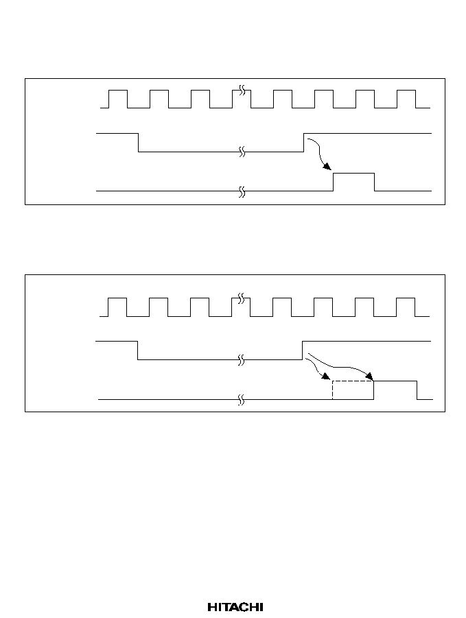
309
11.4.4
Input Capture Input Timing
Either the rising edge or falling edge, can be selected for input capture input using the IEDG bit in
TCR. Figure 11.8 shows the timing when the rising edge is selected (IEDG = 1).
Timer drive
clock
Input capture
input pin
Input capture
signal
Figure 11.8 Input Capture Signal Timing (Normal)
When the input capture signal is input when ICR is read (upper-byte read), the input capture signal
is delayed by one cycle of the clock that drives the timer. Figure 11.9 shows the timing.
Timer drive
clock
Input capture
input pin
Input capture
signal
ICR upper-byte read cycle
Figure 11.9 Input Capture Signal Timing (Input Capture Input when ICR is Read)
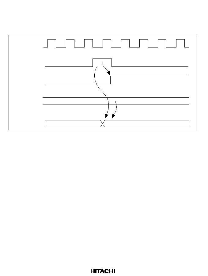
310
11.4.5
Input Capture Flag (ICF) Setting Timing
Input capture input sets the input capture flag (ICF) to 1 and simultaneously transfers the FRC
value to ICR. Figure 11.10 shows the timing.
Timer drive
clock
Input capture
signal
ICF
FRC
ICR
N
N
Figure 11.10 ICF Setting Timing
11.4.6
Output Compare Flag (OCFA, OCFB) Setting Timing
The compare match signal output (when OCRA or OCRB matches the FRC value) sets output
compare flag OCFA or OCFB to 1. The compare match signal is generated in the last state in
which the values matched (at the timing for updating the count value that matched the FRC). After
OCRA or OCRB matches the FRC, no compare match signal is generated until the increment lock
is generated. Figure 11.11 shows the timing for setting OCFA and OCFB.
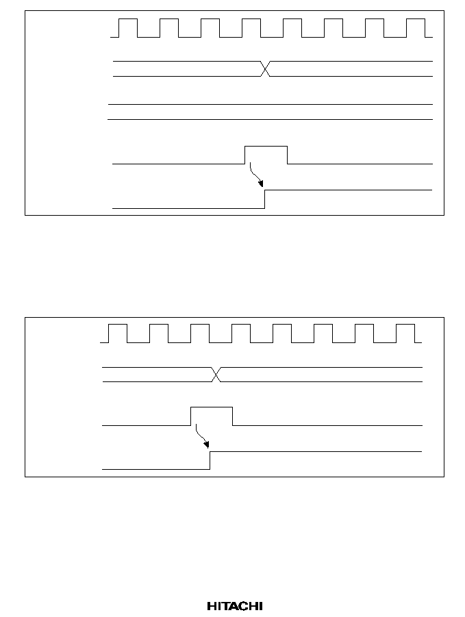
311
Timer drive
clock
FRC
OCRA, OCRB
Compare match
signal
OCFA, OCFB
N + 1
N
N
Figure 11.11 OCF Setting Timing
11.4.7
Timer Overflow Flag (OVF) Setting Timing
FRC overflow (from H'FFFF to H'0000) sets the timer overflow flag (OVF) to 1. Figure 11.12
shows the timing.
Timer drive
clock
FRC
Overflow
signal
OVF
H'0000
H'FFFF
Figure 11.12 OVF Setting Timing
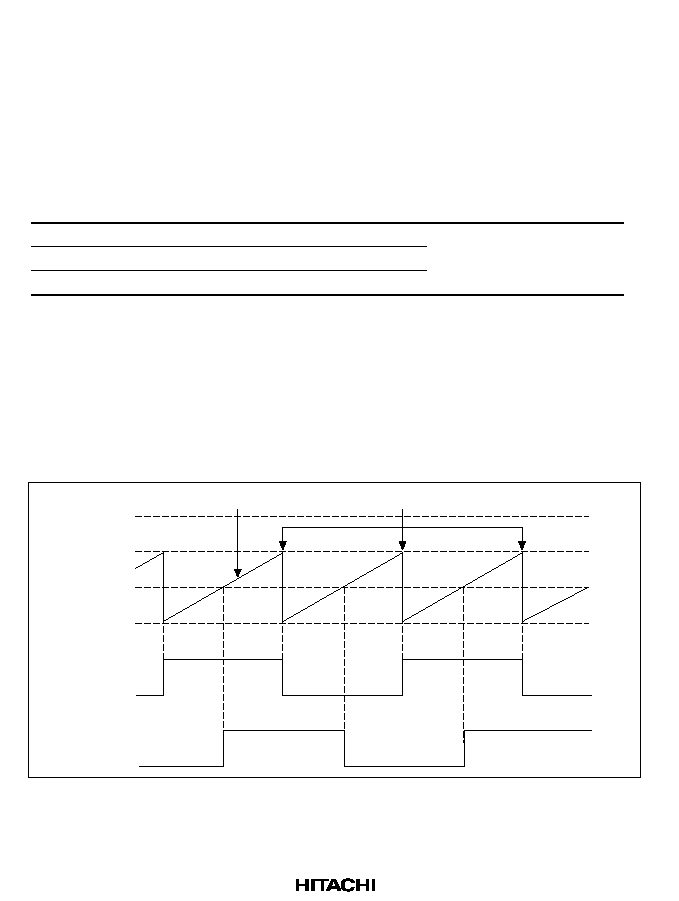
312
11.5
Interrupt Sources
There are four FRT interrupt sources of three types (ICI, OCIA/OCIB, and OVI). Table 11.3 lists
the interrupt sources and their priorities after a reset is cleared. The interrupt enable bits in TIER
are used to enable or disable the interrupt bits. Each interrupt request is sent to the interrupt
controller independently. See section 4, Exception Handling, for more information about priorities
and the relationship to interrupts other than those of the FRT.
Table 11.3
FRT Interrupt Sources and Priorities
Interrupt Source
Description
Priority
ICI
Interrupt by ICF
High
OCIA, OCIB
Interrupt by OCFA or OCFB
OVI
Interrupt by OVF
Low
11.6
Example of FRT Use
Figure 11.13 shows an example in which pulses with a 50% duty factor and arbitrary phase
relationship are output. The procedure is as follows:
1. Set the CCLRA bit in FTCSR to 1.
2. The OLVLA and OLVLB bits are inverted by software whenever a compare match occurs.
H'FFFF
OCRA
OCRB
H'0000
FTOA
FTOB
FRC
Counter clear
Figure 11.13 Example of Pulse Output
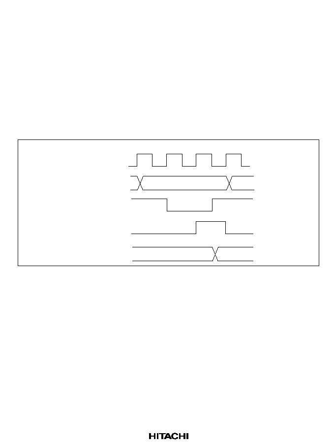
313
11.7
Usage Notes
Note that the following contention and operations occur when the FRT is operating:
1. FRC operates on the timer drive clock (
/4), which has a cycle of 4 times the system clock (
).
For this reason, when the CPU performs an access, both the CPU and FRT will be operating,
so a WAIT request will be generated from the FRT to the CPU. The number of access cycles
thus varies by between 3 and 12 cycles.
2. Contention between FRC Write and Clear
When a counter clear signal is generated with the timing shown in figure 11.14 during the
write cycle for the lower byte of FRC, writing does not occur to the FRC, and the FRC clear
takes priority.
Timer drive
clock
FRC lower-byte write cycle
Address
Internal write
signal
Counter clear
signal
FRC
FRC address
N
H'0000
Figure 11.14 Contention between FRC Write and Clear
3. Contention between FRC Write and Increment
When an increment occurs with the timing shown in figure 11.15 during the write cycle for the
lower byte of FRC, no increment is performed and the counter write takes priority.
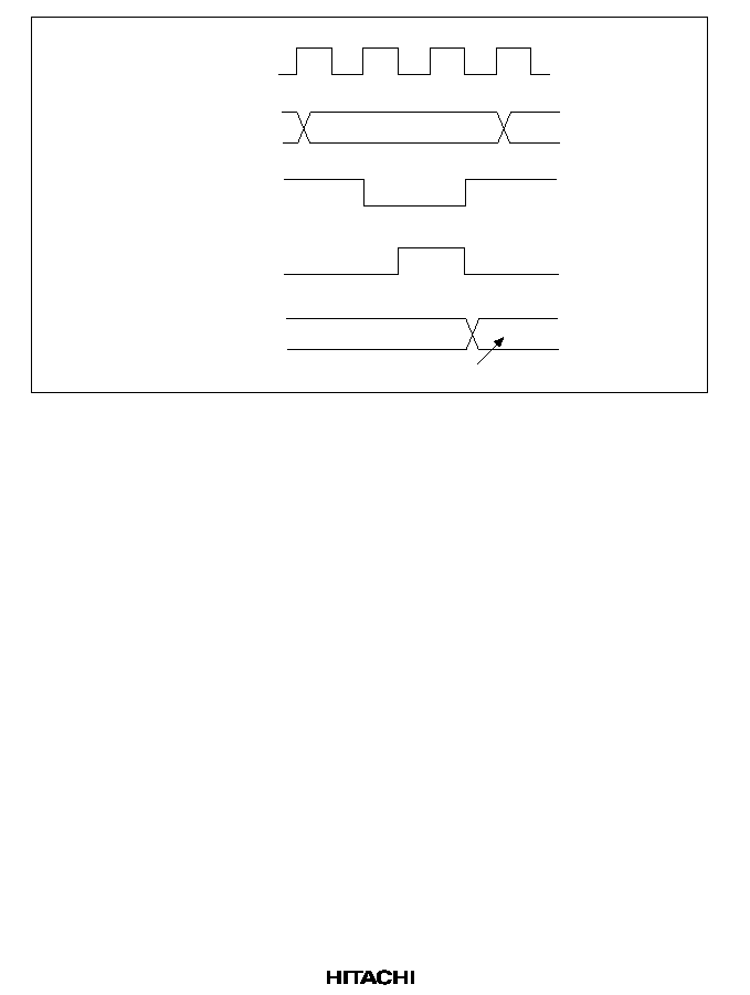
314
FRC
FRC address
N
M
Write data
Timer drive
clock
FRC upper-byte write cycle
Address
Internal write
signal
FRC input
clock
Figure 11.15 Contention between FRC Write and Increment
4. Contention between OCR Write and Compare Match
When a compare match occurs with the timing shown in figure 11.16, during the write cycle
for the lower byte of OCRA or OCRB, the OCR write takes priority and the compare match
signal is disabled.
315
FRC
Compare match
signal
OCR
OCR address
N
M
N
N + 1
Write data
Disabled
Timer drive
clock
FRC lower-byte write cycle
Address
Internal write
signal
Figure 11.16 Contention between OCR and Compare Match
5. Internal Clock Switching and Counter Operation
FRC will sometimes begin incrementing because of the timing of switching between internal
clocks. Table 11.4 shows the relationship between internal clock switching timing (CKS1 and
CKS0 bit rewrites) and FRC operation.
When an internal clock is used, the FRC clock is generated when the falling edge of an internal
clock (created by dividing the system clock (
)) is detected. When a clock is switched to high
before the switching and to low after switching, as shown in case 3 in table 11.4, the
switchover is considered a falling edge and an FRC clock pulse is generated, causing FRC to
increment. FRC may also increment when switching between an internal clock and an external
clock.
316
Table 11.4
Internal Clock Switching and FRC Operation
No.
Timing of Rewrite of
CKS1 and CKS0 Bits
FRC Operation
1
Low-to-low switch
Clock before
switching
Clock after
switching
FRC clock
FRC
N
N + 1
Rewrite of CKS bit
2
Low-to-high switch
N
N + 1
N + 2
Clock before
switching
Clock after
switching
FRC clock
FRC
Rewrite of CKS bit
317
Table 11.4
Internal Clock Switching and FRC Operation (cont)
No.
Timing of Rewrite of
CKS1 and CKS0 Bits
FRC Operation
3
High-to-low switch
N
N + 1
N + 2
Clock before
switching
Clock after
switching
FRC clock
FRC
Rewrite of CKS bit
4
High-to-high switch
N
N + 1
N + 2
Clock before
switching
Clock after
switching
FRC clock
FRC
Rewrite of CKS bit
Note:
Because the switchover is considered a falling edge, FRC starts counting up.
6. Timer Output (FTOA, FTOB)
During a power-on reset, the timer outputs (FTOA, FTOB) will be unreliable until the
oscillation stabilizes. The initial value is output after the oscillation settling time has elapsed.

318

319
Section 12 Watchdog Timer (WDT)
12.1
Overview
The SH7604 has a single-channel watchdog timer (WDT) for monitoring system operations. If a
system becomes uncontrolled and the timer counter overflows without being rewritten correctly by
the CPU, an overflow signal (
WDTOVF) is output externally. The WDT can simultaneously
generate an internal reset signal for the entire chip.
When this watchdog function is not needed, the WDT can be used as an interval timer. In the
interval timer operation, an interval timer interrupt is generated at each counter overflow. The
WDT is also used when recovering from standby mode, in modifying a clock frequency, and in
clock pause mode.
12.1.1
Features
·
Works in watchdog timer mode or interval timer mode.
·
Outputs
WDTOVF in watchdog timer mode. When the counter overflows in watchdog timer
mode, overflow signal
WDTOVF is output externally. It is possible to select whether to reset
the chip internally when this happens. Either the power-on reset or manual reset signal can be
selected as the internal reset signal.
·
Generates interrupts in interval timer mode. When the counter overflows, it generates an
interval timer interrupt.
·
Used for standby mode clearing, clock frequency modification, and clock pause mode.
·
Works with eight counter clock sources.
320
12.1.2
Block Diagram
Figure 12.1 shows a block diagram of the WDT.
/2
/64
/128
/256
/512
/1024
/4096
/8192
Internal
clock
Clock
Overflow
Clock
select
Interrupt
control
Reset
control
RSTCSR
TCNT
TCSR
Module bus
Bus
interface
Interna bus
ITI
(interrupt
request signal)
WDTOVF
Internal
reset signal*
WDT
WTCSR:
Watchdog timer control/status register
WTCNT:
Watchdog timer counter
RSTCSR:
Reset control/status register
Note: The internal reset signal can be generated by a register setting. The type of reset can be
selected (power-on or manual reset).
Figure 12.1 WDT Block Diagram
12.1.3
Pin Configuration
Table 12.1 shows the pin configuration.
Table 12.1
Pin Configuration
Pin
Abbreviation
I/O
Function
Watchdog timer overflow
WDTOVF
O
Outputs the counter overflow signal in
watchdog mode

321
12.1.4
Register Configuration
Table 12.2 summarizes the three WDT registers. They are used to select the clock, switch the
WDT mode, and control the reset signal.
Table 12.2
WDT Registers
Address
Name
Abbreviation
R/W
Initial Value
Write
*1
Read*
2
Watchdog timer
control/status register
WTCSR
R/(W)*
3
H'18
H'FFFFFE80
H'FFFFFE80
Watchdog timer
counter
WTCNT
R/W
H'00
H'FFFFFE80
H'FFFFFE81
Reset control/status
register
RSTCSR
R/(W)*
3
H'1F
H'FFFFFE82
H'FFFFFE83
Notes: 1. Write by word access. It cannot be written by byte or longword access.
2. Read by byte access. The correct value cannot be read by word or longword access.
3. Only 0 can be written in bit 7 to clear the flag.
12.2
Register Descriptions
12.2.1
Watchdog Timer Counter (WTCNT)
WTCNT is an 8-bit read/write up-counter. WTCNT differs from other registers in that it is more
difficult to write. See section 12.2.4, Register Access, for details. When the timer enable bit
(TME) in the watchdog timer control/status register (WTCSR) is set to 1, the watchdog timer
counter starts counting pulses of an internal clock source selected by clock select bits 2 to 0
(CKS2 to CKS0) in WTCSR. When the value of WTCNT overflows (changes from H'FF to H'00),
a watchdog timer overflow signal (
WDTOVF) or interval timer interrupt (ITI) is generated,
depending on the mode selected in the WT/
IT bit in WTCSR. WTCNT is initialized to H'00 by a
reset and when the TME bit is cleared to 0. It is not initialized in standby mode.
Bit:
7
6
5
4
3
2
1
0
Bit name:
Initial value:
0
0
0
0
0
0
0
0
R/W:
R/W
R/W
R/W
R/W
R/W
R/W
R/W
R/W

322
12.2.2
Watchdog Timer Control/Status Register (WTCSR)
The watchdog timer control/status register (WTCSR) is an 8-bit read/write register. WTCSR
differs from other registers in being more difficult to write. See section 12.2.4, Register Access,
for details. Its functions include selecting the timer mode and clock source. Bits 7 to 5 are
initialized to 000 by a reset and in standby mode. Bits 2 to 0 are initialized to 000 by a reset, but
retain their values in standby mode.
Bit:
7
6
5
4
3
2
1
0
Bit name:
OVF
WT/
IT
TME
--
--
CKS2
CKS1
CKS0
Initial value:
0
0
0
1
1
0
0
0
R/W:
R/(W)
R/W
R/W
--
--
R/W
R/W
R/W
·
Bit 7--Overflow Flag (OVF): Indicates that WTCNT has overflowed from H'FF to H'00. It is
not set in watchdog timer mode.
Bit 7: OVF
Description
0
No overflow of WTCNT in interval timer mode
(Initial value)
Cleared by reading OVF, then writing 0 in OVF
1
WTCNT overflow in interval timer mode
·
Bit 6--Timer Mode Select (WT/
IT): Selects whether to use the WDT as a watchdog timer or
interval timer. When WTCNT overflows, the WDT either generates an interval timer interrupt
(ITI) or generates a
WDTOVF signal, depending on the mode selected.
Bit 6: WT/
IT
Description
0
Interval timer mode: interval timer interrupt (ITI) request to the CPU
when WTCNT overflows
(Initial value)
1
Watchdog timer mode:
WDTOVF
signal output externally when WTCNT
overflows. Section 12.2.3, Reset Control/Status Register (RSTCSR),
describes in detail what happens when WTCNT overflows in watchdog
timer mode.
·
Bit 5--Timer Enable (TME): Enables or disables the timer.
Bit 5: TME
Description
0
Timer disabled: WTCNT is initialized to H'00 and count-up stops
(Initial value)
1
Timer enabled: WTCNT starts counting. A
WDTOVF
signal or interrupt
is generated when WTCNT overflows.
323
·
Bits 4 and 3--Reserved: These bits always read 1. The write value shoul always be 1.
·
Bits 2 to 0--Clock Select 2 to 0 (CKS2 to CKS0): These bits select one of eight internal clock
sources for input to WTCNT. The clock signals are obtained by dividing the frequency of the
system clock (
).
Description
Bit 2: CKS2 Bit 1: CKS1 Bit 0: CKS0 Clock Source
Overflow Interval* (
= 28.7 MHz)
0
0
0
/2 (Initial value)
17.8
µ
s
0
0
1
/64
570.8
µ
s
0
1
0
/128
1.1 ms
0
1
1
/256
2.2 ms
1
0
0
/512
4.5 ms
1
0
1
/1024
9.1 ms
1
1
0
/4096
36.5 ms
1
1
1
/8192
73.0 ms
Note:
The overflow interval listed is the time from when the WTCNT begins counting at H'00 until
an overflow occurs.
12.2.3
Reset Control/Status Register (RSTCSR)
RSTCSR is an eight-bit read/write register that controls output of the reset signal generated by
watchdog timer counter (WTCNT) overflow and selects the internal reset signal type. RSTCSR
differs from other registers in that it is more difficult to write. See section 12.2.4, Register Access,
for details. RSTCR is initialized to H'1F by input of a reset signal from the
RES pin, but is not
initialized by the internal reset signal generated by overflow of the WDT. It is initialized to H'1F
in standby mode.
Bit:
7
6
5
4
3
2
1
0
Bit name:
WOVF
RSTE
RSTS
--
--
--
--
--
Initial value:
0
0
0
1
1
1
1
1
R/W:
R/(W)*
R/W
R/W
--
--
--
--
--
Note:
Only 0 can be written in bit 7 to clear the flag.
·
Bit 7--Watchdog Timer Overflow Flag (WOVF): Indicates that WTCNT has overflowed
(from H'FF to H'00) in watchdog timer mode. It is not set in interval timer mode.

324
Bit 7: WOVF
Description
0
No WTCNT overflow in watchdog timer mode
(Initial value)
Cleared by reading WOVF, then writing 0 in WOVF
1
Set by WTCNT overflow in watchdog timer mode
·
Bit 6--Reset Enable (RSTE): Selects whether to reset the chip internally if WTCNT overflows
in watchdog timer mode.
Bit 6: RSTE
Description
0
Not reset when WTCNT overflows
(Initial value)
LSI not reset internally, but WTCNT and WTCSR reset within WDT
1
Reset when WTCNT overflows
·
Bit 5--Reset Select (RSTS): Selects the type of internal reset generated if WTCNT overflows
in watchdog timer mode.
Bit 5: RSTS
Description
0
Power-on reset
(Initial value)
1
Manual reset
·
Bits 4 to 0--Reserved: These bits always read as 1. The write value should always be 1.
12.2.4
Register Access
The watchdog timer's WTCNT, WTCSR, and RSTCSR registers differ from other registers in that
they are more difficult to write. The procedures for writing and reading these registers are given
below.
Writing to WTCNT and WTCSR: These registers must be written by a word transfer
instruction. They cannot be written by byte or longword transfer instructions. WTCNT and
WTCSR both have the same write address. The write data must be contained in the lower byte of
the written word. The upper byte must be H'5A (for WTCNT) or H'A5 (for WTCSR) (figure 12.2).
This transfers the write data from the lower byte to WTCNT or WTCSR.
325
Writing to WTCNT
15
8 7
0
Address:
H'FFFFFE80
H'5A
Write data
Writing to WTCSR
15
8 7
0
Address:
H'FFFFFE80
H'A5
Write data
Figure 12.2 Writing to WTCNT and WTCSR
Writing to RSTCSR: RSTCSR must be written by a word access to address H'FFFFFE82. It
cannot be written by byte or longword transfer instructions. Procedures for writing 0 in WOVF
(bit 7) and for writing to RSTE (bit 6) and RSTS (bit 5) are different, as shown in figure 12.3. To
write 0 in the WOVF bit, the write data must be H'A5 in the upper byte and H'00 in the lower byte.
This clears the WOVF bit to 0. The RSTE and RSTS bits are not affected. To write to the RSTE
and RSTS bits, the upper byte must be H'5A and the lower byte must be the write data. The values
of bits 6 and 5 of the lower byte are transferred to the RSTE and RSTS bits, respectively. The
WOVF bit is not affected.
Writing 0 to the WOVF bit
15
8 7
0
Address:
H'FFFFFE82
H'A5
H'00
Writing to the RSTE and RSTS bits
15
8 7
0
Address:
H'FFFFFE82
H'5A
Write data
Figure 12.3 Writing to RSTCSR
Reading from WTCNT, WTCSR, and RSTCSR: WTCNT, WTCSR, and RSTCSR are read
like other registers. Use byte transfer instructions. The read addresses are H'FFFFFE80 for
WTCSR, H'FFFFFE81 for WTCNT, and H'FFFFFE83 for RSTCSR.

326
12.3
Operation
12.3.1
Operation in Watchdog Timer Mode
To use the WDT as a watchdog timer, set the WT/
IT and TME bits in WTCSR to 1. Software
must prevent WTCNT overflow by rewriting the WTCNT value (normally by writing H'00) before
overflow occurs. If WTCNT fails to be rewritten and overflows occur due to a system crash or the
like, a
WDTOVF signal is output (figure 12.4). The WDTOVF signal can be used to reset the
system. The
WDTOVF signal is output for 128
clock cycles.
If the RSTE bit in RSTCSR is set to 1, a signal to reset the chip will be generated internally
simultaneously with the
WDTOVF signal when WTCNT overflows. Either a power-on reset or a
manual reset can be selected by the RSTS bit. The internal reset signal is output for 512
clock
cycles.
When a watchdog reset is generated simultaneously with input at the
RES pin, the software
distinguishes the
RES reset from the watchdog reset by checking the WOVF bit in RSTCSR. The
RES reset takes priority. The WOVF bit is cleared to 0.
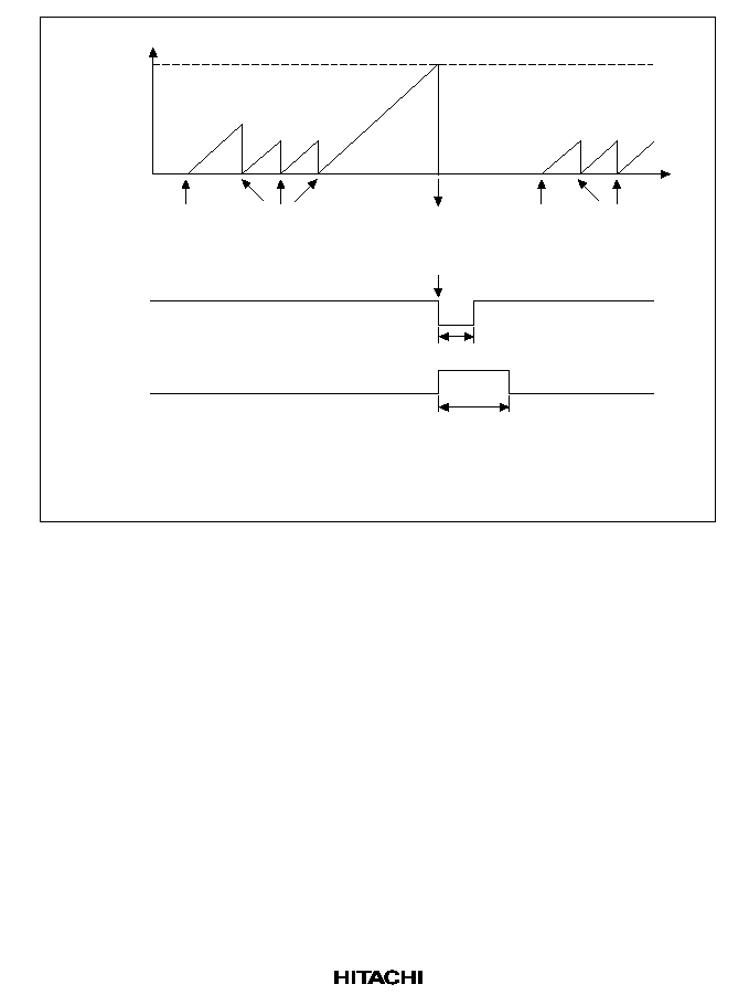
327
WOVF = 1
WTCNT value
Overflow
WT/
IT
= 1
TME = 1
WT/
IT
= 1
TME = 1
H'00 written
in WTCNT
H'00 written
in WTCNT
WDTOVF
and
internal reset generated
H'FF
H'00
128
clocks
512
clocks
WDTOVF
signal
Internal
reset
signal*
Time
WT/
IT
: Timer mode select bit
TME: Timer enable bit
Note: Internal reset signal is generated only when the RSTE bit is set to 1.
Figure 12.4 Operation in Watchdog Timer Mode
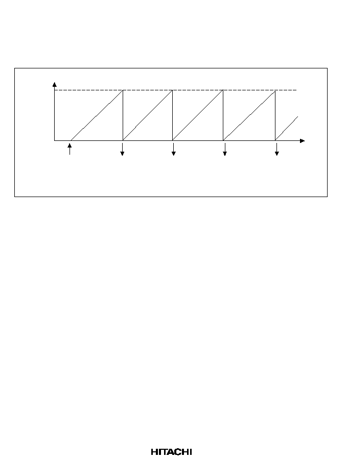
328
12.3.2
Operation in Interval Timer Mode
To use the WDT as an interval timer, clear WT/
IT to 0 and set TME to 1 in WTSCR. An interval
timer interrupt (ITI) is generated each time the watchdog timer counter (WTCNT) overflows. This
function can be used to generate interval timer interrupts at regular intervals (figure 12.5).
ITI
ITI
ITI
ITI
WTCNT value
Overflow
Overflow
Overflow
Overflow
WT/
IT
= 0
TME = 1
H'FF
H'00
Time
ITI: Interval timer interrupt request generation
Figure 12.5 Operation in Interval Timer Mode
12.3.3
Operation in Standby Mode
The watchdog timer has a special function to clear standby mode with an NMI interrupt. When
using standby mode, set the WDT as described below.
Transition to Standby Mode: The TME bit in WTCSR must be cleared to 0 to stop the watchdog
timer counter before it enters standby mode. The chip cannot enter standby mode while the TME
bit is set to 1. Set bits CKS2 to CKS0 in WTCSR so that the counter overflow interval is equal to
or longer than the oscillation settling time. See section15.3, AC Characteristics, for the oscillation
settling time.
Recovery from Standby Mode: When an NMI request signal is received in standby mode the
clock oscillator starts running and the watchdog timer starts counting at the rate selected by bits
CKS2 to CKS0 before standby mode was entered. When WTCNT overflows (changes from H'FF
to H'00) the system clock (
) is presumed to be stable and usable; clock signals are supplied to the
entire chip and standby mode ends.
For details on standby mode, see section 14, Power Down Modes.
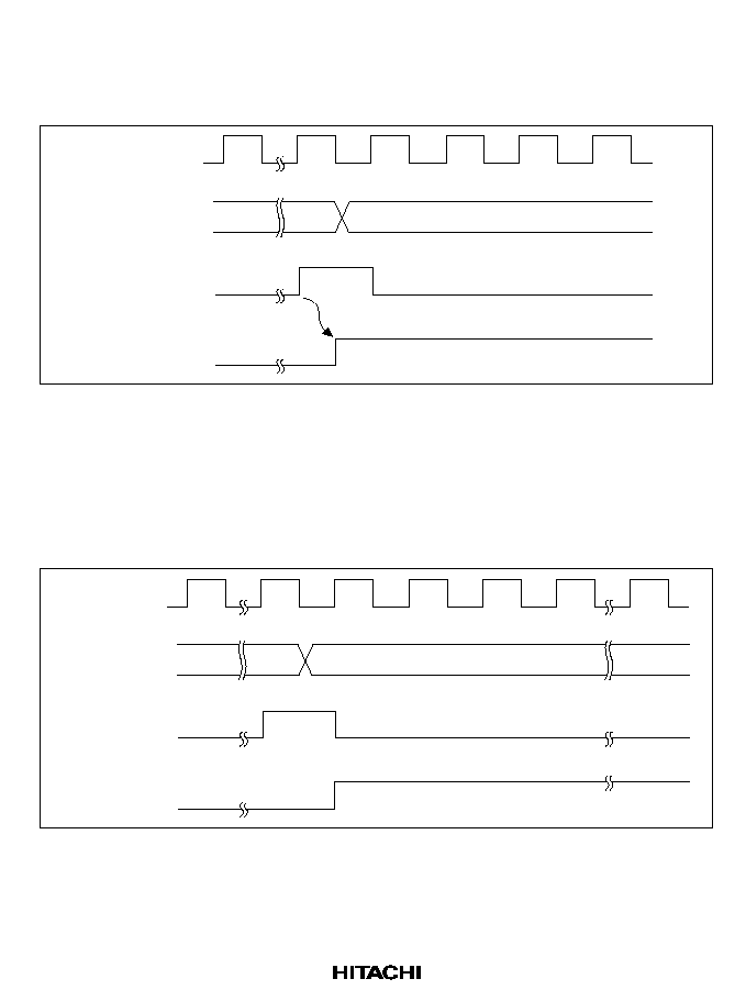
329
12.3.4
Timing of Overflow Flag (OVF) Setting
In interval timer mode, when WTCNT overflows, the OVF flag in WTCSR is set to 1 and an
interval timer interrupt (ITI) is requested (figure 12.6).
WTCNT
H'FF
H'00
Overflow signal
(internal signal)
OVF
Figure 12.6 Timing of OVF Setting
12.3.5
Timing of Watchdog Timer Overflow Flag (WOVF) Setting
When WTCNT overflows the WOVF flag in RSTCSR is set to 1 and a
WDTOVF signal is output.
When the RSTE bit is set to 1, WTCNT overflow enables an internal reset signal to be generated
for the entire chip (figure 12.7).
WTCNT
H'FF
H'00
Overflow signal
(internal signal)
WOVF
Figure 12.7 Timing of WOVF Setting
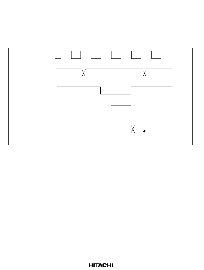
330
12.4
Usage Notes
12.4.1
Contention between WTCNT Write and Increment
If a timer counter clock pulse is generated during the T3 state of a write cycle to WTCNT, the
write takes priority and the timer counter is not incremented (figure 12.8).
WTCNT address
Address
Internal write
signal
WTCNT input
clock
WTCNT
Counter write data
N
M
Figure 12.8 Contention between WTCNT Write and Increment
12.4.2
Changing CKS2 to CKS0 Bit Values
If the values of bits CKS2 to CKS0 are altered while the WDT is running, the count may
increment incorrectly. Always stop the watchdog timer (by clearing the TME bit to 0) before
changing the values of bits CKS2 to CKS0.
12.4.3
Switching between Watchdog Timer and Interval Timer Mode
To prevent incorrect operation, always stop the watchdog timer (by clearing the TME bit to 0)
before switching between interval timer mode and watchdog timer mode.
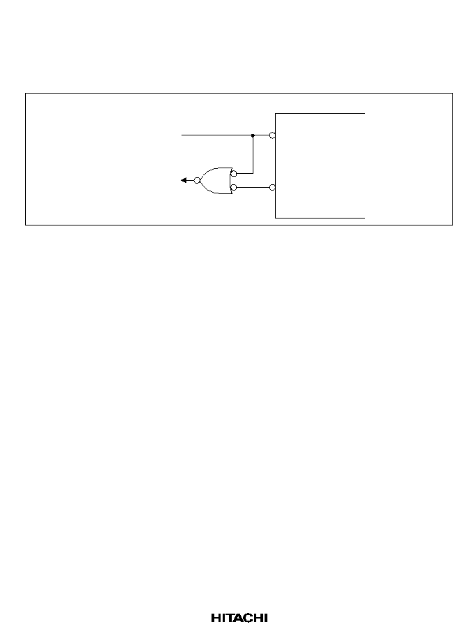
331
12.4.4
System Reset with
WDTOVF
If a
WDTOVF signal is input to the RES pin, the device cannot initialize correctly. Avoid logical
input of the
WDTOVF output signal to the RES input pin. To reset the entire system with the
WDTOVF signal, use the circuit shown in figure 12.9.
Reset input
Reset signal to
entire system
SH microprocessor
RES
WDTOVF
Figure 12.9 Example of Circuit for System Reset with
WDTOVF Signal
12.4.5
Internal Reset in Watchdog Timer Mode
If the RSTE bit is cleared to 0 in watchdog timer mode, the chip will not reset internally when a
WTCNT overflow occurs, but WTCNT and WTCSR in the WDT will reset.

332

333
Section 13 Serial Communication Interface
13.1
Overview
The SH7604 has a serial communication interface (SCI) that supports both asynchronous and
clocked synchronous serial communication. It also has a multiprocessor communication function
for serial communication among two or more processors.
13.1.1
Features
Selection of asynchronous or clock synchronous as the serial communication mode
·
Asynchronous mode:
Serial data communication is synchronized by the start-stop method in character units. The
SCI can communicate with a universal asynchronous receiver/transmitter (UART), an
asynchronous communication interface adapter (ACIA), or any other chip that employs
standard asynchronous serial communication. It can also communicate with two or more
other processors using the multiprocessor communication function. There are twelve
selectable serial data communication formats.
Data length: seven or eight bits
Stop bit length: one or two bits
Parity: even, odd, or none
Multiprocessor bit: one or none
Receive error detection: parity, overrun, and framing errors
·
Clocked synchronous mode:
Serial data communication is synchronized with a clock signal. The SCI can communicate
with other chips having a clocked synchronous communication function. There is one serial
data communication format.
Data length: eight bits
Receive error detection: overrun errors
·
Full duplex communication. The transmitting and receiving sections are independent, so the
SCI can transmit and receive simultaneously. Both sections use double buffering, so
continuous data transfer is possible in both the transmit and receive directions.
·
Built-in baud rate generator with selectable bit rates
·
Internal or external transmit/receive clock source. Baud rate generator (internal) or SCK pin
(external)
·
Four types of interrupts. Transmit-data-empty, transmit-end, receive-data-full, and receive-
error interrupts are requested independently. The transmit-data-empty and receive-data-full
interrupts can start the direct memory access controller (DMAC) to transfer data.
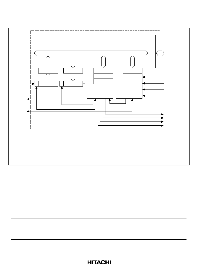
334
13.1.2
Block Diagram
Figure 13.1 shows a block diagram of the SCI.
RxD
TxD
SCK
SCI
BRR
SSR
SCR
TDR
TSR
RDR
RSR
SMR
Parity generation
Parity check
Clock
External clock
Module data bus
Internal
data bus
/4
/16
/64
/256
TEI
TXI
RXI
ERI
Bus interface
Baud rate
generator
Transmit/
receive
control
RSR: Receive shift register
SMR: Serial mode register
RDR: Receive data register
SCR: Serial control register
TSR: Transmit shift register
SSR: Serial status register
TDR: Transmit data register
BRR: Bit rate register
Figure 13.1 SCI Block Diagram
13.1.3
Pin Configuration
Table 13.1 summarizes the SCI pins.
Table 13.1
SCI Pins
Pin Name
Abbreviation Input/Output
Function
Serial clock pin
SCK
Input/output
Clock input/output
Receive data pin
RxD
Input
Receive data input
Transmit data pin
TxD
Output
Transmit data output
335
13.1.4
Register Configuration
Table 13.2 summarizes the SCI internal registers. These registers select the communication mode
(asynchronous or clock synchronous), specify the data format and bit rate, and control the
transmitter and receiver sections.
Table 13.2
Registers
Name
Abbreviation R/W
Initial Value Address
Access size
Serial mode register
SMR
R/W
H'00
H'FFFFFE00 8
Bit rate register
BRR
R/W
H'FF
H'FFFFFE01 8
Serial control register
SCR
R/W
H'00
H'FFFFFE02 8
Transmit data register
TDR
R/W
H'FF
H'FFFFFE03 8
Serial status register
SSR
R/(W)
*
H'84
H'FFFFFE04 8
Receive data register
RDR
R
H'00
H'FFFFFE05 8
Note:
The only value that can be written is a 0 to clear the flags.
13.2
Register Descriptions
13.2.1
Receive Shift Register (RSR)
The receive shift register (RSR) receives serial data. Data input at the RxD pin is loaded into RSR
in the order received, LSB (bit 0) first, converting the data to parallel form. When one byte has
been received, it is automatically transferred to RDR. The CPU cannot read or write to RSR
directly.
Bit:
7
6
5
4
3
2
1
0
Bit name:
R/W:
--
--
--
--
--
--
--
--
13.2.2
Receive Data Register (RDR)
The receive data register (RDR) stores serial receive data. The SCI completes the reception of one
byte of serial data by moving the received data from the receive shift register (RSR) into RDR for
storage. RSR is then ready to receive the next data. This double buffering allows the SCI to
receive data continuously.
The CPU can read but not write to RDR. RDR is initialized to H'00 by a reset and in standby and
module standby mode.

336
Bit:
7
6
5
4
3
2
1
0
Bit name:
Initial value:
0
0
0
0
0
0
0
0
R/W:
R
R
R
R
R
R
R
R
13.2.3
Transmit Shift Register (TSR)
The transmit shift register (TSR) transmits serial data. The SCI loads transmit data from the
transmit data register (TDR) into TSR, then transmits the data serially from the TxD pin, LSB (bit
0) first. After transmitting one data byte, the SCI automatically loads the next transmit data from
TDR into TSR and starts transmitting again. If the TDRE bit in SSR is 1, however, the SCI does
not load the TDR contents into TSR. The CPU cannot read or write to TSR directly.
Bit:
7
6
5
4
3
2
1
0
Bit name:
R/W:
--
--
--
--
--
--
--
--
13.2.4
Transmit Data Register (TDR)
The transmit data register (TDR) is an 8-bit register that stores data for serial transmission. When
the SCI detects that the transmit shift register (TSR) is empty, it moves transmit data written in
TDR into TSR and starts serial transmission. Continuous serial transmission is possible by writing
the next transmit data in TDR during serial transmission from TSR.
The CPU can always read and write to TDR. TDR is initialized to H'FF by a reset and in standby
and module standby mode.
Bit:
7
6
5
4
3
2
1
0
Bit name:
Initial value:
1
1
1
1
1
1
1
1
R/W:
R/W
R/W
R/W
R/W
R/W
R/W
R/W
R/W
13.2.5
Serial Mode Register (SMR)
The serial mode register (SMR) is an 8-bit register that specifies the SCI serial communication
format and selects the clock source for the baud rate generator.
The CPU can always read and write to SMR. SMR is initialized to H'00 by a reset and in standby
and module standby mode.

337
Bit:
7
6
5
4
3
2
1
0
Bit name:
C /
A
CHR
PE
O/
E
STOP
MP
CKS1
CKS0
Initial value:
0
0
0
0
0
0
0
0
R/W:
R/W
R/W
R/W
R/W
R/W
R/W
R/W
R/W
·
Bit 7--Communication Mode (C/
A): Selects whether the SCI operates in asynchronous or
clocked synchronous mode.
Bit 7: C/A
Description
0
Asynchronous mode
(Initial value)
1
Clocked synchronous mode
·
Bit 6--Character Length (CHR): Selects 7-bit or 8-bit data in asynchronous mode. In clocked
synchronous mode, the data length is always eight bits, regardless of the CHR setting.
Bit 6: CHR
Description
0
8-bit data
(Initial value)
1
7-bit data. (When 7-bit data is selected, the MSB (bit 7) of the transmit
data register is not transmitted.)
·
Bit 5--Parity Enable (PE): Selects whether to add a parity bit to transmit data and to check the
parity of receive data, in asynchronous mode. In clocked synchronous mode, a parity bit is
neither added nor checked, regardless of the PE setting.
Bit 5: PE
Description
0
Parity bit not added or checked
(Initial value)
1
Parity bit added and checked. When PE is set to 1, an even or odd
parity bit is added to transmit data, depending on the parity mode (O/
E
)
setting. Receive data parity is checked according to the even/odd (O/
E
)
mode setting.
·
Bit 4--Parity Mode (O/
E): Selects even or odd parity when parity bits are added and checked.
The O/
E setting is used only in asynchronous mode and only when the parity enable bit (PE) is
set to 1 to enable parity addition and checking. The O/
E setting is ignored in clocked
synchronous mode, and in asynchronous mode when parity addition and checking is disabled.

338
Bit 4: O/
E
Description
0
Even parity
(Initial value)
If even parity is selected, the parity bit is added to transmit data to make
an even number of 1s in the transmitted character and parity bit
combined. Receive data is checked to see if it has an even number of
1s in the received character and parity bit combined.
1
Odd parity
If odd parity is selected, the parity bit is added to transmit data to make
an odd number of 1s in the transmitted character and parity bit
combined. Receive data is checked to see if it has an odd number of 1s
in the received character and parity bit combined.
·
Bit 3--Stop Bit Length (STOP): Selects one or two bits as the stop bit length in asynchronous
mode. This setting is used only in asynchronous mode. It is ignored in clocked synchronous
mode because no stop bits are added.
·
In receiving, only the first stop bit is checked, regardless of the STOP bit setting. If the second
stop bit is 1, it is treated as a stop bit, but if the second stop bit is 0, it is treated as the start bit
of the next incoming character.
Bit 3: STOP
Description
0
One stop bit
(Initial value)
In transmitting, a single 1-bit is added at the end of each transmitted
character
1
Two stop bits
In transmitting, two 1-bits are added at the end of each transmitted
character
·
Bit 2--Multiprocessor Mode (MP): Selects multiprocessor format. When multiprocessor
format is selected, settings of the parity enable (PE) and parity mode (O/
E) bits are ignored.
The MP bit setting is used only in asynchronous mode; it is ignored in clocked synchronous
mode. For the multiprocessor communication function, see section 13.3.3, Multiprocessor
Communication.
Bit 2: MP
Description
0
Multiprocessor function disabled
(Initial value)
1
Multiprocessor format selected
339
·
Bits 1 and 0--Clock Select 1 and 0 (CKS1 and CKS0): These bits select the internal clock
source of the built-in baud rate generator. Four clock sources are available.
/4,
/16,
/64 and
/256. For further information on the clock source, bit rate register settings, and baud rate, see
section 13.2.8, Bit Rate Register.
Bit 1: CKS1
Bit 0: CKS0
Description
0
0
/4
(Initial value)
1
/16
1
0
/64
1
/256
13.2.6
Serial Control Register (SCR)
The serial control register (SCR) operates the SCI transmitter/receiver, selects the serial clock
output in asynchronous mode, enables/disables interrupts, and selects the transmit/receive clock
source. The CPU can always read and write to SCR. SCR is initialized to H'00 by a reset and in
standby and module standby modes.
Bit:
7
6
5
4
3
2
1
0
Bit name:
TIE
RIE
TE
RE
MPIE
TEIE
CKE1
CKE0
Initial value:
0
0
0
0
0
0
0
0
R/W:
R/W
R/W
R/W
R/W
R/W
R/W
R/W
R/W
·
Bit 7--Transmit Interrupt Enable (TIE): Enables or disables the transmit-data-empty interrupt
(TXI) requested when the transmit data register empty bit (TDRE) in the serial status register
(SSR) is set to 1 due to transfer of serial transmit data from TDR to TSR.
Bit 7: TIE
Description
0
Transmit-data-empty interrupt request (TXI) is disabled
(Initial value)
The TXI interrupt request can be cleared by reading TDRE after it has
been set to 1, then clearing TDRE to 0, or by clearing TIE to 0.
1
Transmit-data-empty interrupt request (TXI) is enabled
·
Bit 6--Receive Interrupt Enable (RIE): Enables or disables the receive-data-full interrupt
(RXI) requested when the receive data register full bit (RDRF) in the serial status register
(SSR) is set to 1 due to transfer of serial receive data from RSR to RDR. It also enables or
disables receive-error interrupt (ERI) requests.

340
Bit 6: RIE
Description
0
Receive-data-full interrupt (RXI) and receive-error interrupt (ERI)
requests are disabled
(Initial value)
RXI and ERI interrupt requests can be cleared by reading the RDRF
flag or error flag (FER, PER, or ORER) after it has been set to 1, then
clearing the flag to 0, or by clearing RIE to 0.
1
Receive-data-full interrupt (RXI) and receive-error interrupt (ERI)
requests are enabled
·
Bit 5--Transmit Enable (TE): Enables or disables the SCI serial transmitter.
Bit 5: TE
Description
0
Transmitter disabled
(Initial value)
The transmit data register empty bit (TDRE) in the serial status register
(SSR) is locked at 1
1
Transmitter enabled
Serial transmission starts when the transmit data register empty (TDRE)
bit in the serial status register (SSR) is cleared to 0 after writing of
transmit data into TDR. Select the transmit format in SMR before setting
TE to 1.
·
Bit 4--Receive Enable (RE): Enables or disables the SCI serial receiver.
Bit 4: RE
Description
0
Receiver disabled
(Initial value)
Clearing RE to 0 does not affect the receive flags (RDRF, FER, PER,
ORER). These flags retain their previous values.
1
Receiver enabled
Serial reception starts when a start bit is detected in asynchronous
mode, or synchronous clock input is detected in clocked synchronous
mode. Select the receive format in SMR before setting RE to 1.
·
Bit 3--Multiprocessor Interrupt Enable (MPIE): Enables or disables multiprocessor interrupts.
The MPIE setting is used only in asynchronous mode, and only if the multiprocessor mode bit
(MP) in the serial mode register (SMR) is set to 1 during reception. The MPIE setting is
ignored in clocked synchronous mode or when the MP bit is cleared to 0.

341
Bit 3: MPIE
Description
0
Multiprocessor interrupts are disabled (normal receive operation)
(Initial value)
MPE is cleared to 0 when MPIE is cleared to 0, or the multiprocessor bit
(MPB) is set to 1 in receive data.
1
Multiprocessor interrupts are enabled
Receive-data-full interrupt requests (RXI), receive-error interrupt
requests (ERI), and setting of the RDRF, FER, and ORER status flags
in the serial status register (SSR) are disabled until the multiprocessor
bit is set to 1.
The SCI does not transfer receive data from RSR to RDR, does not
detect receive errors, and does not set the RDRF, FER, and ORER
flags in the serial status register (SSR). When it receives data that
includes MPB = 1, MPB is set to 1 in SSR, and the SCI automatically
clears MPIE to 0, generates RXI and ERI interrupts (if the TIE and RIE
bits in SCR are set to 1), and enables the FER and ORER bits to be set.
·
Bit 2--Transmit-End Iinterrupt Enable (TEIE): Enables or disables the transmit-end interrupt
(TEI) requested if TDR does not contain new transmit data when the MSB is transmitted.
Bit 2: TEIE
Description
0
Transmit-end interrupt (TEI) requests are disabled*
(Initial value)
1
Transmit-end interrupt (TEI) requests are enabled*
Note:
The TEI request can be cleared by reading the TDRE bit in the serial status register (SSR)
after it has been set to 1, then clearing TDRE to 0; by clearing the transmit end (TEND) bit
to 0; or by clearing the TEIE bit to 0.
·
Bits 1 and 0--Clock Enable 1 and 0 (CKE1 and CKE0): These bits select the SCI clock source
and enable or disable clock output from the SCK pin. Depending on the combination of CKE1
and CKE0, the SCK pin can be used for general-purpose input/output, serial clock output, or
serial clock input.
The CKE0 setting is valid only in asynchronous mode, and only when the SCI is internally
clocked (CKE1 = 0). The CKE0 setting is ignored in clocked synchronous mode, or when an
external clock source is selected (CKE1 = 1). Select the SCI operating mode in the serial mode
register (SMR) before setting CKE1 and CKE0. For further details on selection of the SCI
clock source, see table 13.9 in section 13.3, Operation.

342
Bit 1:
CKE1
Bit 0:
CKE0 Description
0
0
Asynchronous mode
Internal clock, SCK pin used for input pin (input signal
is ignored or output pin output level is undefined)
*1
Clocked synchronous mode
Internal clock, SCK pin used for synchronous clock
output*
1
0
1
Asynchronous mode
Internal clock, SCK pin used for clock output*
2
Clocked synchronous mode
Internal clock, SCK pin used for synchronous clock
output
1
0
Asynchronous mode
External clock, SCK pin used for clock input*
3
Clocked synchronous mode
External clock, SCK pin used for synchronous clock
input
1
1
Asynchronous mode
External clock, SCK pin used for clock input*
3
Clocked synchronous mode
External clock, SCK pin used for synchronous clock
input
Notes: 1. Initial value
2. The output clock frequency is the same as the bit rate.
3. The input clock frequency is 16 times the bit rate.
13.2.7
Serial Status Register (SSR)
The serial status register (SSR) is an 8-bit register containing multiprocessor bit values, and status
flags that indicate the SCI operating status.
The CPU can always read and write to SSR, but cannot write 1 in the status flags (TDRE, RDRF,
ORER, PER, and FER). These flags can be cleared to 0 only if they have first been read (after
being set to 1). Bits 2 (TEND) and 1 (MPB) are read-only bits that cannot be written. SSR is
initialized to H'84 by a reset and in standby and module standby mode.
Bit:
7
6
5
4
3
2
1
0
Bit name:
TDRE
RDRF
ORER
FER
PER
TEND
MPB
MPBT
Initial value:
1
0
0
0
0
1
0
0
R/W:
R/(W)*
R/(W)*
R/(W)*
R/(W)*
R/(W)*
R
R
R/W
Note:
The only value that can be written is a 0 to clear the flag.
·
Bit 7--Transmit Data Register Empty (TDRE): Indicates that the SCI has loaded transmit data
from TDR into TSR and new serial transmit data can be written in TDR.

343
Bit 7: TDRE
Description
0
TDR contains valid transmit data
TDRE is cleared to 0 when software reads TDRE after it has been set to 1, then
writes 0 in TDRE, or the DMAC writes data in TDR.
1
TDR does not contain valid transmit data
(Initial value)
TDRE is set to 1 when the chip is reset or enters standby mode, the TE bit in the
serial control register (SCR) is cleared to 0, or TDR contents are loaded into
TSR, so new data can be written in TDR.
·
Bit 6--Receive Data Register Full (RDRF): Indicates that RDR contains received data.
Bit 6: RDRF
Description
0
RDR does not contain valid receive data
(Initial value)
RDRF is cleared to 0 when the chip is reset or enters standby mode, software
reads RDRF after it has been set to 1, then writes 0 in RDRF, or the DMAC
reads data from RDR.
1
RDR contains valid received data
RDRF is set to 1 when serial data is received normally and transferred from RSR
to RDR.
Note:
RDR and RDRF are not affected by detection of receive errors or by clearing of the RE bit
to 0 in the serial control register. They retain their previous contents. If RDRF is still set to 1
when reception of the next data ends, an overrun error (ORER) occurs and the received
data is lost.
·
Bit 5--Overrun Error (ORER): Indicates that data reception ended abnormally due to an
overrun error.
Bit 5: ORER
Description
0
Receiving is in progress or has ended normally
*1
(Initial value)
ORER is cleared to 0 when the chip is reset or enters standby mode, or software
reads ORER after it has been set to 1, then writes 0 in ORER.
1
A receive overrun error occurred
*2
ORER is set to 1 if reception of the next serial data ends when RDRF is set to 1.
Notes: 1. Clearing the RE bit to 0 in the serial control register does not affect the ORER bit, which
retains its previous value.
2. RDR continues to hold the data received before the overrun error, so subsequent
receive data is lost. Serial receiving cannot continue while ORER is set to 1. In clocked
synchronous mode, serial transmitting is disabled.

344
·
Bit 4--Framing Error (FER): Indicates that data reception ended abnormally due to a framing
error in asynchronous mode.
Bit 4: FER
Description
0
Receiving is in progress or has ended normally
(Initial value)
Clearing the RE bit to 0 in the serial control register does not affect the FER bit,
which retains its previous value.
FER is cleared to 0 when the chip is reset or enters standby mode, or software
reads FER after it has been set to 1, then writes 0 in FER.
1
A receive framing error occurred
When the stop bit length is two bits, only the first bit is checked. The second stop
bit is not checked. When a framing error occurs, the SCI transfers the receive
data into RDR but does not set RDRF. Serial receiving cannot continue while
FER is set to 1. In clocked synchronous mode, serial transmitting is also
disabled.
FER is set to 1 if the stop bit at the end of receive data is checked and found to
be 0.
·
Bit 3--Parity Error (PER): Indicates that data reception (with parity) ended abnormally due to
a parity error in asynchronous mode.
Bit 3: PER
Description
0
Receiving is in progress or has ended normally
(Initial value)
Clearing the RE bit to 0 in the serial control register does not affect the PER bit,
which retains its previous value.
PER is cleared to 0 when the chip is reset or enters standby mode, or software
reads PER after it has been set to 1, then writes 0 in PER.
1
A receive parity error occurred
When a parity error occurs, the SCI transfers the receive data into RDR but does
not RDRF. Serial receiving cannot continue while PER is set to 1. In clocked
synchronous mode, serial transmitting is also disabled.
PER is set to 1 if the number of 1s in receive data, including the parity bit, does
not match the even or odd parity setting of the parity mode bit (O/
E
) in the serial
mode register (SMR).

345
·
Bit 2--Transmit End (TEND): Indicates that when the last bit of a serial character was
transmitted, TDR did not contain valid data, so transmission has ended. TEND is a read-only
bit and cannot be written.
Bit 2: TEND
Description
0
Transmission is in progress
TEND is cleared to 0 when software reads TDRE after it has been set to 1, then
writes 0 in TDRE, or the DMAC writes data in TDR.
1
End of transmission
(Initial value)
TEND is set to 1 when the chip is reset or enters standby mode, TE is cleared to
0 in the serial control register (SCR), or TDRE is 1 when the last bit of a one-byte
serial character is transmitted.
·
Bit 1--Multiprocessor Bit (MPB): Stores the value of the multiprocessor bit in receive data
when a multiprocessor format is selected for receiving in asynchronous mode. MPB is a read-
only bit and cannot be written.
Bit 1: MPB
Description
0
Multiprocessor bit value in receive data is 0
(Initial value)
If RE is cleared to 0 when a multiprocessor format is selected, MPB retains its
previous value.
1
Multiprocessor bit value in receive data is 1
·
Bit 0--Multiprocessor Bit Transfer (MPBT): Stores the value of the multiprocessor bit added
to transmit data when a multiprocessor format is selected for transmitting in asynchronous
mode. The MPBT setting is ignored in clocked synchronous mode, when a multiprocessor
format is not selected, or when the SCI is not transmitting.
Bit 0: MPBT
Description
0
Multiprocessor bit value in transmit data is 0
(Initial value)
1
Multiprocessor bit value in transmit data is 1

346
13.2.8
Bit Rate Register (BRR)
The bit rate register (BRR) is an 8-bit register that, together with the baud rate generator clock
source selected by the CKS1 and CKS0 bits in the serial mode register (SMR), determines the
serial transmit/receive bit rate.
The CPU can always read and write to BRR. BRR is initialized to H'FF by a reset and in standby
mode.
Bit:
7
6
5
4
3
2
1
0
Bit name:
Initial value:
1
1
1
1
1
1
1
1
R/W:
R/W
R/W
R/W
R/W
R/W
R/W
R/W
R/W
Table 13.3 shows examples of BRR settings in asynchronous mode; table 13.4 shows examples of
BBR settings in clocked synchronous mode.

347
Table 13.3
Bit Rates and BRR Settings in Asynchronous Mode
(MHz)
4
4.9152
8
9.8304
Bit Rate
(bits/s)
n
N
Error
(%)
n
N
Error
(%)
n
N
Error
(%)
n
N
Error
(%)
110
1
70
0.03
1
86
0.31
1
141
0.03
1
174
0.26
150
0
207
0.16
0
255
0.00
1
103
0.16
1
127
0.00
300
0
103
0.16
0
127
0.00
0
207
0.16
0
255
0.00
600
0
51
0.16
0
63
0.00
0
103
0.16
0
127
0.00
1200
0
25
0.16
0
31
0.00
0
51
0.16
0
63
0.00
2400
0
12
0.16
0
15
0.00
0
25
0.16
0
31
0.00
4800
--
--
--
0
7
0.00
0
12
0.16
0
15
0.00
9600
--
--
--
0
3
0.00
--
--
--
0
7
0.00
19200
--
--
--
0
1
0.00
--
--
--
0
3
0.00
31250
0
0
0.00
--
--
--
0
1
0.00
--
--
--
38400
--
--
--
0
0
0.00
--
--
--
0
1
0.00
(MHz)
12
14.7456
16
19.6608
Bit Rate
(bits/s)
n
N
Error
(%)
n
N
Error
(%)
n
N
Error
(%)
n
N
Error
(%)
110
1
212
0.03
2
64
0.70
2
70
0.03
2
86
0.31
150
1
155
0.16
1
191
0.00
1
207
0.16
1
255
0.00
300
1
77
0.16
1
95
0.00
1
103
0.16
1
127
0.00
600
0
155
0.16
0
191
0.00
0
207
0.16
0
255
0.00
1200
0
77
0.16
0
95
0.00
0
103
0.16
0
127
0.00
2400
0
38
0.16
0
47
0.00
0
51
0.16
0
63
0.00
4800
0
19
2.34
0
23
0.00
0
25
0.16
0
31
0.00
9600
0
9
2.34
0
11
0.00
0
12
0.16
0
15
0.00
19200
0
4
2.34
0
5
0.00
--
--
--
0
7
0.00
31250
0
2
0.00
--
--
--
0
3
0.00
0
4
1.70
38400
--
--
--
0
2
0.00
--
--
--
0
3
0.00

348
Table 13.3
Bit Rates and BRR Settings in Asynchronous Mode (cont)
(MHz)
20
24
24.576
28.7
Bit Rate
(bits/s)
n
N
Error
(%)
n
N
Error
(%)
n
N
Error
(%)
n
N
Error
(%)
110
2
88
0.25
2
106
0.44
2
108
0.08
2
126
0.31
150
2
64
0.16
2
77
0.16
2
79
0.00
2
92
0.46
300
1
129
0.16
1
155
0.16
1
159
0.00
1
186
-0.08
600
1
64
0.16
1
77
0.16
1
79
0.00
1
92
0.46
1200
0
129
0.16
0
155
0.16
0
159
0.00
0
186
-0.08
2400
0
64
0.16
0
77
0.16
0
79
0.00
0
92
0.46
4800
0
32
1.36
0
38
0.16
0
39
0.00
0
46
-0.61
9600
0
15
1.73
0
19
2.34
0
19
0.00
0
22
1.55
19200
0
7
1.73
0
9
2.34
0
9
0.00
0
11
-2.68
31250
0
4
0.00
0
5
0.00
0
5
2.40
0
6
2.50
38400
0
3
1.73
0
4
2.34
0
4
0.00
0
5
-2.68

349
Table 13.4
Bit Rates and BRR Settings in Clocked Synchronous Mode
(MHz)
Bit Rate
4
8
16
28.7
(bits/s)
n
N
n
N
n
N
n
N
110
2
141
3
70
3
141
3
254
250
1
249
2
124
2
249
3
111
500
1
124
1
249
2
124
2
223
1k
0
249
1
124
1
249
2
111
2.5k
0
99
0
199
1
99
1
178
5k
0
49
0
99
0
199
1
89
10k
0
24
0
49
0
99
0
178
25k
0
9
0
19
0
39
0
71
50k
0
4
0
9
0
19
0
35
100k
--
--
0
4
0
9
0
17
250k
0
0*
0
1
0
3
--
--
500k
0
0*
0
1
--
--
1M
0
0*
--
--
Note:
Settings with an error of 1% or less are recommended.
Explanation of symbols:
Blank:
No setting possible
--:
Setting possible, but error occurs
*:
Continuous transmission/reception not possible
The BRR setting is calculated as follows:
Asynchronous mode:
N =
256
×
2
2n 1
×
B
×
10
6
1
Clocked synchronous mode:
N =
32
×
2
2n 1
×
B
×
10
6
1
B: Bit rate (bit/s)
N: BRR setting for baud rate generator (0
N
255)
f:
Operating frequency (MHz)
n: Baud rate generator clock source (n = 0, 1, 2, 3) (For the clock sources and values of n,
see table 13.6.)

350
Table 13.5
SMR Settings
SMR Settings
n
Clock Source
CKS1
CKS0
0
/4
0
0
1
/16
0
1
2
/164
1
0
3
/256
1
1
The bit rate error for asynchronous mode is given by the following equation:
Error (%) =
×
10
6
(N + 1)
×
B
×
256
×
2
2n 1
1
×
100
Table 13.6 shows the maximum bit rates in asynchronous mode when the baud rate generator is
being used. Tables 13.7 and 13.8 show the maximum rates for external clock input.
Table 13.6
Maximum Bit Rates for Various Frequencies with Baud Rate Generator
(Asynchronous Mode)
Settings
(MHz)
Maximum Bit Rate (bits/s)
n
N
4
31250
0
0
4.9152
38400
0
0
8
62500
0
0
9.8304
76800
0
0
12
93750
0
0
14.7456
115200
0
0
16
125000
0
0
19.6608
153600
0
0
20
156250
0
0
24
187500
0
0
24.576
192000
0
0
28.7
224218
0
0

351
Table 13.7
Maximum Bit Rates with External Clock Input (Asynchronous Mode)
(MHz)
External Input Clock (MHz)
Maximum Bit Rate (bits/s)
4
0.2500
15625
4.9152
0.3072
19200
8
0.5000
31250
9.8304
0.6144
38400
12
0.7500
46875
14.7456
0.9216
57600
16
1.0000
62500
19.6608
1.2288
76800
20
1.2500
78125
24
1.5000
93750
24.576
1.5360
96000
28.7
1.79375
112109
Table 13.8
Maximum Bit Rates with External Clock Input (Clocked Synchronous Mode)
(MHz)
External Input Clock (MHz)
Maximum Bit Rate (bits/s)
8
0.3333
333333.3
16
0.6667
666666.7
24
1.0000
1000000.0
28.7
1.1958
1195833.3

352
13.3
Operation
13.3.1
Overview
For serial communication, the SCI has an asynchronous mode in which characters are
synchronized individually, and a clocked synchronous mode in which communication is
synchronized with clock pulses. Asynchronous/clocked synchronous mode and the communication
format are selected in the serial mode register (SMR), as shown in table 13.9. The SCI clock
source is selected by the C/
A bit in the serial mode register (SMR) and the CKE1 and CKE0 bits
in the serial control register (SCR), as shown in table 13.10.
Asynchronous Mode:
·
Data length is selectable. seven or eight bits.
·
Parity and multiprocessor bits are selectable, as is the stop bit length (one or two bits). The
preceding selections constitute the communication format and character length.
·
In receiving, it is possible to detect framing errors, parity errors, overrun errors, and the break
state.
·
An internal or external clock can be selected as the SCI clock source.
When an internal clock is selected, the SCI operates using the built-in baud rate generator,
and can output a serial clock signal with a frequency matching the bit rate.
When an external clock is selected, the external clock input must have a frequency 16 times
the bit rate. (The built-in baud rate generator is not used.)
Clocked Synchronous Mode:
·
The communication format has a fixed eight-bit data length.
·
In receiving, it is possible to detect overrun errors.
·
An internal or external clock can be selected as the SCI clock source.
When an internal clock is selected, the SCI operates using the built-in baud rate generator,
and outputs a synchronous clock signal to external devices.
When an external clock is selected, the SCI operates on the input synchronous clock. The
built-in baud rate generator is not used.

353
Table 13.9
Serial Mode Register Settings and SCI Communication Formats
SMR Settings
SCI Communication Format
Mode
Bit 7
C/A
Bit 6
CHR
Bit 5
PE
Bit 2
MP
Bit 3
STOP
Data
Length
Parity
Bit
Multipro-
cessor Bit
Stop Bit
Length
Asynchronous
0
0
0
0
0
8-bit
Not set
Not set
1 bit
1
2 bits
1
0
Set
1 bit
1
2 bits
1
0
0
7-bit
Not set
1 bit
1
2 bits
1
0
Set
1 bit
1
2 bits
Asynchronous
0
0
*
1
0
8-bit
Not set
Set
1 bit
(multiprocessor
*
1
2 bits
format)
1
*
0
7-bit
1 bit
*
1
2 bits
Clocked
synchronous
1
*
*
*
*
8-bit
Not set
Not set
None
Note:
Asterisks (*) in the table indicate don't care bits.
Table 13.10
SMR and SCR Settings and SCI Clock Source Selection
SMR
SCR Settings
SCI Transmit/Receive Clock
Mode
Bit 7
C/
A
Bit 1
CKE1
Bit 0
CKE0
Clock Source
SCK Pin Function
Asynchronous
0
0
0
Internal
SCI does not use the SCK pin
1
Outputs a clock with frequency
matching the bit rate
1
0
External
Inputs a clock with frequency 16 times
the bit rate
1
Clocked synch- 1
0
0
Internal
Outputs the synchronous clock
ronous
1
1
0
External
Inputs the synchronous clock
1
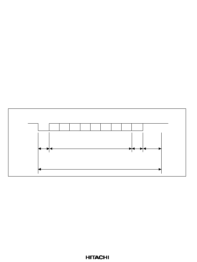
354
13.3.2
Operation in Asynchronous Mode
In asynchronous mode, each transmitted or received character begins with a start bit and ends with
a stop bit. Serial communication is synchronized one character at a time.
The transmitting and receiving sections of the SCI are independent, so full duplex communication
is possible. The transmitter and receiver are both double buffered, so data can be written and read
while transmitting and receiving are in progress, enabling continuous transmitting and receiving.
Figure 13.2 shows the general format of asynchronous serial communication. In asynchronous
serial communication, the communication line is normally held in the mark (high) state. The SCI
monitors the line and starts serial communication when the line goes to the space (low) state,
indicating a start bit. One serial character consists of a start bit (low), data (LSB first), parity bit
(high or low), and stop bit (high), in that order.
When receiving in asynchronous mode, the SCI synchronizes on the falling edge of the start bit.
The SCI samples each data bit on the eighth pulse of a clock with a frequency 16 times the bit rate.
Receive data is latched at the center of each bit.
0
D
0
D
1
D
2
D
3
D
4
D
5
D
6
D
7
1
1
0/1
1
1
(LSB)
(MSB)
Serial
data
State
bit
1 bit
Transmit/receive data
7 or 8 bits
One unit of communication data (character or frame)
Idle (mark) state
Parity
bit
Stop
bit
1 or
no bit
1 or
2 bits
Figure 13.2 Example of Data Format in Asynchronous Communication
(8-Bit Data with Parity and Two Stop Bits)
355
Transmit/Receive Formats. Table 13.11 shows the 12 communication formats that can be
selected in asynchronous mode. The format is selected by settings in the serial mode register
(SMR).
Table 13.11
Serial Communication Formats (Asynchronous Mode)
SMR Bits
Serial Transmit/Receive Format and Frame Length
CHR PE
MP
STOP
1
2
3
4
5
6
7
8
9
10
11
12
0
0
0
0
START
8-bit data
STOP
0
0
0
1
START
8-bit data
STOP STOP
0
1
0
0
START
8-bit data
P
STOP
0
1
0
1
START
8-bit data
P
STOP STOP
1
0
0
0
START
7-bit data
STOP
1
0
0
1
START
7-bit data
STOP STOP
1
1
0
0
START
7-bit data
P
STOP
1
1
0
1
START
7-bit data
P
STOP STOP
0
--
1
0
START
8-bit data
MPB
STOP
0
--
1
1
START
8-bit data
MPB
STOP STOP
1
--
1
0
START
7-bit data
MPB
STOP
1
--
1
1
START
7-bit data
MPB
STOP STOP
--: Don't care bits.
START: Start bit
STOP: Stop bit
P: Parity bit
MPB: Multiprocessor bit
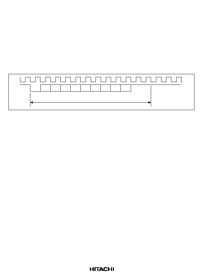
356
Clock: An internal clock generated by the built-in baud rate generator or an external clock input
from the SCK pin can be selected as the SCI transmit/receive clock. The clock source is selected
by the C/
A bit in the serial mode register (SMR) and bits CKE1 and CKE0 in the serial control
register (SCR) (table 13.9).
When an external clock is input at the SCK pin, it must have a frequency equal to 16 times the
desired bit rate.
When the SCI operates on an internal clock, it can output a clock signal at the SCK pin. The
frequency of this output clock is equal to the bit rate. The phase is aligned as in figure 13.3 so that
the rising edge of the clock occurs at the center of each transmit data bit.
0
D0
D1
D2
D3
D4
D5
D6
D7
0/1
1
1
1 frame
Figure 13.3 Output Clock and Serial Data Timing (Asynchronous Mode)
Transmitting and Receiving Data
SCI Initialization (Asynchronous Mode): Before transmitting or receiving, clear the TE and RE
bits to 0 in the serial control register (SCR), then initialize the SCI as follows.
When changing the operation mode or communication format, always clear the TE and RE bits to
0 before following the procedure given below. Clearing TE to 0 sets TDRE to 1 and initializes the
transmit shift register (TSR). Clearing RE to 0, however, does not initialize the RDRF, PER, FER,
and ORER flags and receive data register (RDR), which retain their previous contents.
When an external clock is used, the clock should not be stopped during initialization or subsequent
operation. SCI operation becomes unreliable if the clock is stopped.
Figure 13.4 shows a sample flowchart for initializing the SCI. The procedure for initializing the
SCI is as follows:
1. Select the communication format in the serial mode register (SMR).
2. Write the value corresponding to the bit rate in the bit rate register (BRR) unless an external
clock is used.
3. Select the clock source in the serial control register (SCR). Leave RIE, TIE, TEIE, MPIE, TE
and RE cleared to 0. If clock output is selected in asynchronous mode, clock output starts
immediately after the setting is made in SCR.
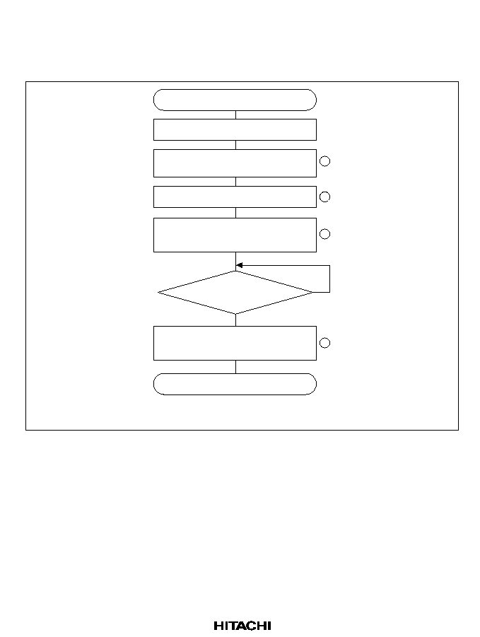
357
4. Wait for at least the interval required to transmit or receive one bit, then set TE or RE in the
serial control register (SCR) to 1. Also set RIE, TIE, TEIE and MPIE as necessary. Setting TE
or RE enables the SCI to use the TxD or RxD pin. The initial states are the mark state when
transmitting, and the idle state when receiving (waiting for a start bit).
Initialization
Clear TE and RE bits in SCR to 0
Select transmit/receive
format in SMR
Set value in BRR
Set CKE1 and CKE0 bits in SCR
(TE and RE bits are 0)
Wait
Set TE and RE bits in SCR to 1
and set RIE, TEIE, and MPIE bits
Has a 1-bit
interval elapsed?
End
1
3
4
No
Yes
2
Note: Circled numbers refer to the preceding description of the procedure in the text.
Figure 13.4 Sample Flowchart for SCI Initialization
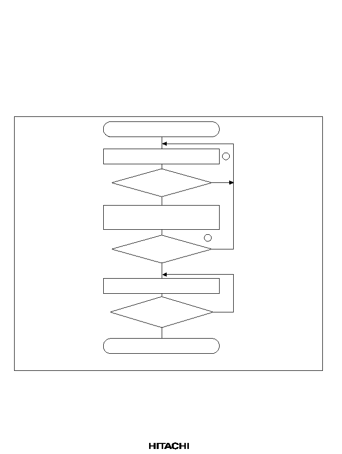
358
Transmitting Serial Data (Asynchronous Mode): Figure 13.5 shows a sample flowchart for
transmitting serial data. The procedure for transmitting serial data is as follows:
1. SCI status check and transmit data write: read the serial status register (SSR), check that the
TDRE bit is 1, then write transmit data in the transmit data register (TDR) and clear TDRE
to 0.
2. To continue transmitting serial data, read the TDRE bit to check whether it is safe to write (if it
reads 1); if so, write data in TDR, then clear TDRE to 0. When the DMAC is started by a
transmit-data-empty interrupt request (TXI) in order to write data in TDR, the TDRE bit is
checked and cleared automatically.
Start transmission
Read TDRE bit in SSR
Read TEND bit in SSR
TEND = 1?
End transmission
No
Yes
TDRE = 1?
Write transmit data to TDR and
clear TDRE bit in SSR to 0
All data transmitted?
No
Yes
Yes
No
1
2
Note: Circled numbers refer to the preceding description of the procedure in the text.
Figure 13.5 Sample Flowchart for Transmitting Serial Data

359
In transmitting serial data, the SCI operates as follows:
1. The SCI monitors the TDRE bit in SSR. When TDRE is cleared to 0, the SCI recognizes that
the transmit data register (TDR) contains new data, and loads this data from TDR into the
transmit shift register (TSR).
2. After loading the data from TDR into TSR, the SCI sets the TDRE bit to 1 and starts
transmitting. If the transmit-data-empty interrupt enable bit (TIE) is set to 1 in SCR, the SCI
requests a transmit-data-empty interrupt (TXI) at this time.
Serial transmit data is transmitted in the following order from the TxD pin:
a. Start bit: one 0-bit is output.
b. Transmit data: seven or eight bits of data are output, LSB first.
c. Parity bit or multiprocessor bit: one parity bit (even or odd parity) or one multiprocessor bit
is output. Formats in which neither a parity bit nor a multiprocessor bit is output can also
be selected.
d. Stop bit: one or two 1-bits (stop bits) are output.
e. Mark state: output of 1-bits continues until the start bit of the next transmit data.
3. The SCI checks the TDRE bit when it outputs the stop bit. If TDRE is 0, the SCI loads new
data from TDR into TSR, outputs the stop bit, then begins serial transmission of the next
frame. If TDRE is 1, the SCI sets the TEND bit to 1 in SSR, outputs the stop bit, then
continues output of 1-bits (mark state). If the transmit-end interrupt enable bit (TEIE) in SCR
is set to 1, a transmit-end interrupt (TEI) is requested.
Figure 13.6 shows an example of SCI transmit operation in asynchronous mode.
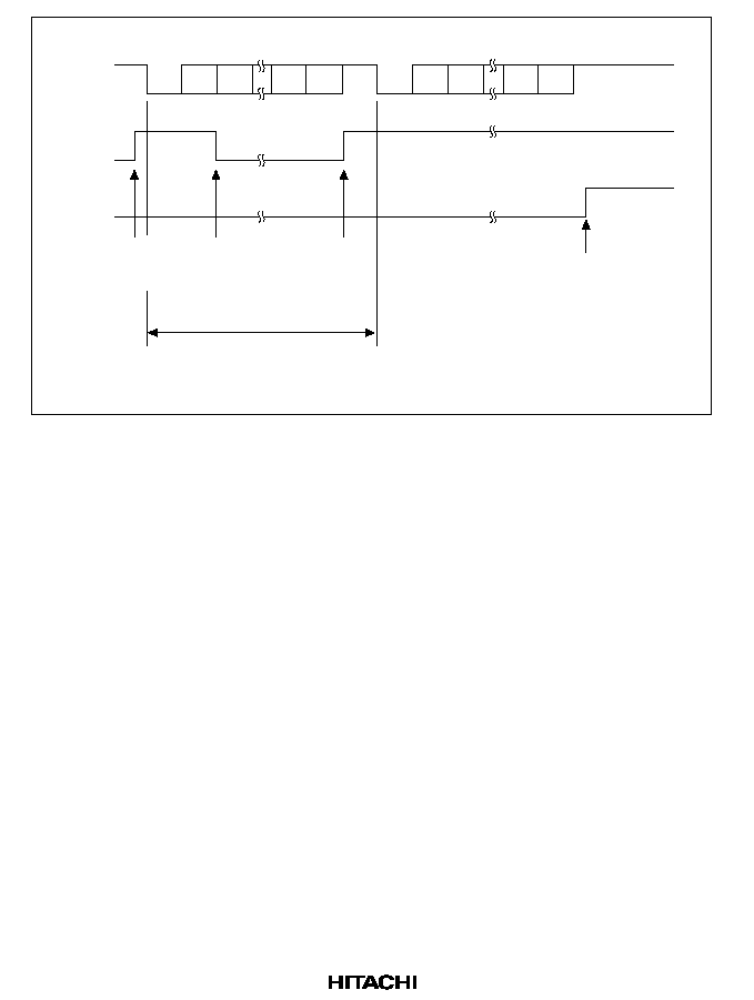
360
0
1
1
1
0/1
0
1
TDRE
TEND
Parity
bit
Parity
bit
Serial
data
Start
bit
Data
Stop
bit
Start
bit
Data
Stop
bit
Idle
(mark)
state
TXI interrupt
request
generated
TXI interrupt
request
generated
TEI interrupt
request
generated
TXI interrupt
handler writes
data to TDR
and clears
TDRE bit to 0
1 frame
D
0
D
1
D
7
D
0
D
1
D
7
0/1
Example: 8-bit data with parity and one stop bit
Figure 13.6 Example of SCI Transmit Operation in Asynchronous Mode
(8-Bit Data with Parity and One Stop Bit)
Receiving Serial Data (Asynchronous Mode): Figure 13.7 shows a sample flowchart for
receiving serial data. The procedure for receiving serial data is as follows:
1. Receive error handling: if a receive error occurs, read the ORER, PER and FER bits of the SSR
to identify the error. After executing the necessary error handling, clear ORER, PER and FER
all to 0. Receiving cannot resume if ORER, PER or FER remain set to 1.
2. SCI status check and receive-data read: read the serial status register (SSR), check that RDRF
is set to 1, then read receive data from the receive data register (RDR) and clear RDRF to 0.
The RXI interrupt can also be used to determine if the RDRF bit has changed from 0 to 1.
3. To continue receiving serial data: read the RDRF and RDR bits and clear RDRF to 0 before the
stop bit of the current frame is received. If the DMAC is started by a receive-data-full interrupt
(RXI) to read RDR, the RDRF bit is cleared automatically so this step is unnecessary.
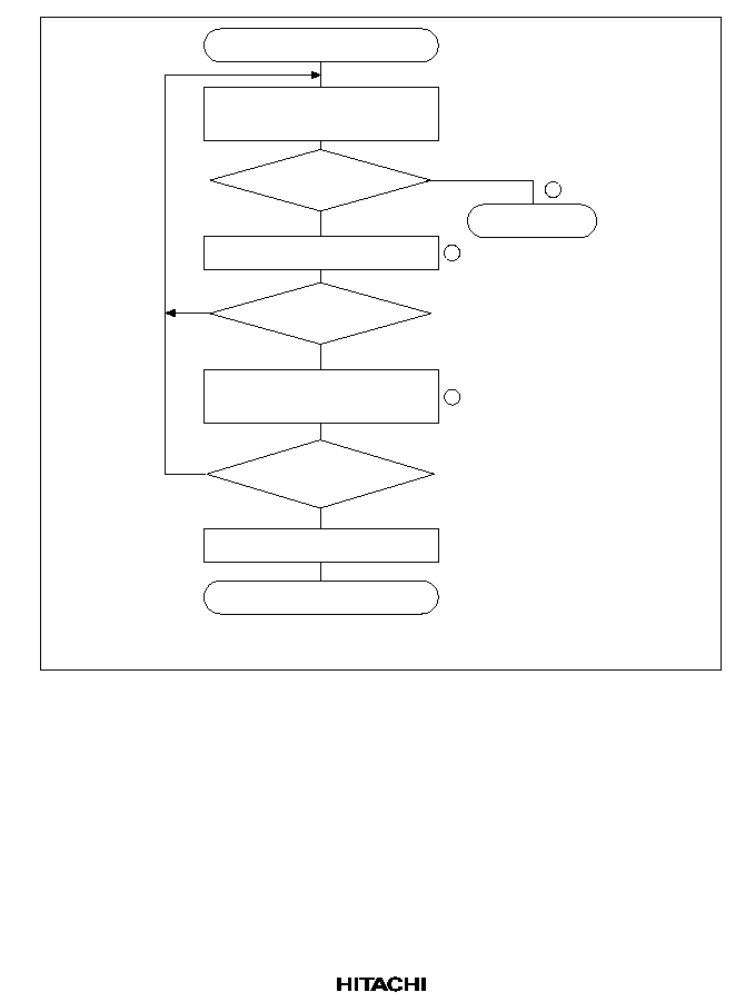
361
Start reception
Read ORER, PER, and FER
bits in SSR
All data received?
End reception
No
Yes
PER, FER, ORER = 1?
RDRF = 1?
Yes
Yes
Clear RE bit in SCR to 0
No
No
Read RDRF bit in SSR
Error handling
Read receive data in RDR, and
clear RDRF bit in SSR to 0
1
2
3
Note: Circled numbers refer to the preceding description of the procedure in the text.
Figure 13.7 Sample Flowchart for Receiving Serial Data
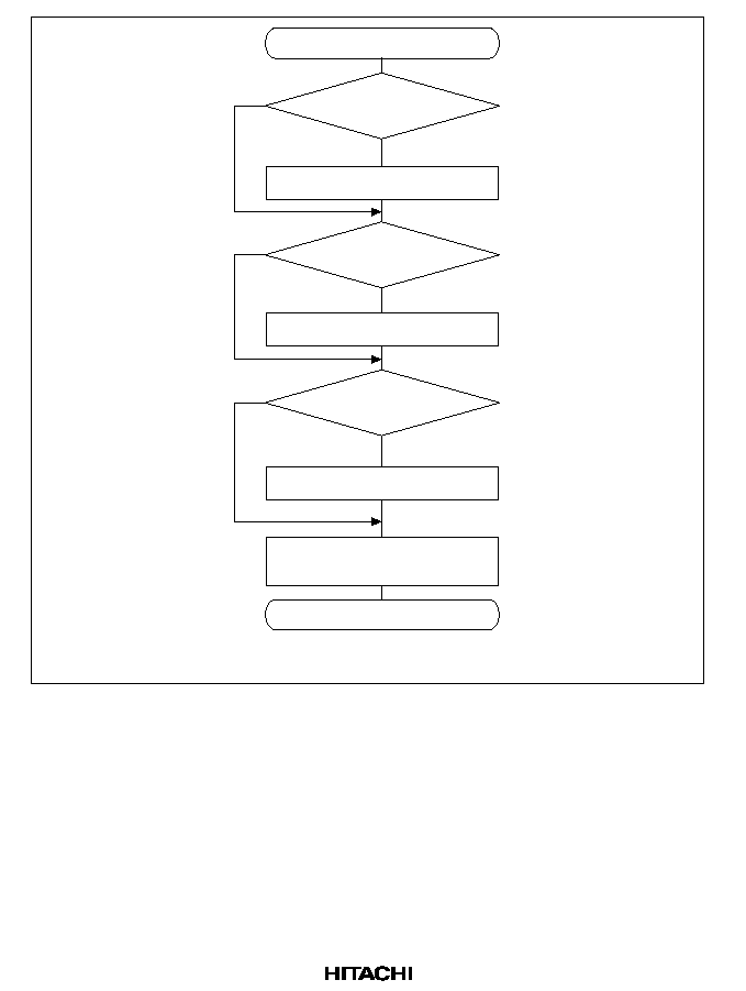
362
Error handling
ORER = 1?
Overrun error handling
FER = 1?
Yes
Framing error handling
PER = 1?
Yes
Parity error handling
Clear ORER, PER, and
FER bits in SSR to 0
End
No
No
No
Yes
Note: Circled numbers refer to the preceding description of the procedure in the text.
Figure 13.7 Sample Flowchart for Receiving Serial Data (cont)

363
In receiving, the SCI operates as follows:
1. The SCI monitors the receive data line. When it detects a start bit (0), the SCI synchronizes
internally and starts receiving.
2. Receive data is shifted into RSR in order from LSB to MSB.
3. The parity bit and stop bit are received. After receiving these bits, the SCI makes the following
checks:
a. Parity check: the number of 1s in the receive data must match the even or odd parity setting
of the O/
E bit in SMR.
b. Stop bit check: the stop bit value must be 1. If there are two stop bits, only the first stop bit
is checked.
c. Status check: RDRF must be 0 so that receive data can be loaded from RSR into RDR.
If these checks all pass, the SCI sets RDRF to 1 and stores the received data in RDR. If one of
the checks fails (receive error), the SCI operates as indicated in table 13.11.
Note:
When a receive error flag is set, further receiving is disabled. In reception, the RDRF
bit is not set to 1. Be sure to clear the error flags.
4. After setting RDRF to 1, if the receive-data-full interrupt enable bit (RIE) is set to 1 in SCR,
the SCI requests a receive-data-full interrupt (RXI). If one of the error flags (ORER, PER, or
FER) is set to 1 and the receive-data-full interrupt enable bit (RIE) in SCR is also set to 1, the
SCI requests a receive-error interrupt (ERI).
Figure 13.8 shows an example of SCI receive operation in asynchronous mode.
Table 13.12
Receive Error Conditions and SCI Operation
Receive Error
Abbreviation
Condition
Data Transfer
Overrun error
ORER
Receiving of next data ends while
RDRF is still set to 1 in SSR
Receive data not loaded
from RSR into RDR
Framing error
FER
Stop bit is 0
Receive data loaded from
RSR into RDR
Parity error
PER
Parity of receive data differs from
even/odd parity setting in SMR
Receive data loaded from
RSR into RDR
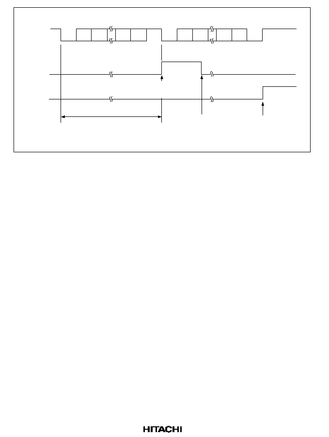
364
TDRE
FER
ERI interrupt
request generated
by framing error
1 frame
RXI interrupt
handler reads
data and clears
RDRF bit to 0
RXI interrupt
request generated
0
1
1
1
0/1
0
0
Parity
bit
Parity
bit
Serial
data
Start
bit
Data
Stop
bit
Start
bit
Data
Stop
bit
Idle
(mark)
state
D
0
D
1
D
7
D
0
D
1
D
7
0/1
Figure 13.8 Example of SCI Receive Operation
(8-Bit Data with Parity and One Stop Bit)
13.3.3
Multiprocessor Communication
The multiprocessor communication function enables several processors to share a single serial
communication line. The processors communicate in asynchronous mode using a format with an
additional multiprocessor bit (multiprocessor format).
In multiprocessor communication, each receiving processor is addressed by a unique ID. A serial
communication cycle consists of an ID-sending cycle that identifies the receiving processor, and a
data-sending cycle. The multiprocessor bit distinguishes ID-sending cycles from data-sending
cycles. The transmitting processor starts by sending the ID of the receiving processor with which it
wants to communicate as data with the multiprocessor bit set to 1. Next, the transmitting processor
sends transmit data with the multiprocessor bit cleared to 0.
Receiving processors skip incoming data until they receive data with the multiprocessor bit set to
1. When they receive data with the multiprocessor bit set to 1, receiving processors compare the
data with their IDs. The receiving processor with a matching ID continues to receive further
incoming data. Processors with IDs not matching the received data skip further incoming data
until they again receive data with the multiprocessor bit set to 1. Multiple processors can send and
receive data in this way.
Figure 13.9 shows an example of communication among processors using the multiprocessor
format.
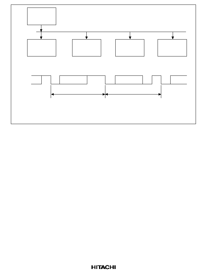
365
Receiving
processor A
(ID = 01)
(ID = 02)
(ID = 03)
(ID = 04)
Receiving
processor B
Receiving
processor C
Serial communication line
H'01
H'AA
(MPB = 0)
(MPB = 1)
ID transmit cycle =
receiving station
specification
Serial
data
Transmitting
processor
Receiving
processor D
Data transmit cycle =
data transmission to
receiving station specified
by ID
MPB: Multiprocessor bit
Figure 13.9 Example of Communication among Processors Using Multiprocessor Format
(Sending Data H'AA to Receiving Processor A)
Communication Formats: Four formats are available. Parity-bit settings are ignored when the
multiprocessor format is selected. For details see table 13.8.
Clock: See the description in the asynchronous mode section.
Transmitting Multiprocessor Serial Data: Figure 13.10 shows a sample flowchart for
transmitting multiprocessor serial data. The procedure for transmitting multiprocessor serial data is
as follows:
1. SCI status check and transmit data write: read the serial status register (SSR), check that the
TDRE bit is 1, then write transmit data in the transmit data register (TDR). Also set the MPBT
(multiprocessor bit transfer) bit to 0 or 1 in SSR. Finally, clear TDRE to 0.
2. To continue transmitting serial data, read the TDRE bit to check whether it is safe to write (if it
reads 1); if so, write data in TDR, then clear TDRE to 0. When the DMAC is started by a
transmit-data-empty interrupt request (TXI) to write data in TDR, the TDRE bit is checked and
cleared automatically.
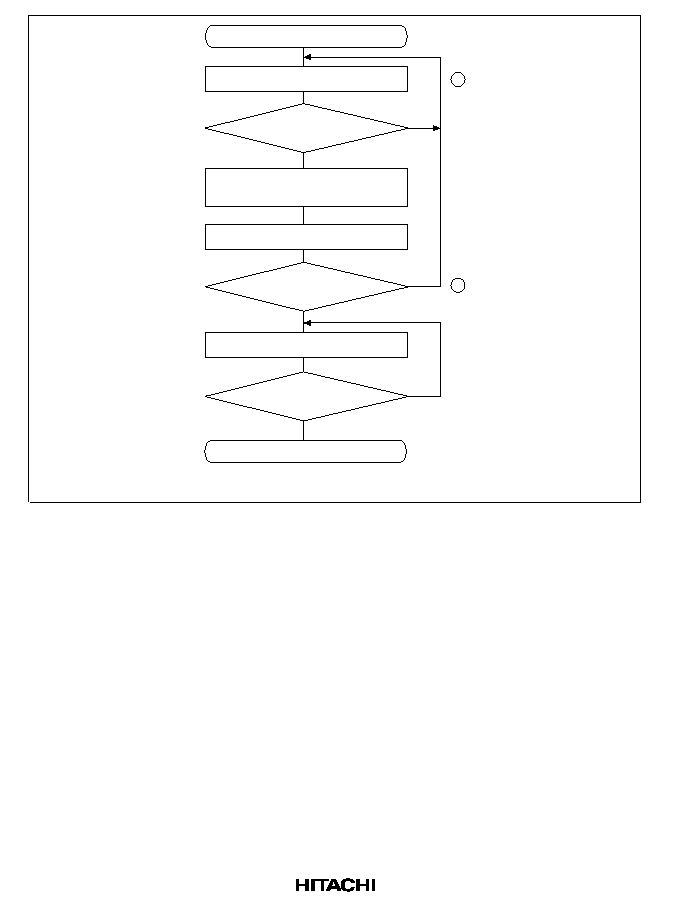
366
TDRE = 1?
Write transmit data to TDR
and set MPBT bit in SSR
Transmission ended?
Yes
TEND = 1?
Read TEND bit in SSR
Yes
End transmission
Yes
Read TDRE bit in SSR
Clear TDRE bit to 0
No
No
No
Start transmission
1
2
Note: Circled numbers refer to the preceding description of the procedure in the text.
Figure 13.10 Sample Flowchart for Transmitting Multiprocessor Serial Data
In transmitting serial data, the SCI operates as follows:
1. The SCI monitors the TDRE bit in SSR. When TDRE is cleared to 0 the SCI recognizes that
the transmit data register (TDR) contains new data, and loads this data from TDR into the
transmit shift register (TSR).
2. After loading the data from TDR into TSR, the SCI sets the TDRE bit to 1 and starts
transmitting. If the transmit-data-empty interrupt enable bit (TIE) in SCR is set to 1, the SCI
requests a transmit-data-empty interrupt (TXI) at this time.
Serial transmit data is transmitted in the following order from the TxD pin:
a. Start bit: one 0 bit is output.
b. Transmit data: seven or eight bits are output, LSB first.
c. Multiprocessor bit: one multiprocessor bit (MPBT value) is output.
d. Stop bit: one or two 1-bits (stop bits) are output.
e. Mark state: output of 1-bits continues until the start bit of the next transmit data.
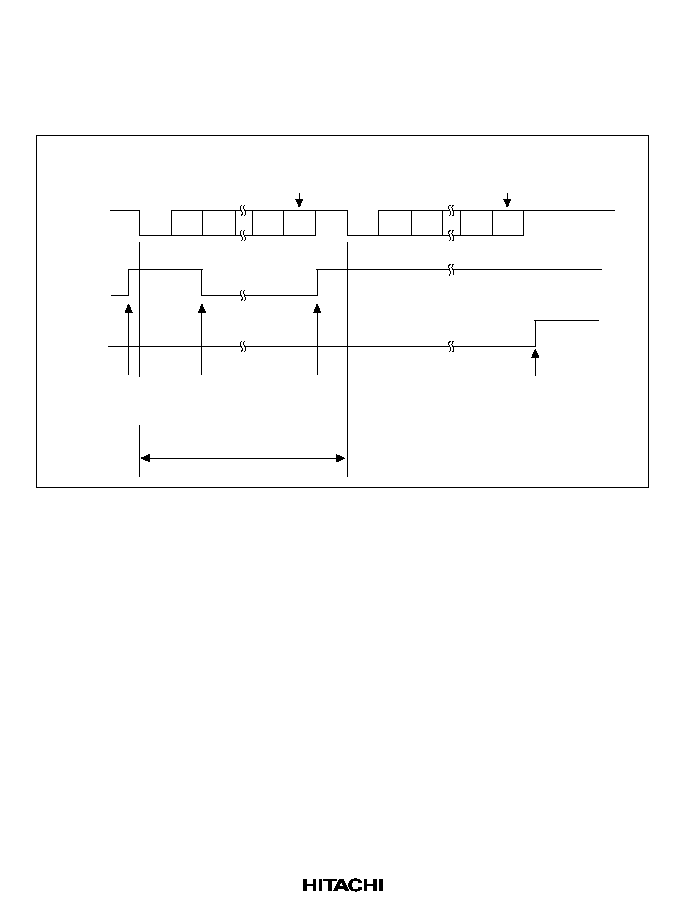
367
3. The SCI checks the TDRE bit when it outputs the stop bit. If TDRE is 0, the SCI loads data
from TDR into TSR, outputs the stop bit, then begins serial transmission of the next frame. If
TDRE is 1, the SCI sets the TEND bit in SSR to 1, outputs the stop bit, then continues output
of 1-bits in the mark state. If the transmit-end interrupt enable bit (TEIE) in SCR is set to 1, a
transmit-end interrupt (TEI) is requested at this time.
TDRE
TEND
TXI interrupt
request
generated
TXI interrupt
request
generated
TEI interrupt
request
generated
TXI interrupt
handler writes
data to TDR
and clears
TDRE bit to 0
1 frame
0
1
1
1
0/1
0
1
Multi-
processor
bit
Serial
data
Start
bit
Data
Stop
bit
Start
bit
Data
Stop
bit
Idle
(mark)
state
D
0
D
1
D
7
D
0
D
1
D
7
0/1
Multi-
processor
bit
Figure 13.11 Example of SCI Multiprocessor Transmit Operation
(8-Bit Data with Multiprocessor Bit and One Stop Bit)
Receiving Multiprocessor Serial Data: Figure 13.12 shows a sample flowchart for receiving
multiprocessor serial data. The procedure for receiving multiprocessor serial data is as follows.
1. ID receive cycle: set the MPIE bit in the serial control register (SCR) to 1.
2. SCI status check, ID reception and comparison: read the serial status register (SSR), check that
RDRF is set to 1, then read data from the receive data register (RDR) and compare with the
processor's own ID. If the ID does not match the receive data, set MPIE to 1 again and clear
RDRF to 0. If the ID matches the receive data, clear RDRF to 0.
3. Receive error handling: if a receive error occurs (figure 13.12 (cont)), read the ORER and FER
bits in SSR to identify the error. After executing the necessary error handling, clear both
ORER and FER to 0. Receiving cannot resume if ORER or FER remains set to 1. When a
framing error occurs, the RxD pin can be read to detect the break state.
4. SCI status check and data receiving: read SSR, check that RDRF is set to 1, then read data
from the receive data register (RDR).
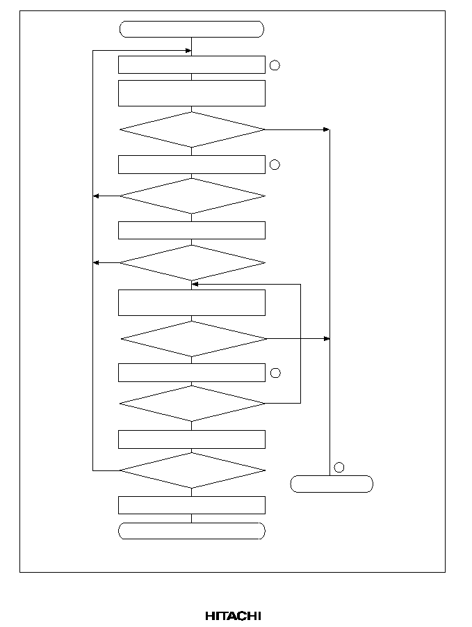
368
RDRF = 1?
FER = 1 or ORER = 1?
RDRF = 1?
All data received?
No
End reception
Yes
Set MPIE bit in SCR to 1
Read RDRF bit in SSR
Clear RE bit in SCR to 0
No
No
Read ORER and FER
bits in SSR
FER = 1 or ORER = 1?
Read RDRF bit in SSR
Read receive data in RDR
Is ID this
processor's ID?
Yes
Read ORER and FER
bits in SSR
No
Error handling
Yes
Yes
Yes
No
Start reception
No
Yes
Read receive data in RDR
1
2
4
3
Note:
Circled numbers refer to the preceding description of the procedure in the text.
Figure 13.12 Sample Flowchart for Receiving Multiprocessor Serial Data
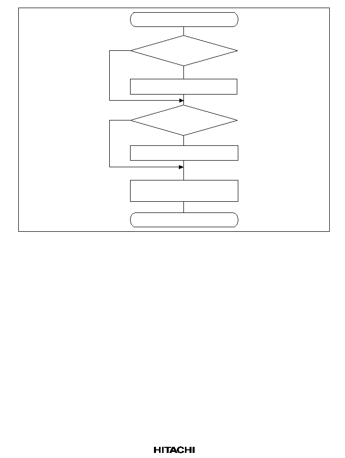
369
ORER = 1?
Yes
Framing error handling
Yes
Error handling
Overrun error handling
FER = 1?
Clear ORER and
FER bits in SSR to 0
End
No
No
Figure 13.12 Sample Flowchart for Receiving Multiprocessor Serial Data (cont)
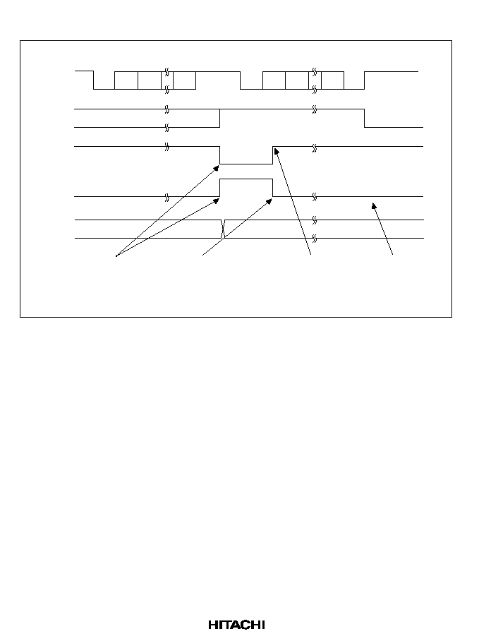
370
Figure 13.13 shows an example of SCI receive operation using a multiprocessor format.
RDRF
MPIE
RDR
value
ID1
RXI interrupt request
(multiprocessor
interrupt)
generated, MPIE = 0
RXI interrupt handler
reads RDR data
and clears RDRF
bit to 0
ID is not this
processor's ID,
so MPIE bit is
set to 1 again
No RXI
interrupt
generated;
RDR state
is held
0
1
1
1
1
0
1
Stop
bit
MPB
Serial
data
Start
bit
Data
(ID1)
Data
(data 1)
Start
bit
MPB
Stop
bit
Idle
(mark)
state
D
0
D
1
D
7
D
0
D
1
D
7
0
MPB
Figure 13.13 Example of SCI Receive Operation
(Own ID Does Not Match Data, 8-Bit Data with Multiprocessor Bit and One Stop Bit)
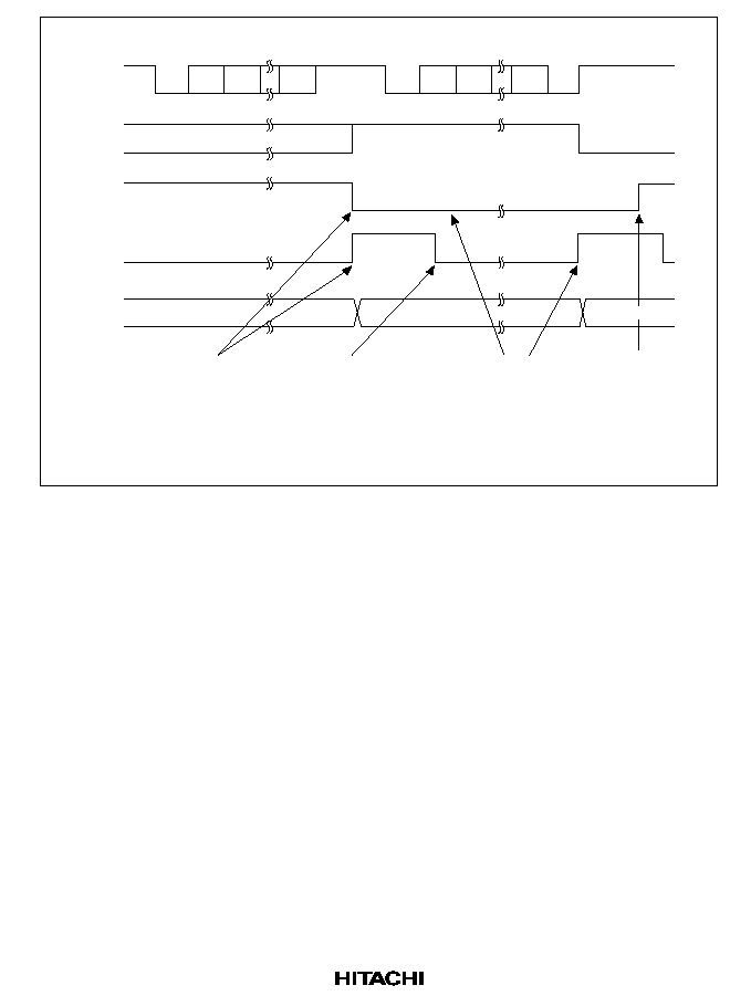
371
RDRF
MPIE
RDR
value
ID1
ID2
Data2
0
1
1
1
1
0
1
MPB
MPB
Serial
data
Start
bit
Data
(ID2)
Data
(Data 2)
Stop
bit
Start
bit
Stop
bit
Idling
(marking)
D
0
D
1
D
7
D
0
D
1
D
7
0
RXI interrupt
request
(multiprocessor
interrupt)
generated,
MPIE = 0
RXI interrupt
handler
reads RDR data
and clears
RDRF bit to 0
ID is that of
this processor,
so reception
continues unchanged
and data is received
by the RXI interrupt
handler
MPIE
bit set to 1
again
MPB
Figure 13.13 Example of SCI Receive Operation
(Own ID Matches Data, 8-Bit Data with Multiprocessor Bit and One Stop Bit) (cont)
13.3.4
Clocked Synchronous Operation
In clocked synchronous mode, the SCI transmits and receives data in synchronization with clock
pulses. This mode is suitable for high-speed serial communication.
The SCI transmitter and receiver are independent, so full duplex communication is possible while
sharing the same clock. The transmitter and receiver are also double buffered, so continuous
transmitting or receiving is possible by reading or writing data while transmitting or receiving is in
progress.
Figure 13.14 shows the general format in clocked synchronous serial communication.
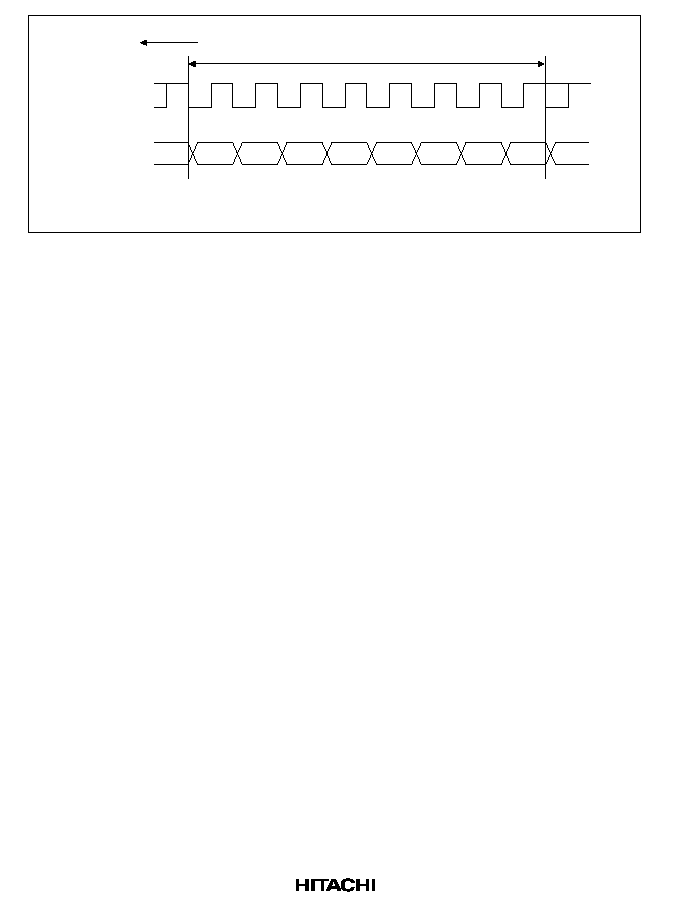
372
Bit 0
Bit 1
Bit 2
Bit 3
Bit 4
Bit 5
Bit 6
Bit 7
LSB
MSB
Serial clock
Serial data
*
*
Transfer direction
One unit of communication data (character or frame)
Note: High except in continuous transmitting or receiving.
Figure 13.14 Data Format in Clocked Synchronous Communication
In clocked synchronous serial communication, each data bit is output on the communication line
from one falling edge of the serial clock to the next. Data is guaranteed valid at the rising edge of
the serial clock. In each character, the serial data bits are transmitted in order from LSB (first) to
MSB (last). After output of the MSB, the communication line remains in the state of the MSB. In
clocked synchronous mode, the SCI transmits or receives data by synchronizing with the falling
edge of the serial clock.
Communication Format: The data length is fixed at eight bits. No parity bit or multiprocessor bit
can be added.
Clock: An internal clock generated by the built-in baud rate generator or an external clock input
from the SCK pin can be selected as the SCI transmit/receive clock. The clock source is selected
by the C/
A bit in the serial mode register (SMR) and bits CKE1 and CKE0 in the serial control
register (SCR). See table 13.9.
When the SCI operates on an internal clock, it outputs the clock signal at the SCK pin. Eight clock
pulses are output per transmitted or received character. When the SCI is not transmitting or
receiving, the clock signal remains in the high state.
Figure 13.15 shows an example of SCI transmit operation. In transmitting serial data, the SCI
operates as follows.
1. The SCI monitors the TDRE bit in SSR. When TDRE is cleared to 0 the SCI recognizes that
the transmit data register (TDR) contains new data and loads this data from TDR into the
transmit shift register (TSR).
2. After loading the data from TDR into TSR, the SCI sets the TDRE bit to 1 and starts
transmitting. If the transmit-data-empty interrupt enable bit (TIE) in SCR is set to 1, the SCI
requests a transmit-data-empty interrupt (TXI) at this time.
If clock output mode is selected, the SCI outputs eight synchronous clock pulses. If an external
clock source is selected, the SCI outputs data in synchronization with the input clock. Data is
output from the TxD pin in order from LSB (bit 0) to MSB (bit 7).
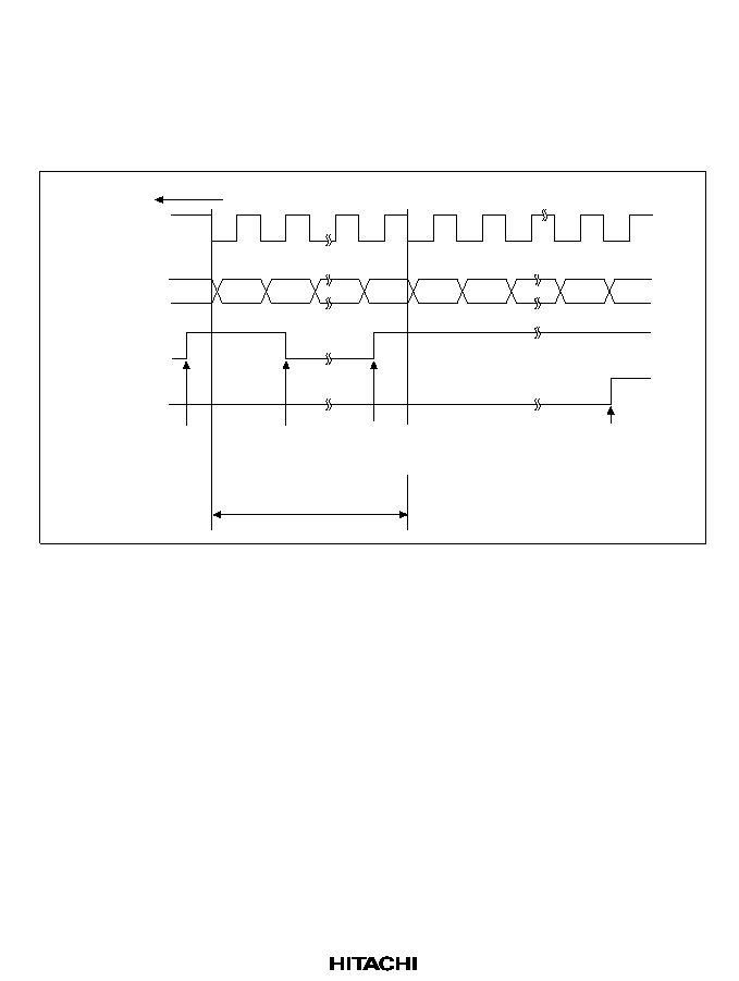
373
3. The SCI checks the TDRE bit when it outputs the MSB (bit 7). If TDRE is 0, the SCI loads
data from TDR into TSR, transmits the MSB, then begins serial transmission of the next frame.
If TDRE is 1, the SCI sets the TEND bit in SSR to 1, transmits the MSB, then holds the
transmit data pin (TxD) in the MSB state. If the transmit-end interrupt enable bit (TEIE) in
SCR is set to 1, a transmit-end interrupt (TEI) is requested at this time.
4. After the end of serial transmission, the SCK pin is held in the high state.
Bit 0
Bit 1
Bit 7
Bit 0
Bit 1
Bit 6
Serial clock
Serial data
Transfer direction
Bit 7
TXI interrupt
handler writes data
to TDR and clears
TDRE bit to 0
1 frame
TDRE
TEND
LSB
MSB
TXI interrupt
request
generated
TXI interrupt
request
generated
TEI interrupt
request
generated
Figure 13.15 Example of SCI Transmit Operation
Transmitting and Receiving Data
SCI Initialization (Clocked Synchronous Mode): Before transmitting or receiving, software
must clear the TE and RE bits to 0 in the serial control register (SCR), then initialize the SCI as
follows.
When changing the mode or communication format, always clear the TE and RE bits to 0 before
following the procedure given below. Clearing TE to 0 sets TDRE to 1 and initializes the transmit
shift register (TSR). Clearing RE to 0, however, does not initialize the RDRF, PER, FER, and
ORER flags and receive data register (RDR), which retain their previous contents.
Figure 13.16 shows a sample flowchart for initializing the SCI. The procedure for initializing the
SCI is as follows.
1. Select the communication format in the serial mode register (SMR).
2. Write the value corresponding to the bit rate in the bit rate register (BRR) unless an external
clock is used.
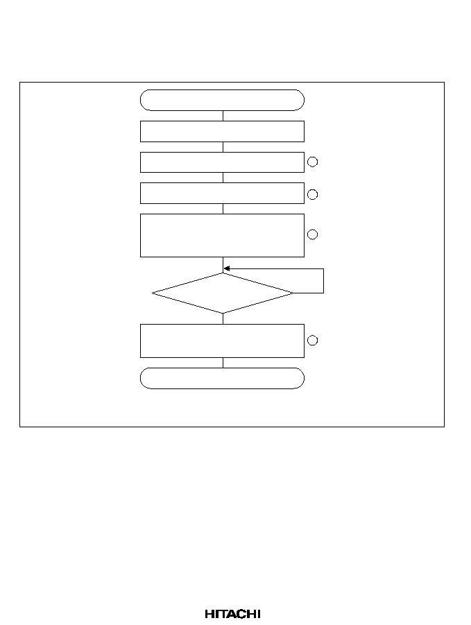
374
3. Select the clock source in the serial control register (SCR). Leave RIE, TIE, TEIE, MPIE, TE
and RE cleared to 0.
4. Wait for at least the interval required to transmit or receive one bit, then set TE or RE in the
serial control register (SCR) to 1. Also set RIE, TIE, TEIE and MPIE.
Initialization
Clear TE and RE bits in SCR to 0
Has a 1-bit
period elapsed?
Set TE and RE bits in SCR to 1 and
set RIE, TIE, TEIE, and MPIE bits
Set transmit/receive format in SMR
Yes
No
Set value in BRR
Set RIE, TIE, TEIE, MPIE, CKE1,
and CKE0 bits in SCR
(TE and RE are 0)
End
Wait
1
2
3
4
Note: Circled numbers refer to the preceding description of the procedure in the text.
Figure 13.16 Sample Flowchart for SCI Initialization
Transmitting Serial Data (Clocked Synchronous Mode): Figure 13.17 shows a sample
flowchart for transmitting serial data. The procedure for transmitting serial data is as follows.
1. SCI status check and transmit data write: read the serial status register (SSR), check that the
TDRE bit is 1, then write transmit data in the transmit data register (TDR) and clear TDRE
to 0.
2. To continue transmitting serial data, read the TDRE bit to check whether it is safe to write (if it
reads 1); if so, write data in TDR, then clear TDRE to 0. When the DMAC is started by a
transmit-data-empty interrupt request (TXI) to write data in TDR, the TDRE bit is checked and
cleared automatically.
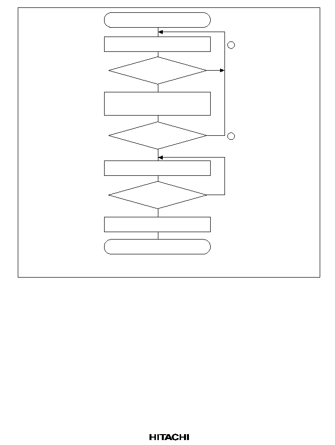
375
Start transmission
Read TDRE bit in SSR
All data transmitted?
Yes
No
End transmission
TDRE = 1?
Write transmssion data to TDR
and clear TDRE bit in SSR to 0
Yes
No
Read TEND bit in SSR
TEND = 1?
Yes
No
Clear TE bit in SCR to 0
1
2
Note:
Circled numbers refer to the preceding description of the procedure in the text.
Figure 13.17 Sample Flowchart for Serial Transmitting
Receiving Serial Data (Clocked Synchronous Mode): Figure 13.18 shows a sample flowchart
for receiving serial data. When switching from asynchronous mode to clocked synchronous mode,
make sure that ORER, PER, and FER are cleared to 0. If PER or FER is set to 1, the RDRF bit
will not be set and both transmitting and receiving will be disabled. Figure 13.19 shows an
example of the SCI receive operation.
The procedure for receiving serial data is as follows:
1. Receive error handling: if a receive error occurs, read the ORER bit in SSR to identify the
error. After executing the necessary error handling, clear ORER to 0. Transmitting/receiving
cannot resume if ORER remains set to 1.
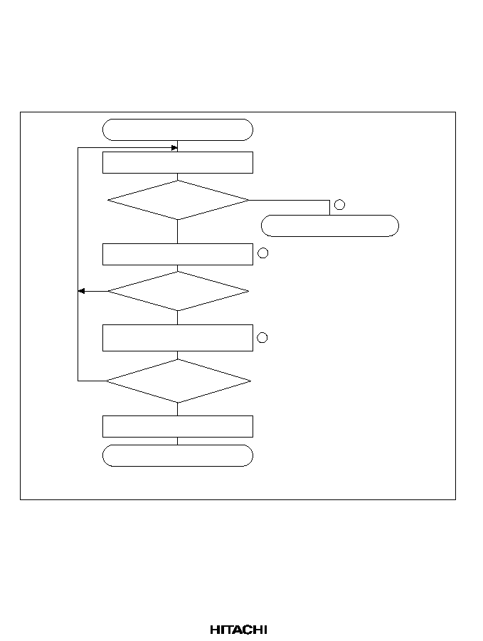
376
2. SCI status check and receive data read: read the serial status register (SSR), check that RDRF
is set to 1, then read receive data from the receive data register (RDR) and clear RDRF to 0.
The RXI interrupt can also be used to determine if the RDRF bit has changed from 0 to 1.
3. To continue receiving serial data: read RDR, and clear RDRF to 0 before the MSB (bit 7) of
the current frame is received. If the DMAC is started by a receive-data-full interrupt (RXI) to
read RDR, the RDRF bit is cleared automatically so this step is unnecessary.
Read ORER bit in SSR
All data received?
End reception
No
Yes
ORER = 1?
RDRF = 1?
Yes
Clear RE bit in SCR to 0
No
No
Read RDRF bit in SSR
Yes
Error processing
Read receive data in RDR and
clear RDRF bit in SSR to 0
Start reception
1
2
3
Note:
Circled numbers refer to the preceding description of the procedure in the text.
Figure 13.18 Sample Flowchart for Serial Receiving
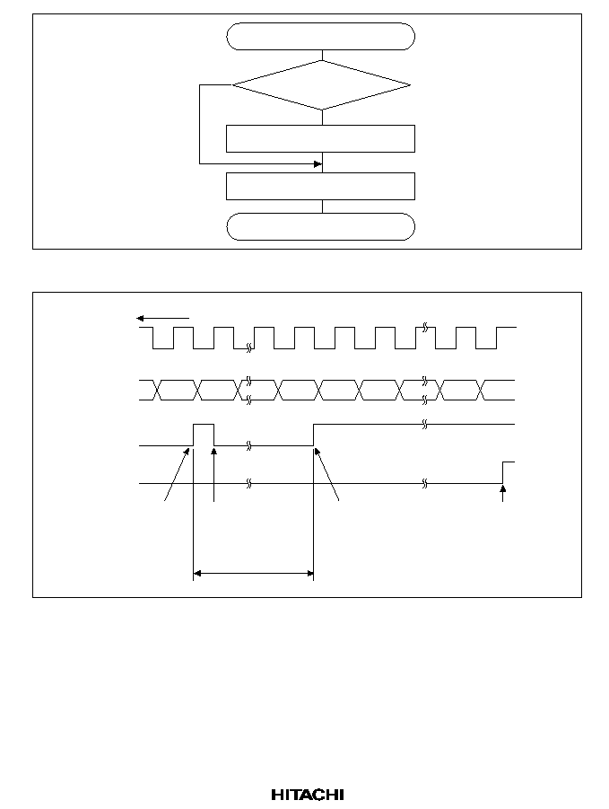
377
Error handling
End
ORER = 1?
No
Clear ORER bit in SSR to 0
Yes
Overrun error handling
Figure 13.18 Sample Flowchart for Serial Receiving (cont)
Bit 7
Bit 0
Bit 7
Bit 0
Bit 1
Bit 6
Serial clock
Serial
data
Transfer direction
Bit 7
RXI interrupt
handler reads
data and clears
RDRF bit to 0
1 frame
RXI interrupt
request
generated
RXI interrupt
request
generated
ERI interrupt
request
generated
by overrun
error
RDRF
ORER
Figure 13.19 Example of SCI Receive Operation

378
In receiving, the SCI operates as follows:
1. The SCI synchronizes with serial clock input or output and initializes internally.
2. Receive data is shifted into RSR in order from LSB to MSB. After receiving the data, the SCI
checks that RDRF is 0 so that receive data can be loaded from RSR into RDR. If this check
passes, the SCI sets RDRF to 1 and stores the received data in RDR. If the check does not pass
(receive error), the SCI operates as indicated in table 13.8. The RDRF bit is not set to 1. Be
sure to clear the error flag.
3. After setting RDRF to 1, if the receive-data-full interrupt enable bit (RIE) is set to 1 in SCR,
the SCI requests a receive-data-full interrupt (RXI). If the ORER bit is set to 1 and the receive-
data-full interrupt enable bit (RIE) in SCR is also set to 1, the SCI requests a receive-error
interrupt (ERI).
Transmitting and Receiving Serial Data Simultaneously (Clocked Synchronous Mode):
Figure 13.20 shows a sample flowchart for transmitting and receiving serial data simultaneously.
The procedure for transmitting and receiving serial data simultaneously is as follows:
1. SCI status check and transmit data write: read the serial status register (SSR), check that the
TDRE bit is 1, then write transmit data in the transmit data register (TDR) and clear TDRE to
0. The TXI interrupt can also be used to determine if the TDRE bit has changed from 0 to 1.
2. Receive error handling: if a receive error occurs, read the ORER bit in SSR to identify the
error. After executing the necessary error handling, clear ORER to 0. Transmitting/receiving
cannot resume if ORER remains set to 1.
3. SCI status check and receive data read: read the serial status register (SSR), check that RDRF
is set to 1, then read receive data from the receive data register (RDR) and clear RDRF to 0.
The RXI interrupt can also be used to determine if the RDRF bit has changed from 0 to 1.
4. To continue transmitting and receiving serial data: read the RDRF bit and RDR, and clear
RDRF to 0 before the MSB (bit 7) of the current frame is received. Also read the TDRE bit to
check whether it is safe to write (if it reads 1); if so, write data in TDR, then clear TDRE to 0
before the MSB (bit 7) of the current frame is transmitted. When the DMAC is started by a
transmit-data-empty interrupt request (TXI) to write data in TDR, the TDRE bit is checked and
cleared automatically. When the DMAC is started by a receive-data-full interrupt (RXI) to read
RDR, the RDRF bit is cleared automatically.
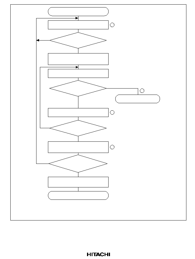
379
Start transmission/reception
Read TDRE bit in SSR
All data
transmitted/received?
End transmission/reception
No
Yes
TDRE = 1?
Write transmit data to TDR
and clear TDRE bit in SSR to 0
RDRF = 1?
No
Yes
Yes
No
Read ORER bit in SSR
Error handling
ORER = 1?
No
Read RDRF bit in SSR
Yes
Read receive data in RDR
and clear RDRF bit in SSR to 0
Clear TE and RE bits
in SCR to 0
1
2
3
4
Note: When switching from transmitting or receiving to simultaneous transmitting and receiving,
clear both TE and RE to 0, then set both TE and RE to 1.
Circled numbers refer to the preceding description of the procedure in the text.
Figure 13.20 Sample Flowchart for Serial Transmitting

380
13.4
SCI Interrupt Sources and the DMAC
The SCI has four interrupt sources in each channel: transmit-end (TEI), receive-error (ERI),
receive-data-full (RXI), and transmit-data-empty (TXI). Table 13.13 lists the interrupt sources and
indicates their priority. These interrupts can be enabled and disabled by the TIE, RIE, and TEIE
bits in the serial control register (SCR). Each interrupt request is sent separately to the interrupt
controller.
TXI is requested when the TDRE bit in SSR is set to 1. TXI can start the direct memory access
controller (DMAC) to transfer data. TDRE is automatically cleared to 0 when the DMAC writes
data in the transmit data register (TDR).
RXI is requested when the RDRF bit in SSR is set to 1. RXI can start the DMAC to transfer data.
RDRF is automatically cleared to 0 when the DMAC reads the receive data register (RDR).
ERI is requested when the ORER, PER, or FER bit in SSR is set to 1. ERI cannot start the DMAC.
TEI is requested when the TEND bit in SSR is set to 1. TEI cannot start the DMAC. Where the
TXI interrupt indicates that transmit data writing is enabled, the TEI interrupt indicates that the
transmit operation is complete.
Table 13.13
SCI Interrupt Sources
Interrupt Source
Description
DMAC Availability
Priority
ERI
Receive error (ORER, PER, or FER)
No
High
RXI
Receive data register full (RDRF)
Yes
TXI
Transmit data register empty (TDRE)
Yes
TEI
Transmit end (TEND)
No
Low
See section 4, Exception Handling, for information on the priority order and relationship to non-
SCI interrupts.
13.5
Usage Notes
Note the following points when using the SCI.
TDR Write and TDRE Flag: The TDRE bit in the serial status register (SSR) is a status flag
indicating loading of transmit data from TDR into TSR. The SCI sets TDRE to 1 when it transfers
data from TDR to TSR. Data can be written to TDR regardless of the TDRE bit status. If new data
is written in TDR when TDRE is 0, however, the old data stored in TDR will be lost because the
data has not yet been transferred to TSR. Before writing transmit data to TDR, be sure to check
that TDRE is set to 1.

381
Simultaneous Multiple Receive Errors: Table 13.14 indicates the state of the SSR status flags
when multiple receive errors occur simultaneously. When an overrun error occurs, the RSR
contents cannot be transferred to RDR, so receive data is lost.
Table 13.14
SSR Status Flags and Transfer of Receive Data
SSR Status Flags
Receive Data
Transfer
Receive Error Status
RDRF
ORER
FER
PER
RSR
RDR
Overrun error
1
1
0
0
X
Framing error
0
0
1
0
O
Parity error
0
0
0
1
O
Overrun error + framing error
1
1
1
0
X
Overrun error + parity error
1
1
0
1
X
Framing error + parity error
0
0
1
1
O
Overrun error + framing error + parity
error
1
1
1
1
X
O: Receive data is transferred from RSR to RDR.
X: Receive data is not transferred from RSR to RDR.
Break Detection and Processing: In the break state, the input from the RxD pin consists of all 0s,
so FER is set and the parity error flag (PER) may also be set. In the break state, the SCI receiver
continues to operate, so if the FER bit is cleared to 0, it will be set to 1 again.
Receive Error Flags and Transmitter Operation (Clocked Synchronous Mode Only): When a
receive error flag (ORER, PER, or FER) is set to 1, the SCI will not start transmitting even if
TDRE is set to 1. Be sure to clear the receive error flags to 0 before starting to transmit. Note that
clearing RE to 0 does not clear the receive error flags.
Receive Data Sampling Timing and Receive Margin in Asynchronous Mode: In asynchronous
mode, the SCI operates on a base clock of 16 times the bit rate frequency. In receiving, the SCI
synchronizes internally with the falling edge of the start bit, which it samples on the base clock.
Receive data is latched on the rising edge of the eighth base clock pulse. See figure 13.21.
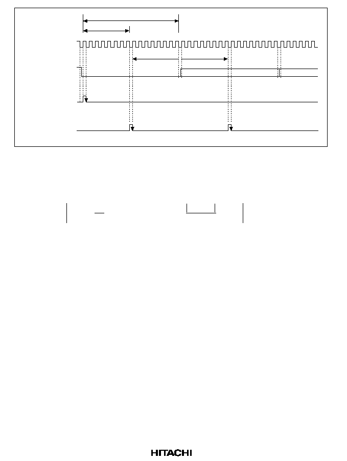
382
0 1 2 3 4 5 6 7 8 9 10111213 1415 0 1 2 3 4 5 6 7 8 9 10111213 1415 0 1 2 3 4 5
CLK
Receive
data (RxD)
Synchronization
sampling
timing
Data
sampling
timing
8 clocks
16 clocks
Start bit
7.5 clocks
+7.5 clocks
D0
D1
Figure 13.21 Receive Data Sampling Timing in Asynchronous Mode
The receive margin in asynchronous mode can therefore be expressed as in equation 1.
Equation 1:
M = 0. 5
1
2N
1
L 0. 5
(
)
F
D 0. 5
N
(1 + F)
×
100%
M : Receive margin (%)
N : Ratio of clock frequency to bit rate (N = 16)
D : Clock duty cycle (D = 01.0)
L : Frame length (L = 912)
F : Absolute deviation of clock frequency
From equation (1), if F = 0 and D = 0.5 the receive margin is 46.875%, as given by equation 2.
Equation 2:
D
= 0.5, F = 0
M = (0.5 1/(2
×
16))
×
100%
= 46.875%
This is a theoretical value. A reasonable margin to allow in system designs is 2030%.
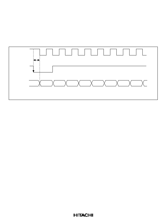
383
Constraints on DMAC Use:
·
When using an external clock source for the serial clock, update TDR with the DMAC, and
then after twenty system clock cycles or more elapse, input a transmit clock. If a transmit clock
is input in the first four states after TDR is written, an error may occur (figure 13.22).
·
Before reading the receive data register (RDR) with the DMAC, select the receive-data-full
interrupt of the SCI as an activation source using the resource select bit (RS) in the channel
control register (CHCR).
D0
D1
D2
D3
D4
D5
D6
D7
SCK
TDRE
t
Note: During external clock operation, an error may occur if t is 4 states or less.
Figure 13.22 Example of Clocked Synchronous Transmission with DMAC
Cautions for Clocked Synchronous External Clock Mode:
·
Set TE = RE = 1 only when external clock SCK is 1.
·
Do not set TE = RE = 1 until at least four clock cycles after external clock SCK has changed
from 0 to 1.
·
When receiving, RDRF is set to 1 when RE is cleared to 0 2.53.5 clocks after the rising edge
of the RxD D7 bit SCK input, but it cannot be copied to RDR.
Caution for Clocked Synchronous Internal Clock Mode: When receiving, RDRF is set to 1
when RE is cleared to 0 1.5 clocks after the rising edge of the RxD D7 bit SCK output, but it
cannot be copied to RDR.

384

385
Section 14 Power-Down Modes
14.1
Overview
The SH7604 has a module standby function (which selectively halts operation of some on-chip
peripheral modules), a sleep mode (which halts CPU function), and a standby mode (which halts
all functions).
14.1.1
Power-Down Modes
In addition to the sleep mode and standby mode, the SH7604 also has a third power-down mode,
the module standby function, which halts the DMAC, multiplication unit, division unit, free-
running timer, and SCI on-chip peripheral modules.
Table 14.1 shows the transition conditions for entering the modes from the program execution
state, as well as the CPU and peripheral module states in each mode and the procedures for
canceling each mode.

386
Table 14.1
Power-Down Modes
State
Mode
Transition
Condition
Clock
CPU,
MULT,
Cache
UBC,
BSC
FRT, SCI,
DMAC, DIV,
INTC, WDT, Pins
Canceling
Procedure
Sleep
mode
SLEEP
instruction
executed with
SBY bit set to 0
in SBYCR
Runs
Halted
Runs
Runs
Runs
1. Interrupt
2. DMA
address
error
3. Power-
on reset
4. Manual
reset
Standby
mode
SLEEP
instruction
executed with
SBY bit set to 1
in SBYCR
Halted
Halted
Held
Halted
Held or high
impedance
1. NMI
interrupt
2. Power-
on reset
3. Manual
reset
Module
standby
function
MSTP bit for
relevant module
is set to 1
Runs
Run
(MULT
is held)
Runs
When
MSTP bit
is 1, the
supply of
the clock to
the relevant
module is
halted.
FRT and
SCI pins
are
initialized,
and others
operate.
Clear MSTP
bit to 0
14.1.2
Register
Table 14.2 shows the register configuration.
Table 14.2
Register Configuration
Name
Abbreviation
R/W
Initial Value
Address
Standby control register
SBYCR
R/W
H'60
H'FFFFFE91

387
14.2
Description of Register
14.2.1
Standby Control Register (SBYCR)
The standby control register (SBYCR) is an 8-bit read/write register that sets the power-down
mode. SBYCR is initialized to H'00 by a reset.
Bit:
7
6
5
4
3
2
1
0
Bit name:
SBY
HIZ
--
MSTP4
MSTP3
MSTP2
MSTP1
MSTP0
Initial value:
0
0
0
0
0
0
0
0
R/W:
R/W
R/W
--
R/W
R/W
R/W
R/W
R/W
·
Bit 7--Standby (SBY): Specifies transition to standby mode. The SBY bit cannot be set to 1
while the watchdog timer is running (when the TME bit in the WDt's WTCSR register is 1).
To enter the standby mode, halt the WDT (set the TME bit in WTCSR to 0) and set the SBY
bit.
Bit 7: SBY
Description
0
Executing a SLEEP instruction puts the chip into sleep mode
(Initial value)
1
Executing a SLEEP instruction puts the chip into standby mode
·
Bit 6--Port High Impedance (HIZ): Selects whether output pins are set to high impedance or
retain the output state in standby mode. When HIZ = 0 (initial state), the specified pin retains
its output state. When HIZ = 1, the pin goes to the high-impedance state. See Appendix A.1,
Pin States during Resets, Power-Down States and Bus Release State, for which pins are
controlled.
Bit 6: HIZ
Description
0
Pin state retained in standby mode
(Initial value)
1
Pin goes to high impedance in standby mode
·
Bit 5--Reserved: This bit always reads 0. The write value should always be 0.
·
Bit 4: Module stop 4 (MSTP4): Specifies halting the clock supply to the DMAC. When
MSTP4 bit is set to 1, the supply of the clock to the DMAC is halted. When the clock halts, the
DMAC retains its pre-halt state. When MSTP4 is cleared to 0 and the DMAC begins running
again, its starts operating from its pre-halt state. Set this bit while the DMAC is halted; this bit
cannot be set while the DMAC is operating (transferring data).

388
Bit 4: MSTP4
Description
0
DMAC running
(Initial value)
1
Clock supply to DMAC halted
·
Bit 3--Module Stop 3 (MSTP3): Specifies halting the clock supply to the multiplication unit
(MULT). When the MSTP3 bit is set to 1, the supply of the clock to MULT is halted. When
the clock halts, MULT retains its pre-halt state. This bit should be set when the MULT is
halted.
Bit 3: MSTP3
Description
0
MULT running
(Initial value)
1
Clock supply to MULT halted
·
Bit 2--Module Stop 2 (MSTP2): Specifies halting the clock supply to the division unit
(DIVU). When the MSTP2 bit is set to 1, the supply of the clock to DIVU is halted. When the
clock halts, the DIVU registers retain their pre-halt state. This bit should be set when the DIVU
is halted.
Bit 2: MSTP2
Description
0
DIVU running
(Initial value)
1
Clock supply to DIVU halted
·
Bit 1--Module Stop 1 (MSTP1): Specifies halting the clock supply to the 16-bit free-running
timer (FRT). When the MSTP1 bit is set to 1, the supply of the clock to the FRT is halted.
When the clock halts, all FRT registers are initialized except the FRT interrupt vector register
in INTC, which holds its previous value. When MSTP1 is cleared to 0 and the FRT begins
running again, its starts operating from its initial state.
Bit 1: MSTP1
Description
0
FRT running
(Initial value)
1
Clock supply to FRT halted
·
Bit 0--Module Stop 0 (MSTP0): Specifies halting the clock supply to the serial
communication interface (SCI). When the MSTP0 bit is set to 1, the supply of the clock to the
SCI is halted. When the clock halts, all SCI registers are initialized except the SCI interrupt
vector register in INTC, which holds its previous value. When MSTP0 is cleared to 0 and the
SCI begins running again, its starts operating from its initial state.

389
Bit 0: MSTP0
Description
0
SCI running
(Initial value)
1
Clock supply to SCI halted
14.3
Sleep Mode
14.3.1
Transition to Sleep Mode
Executing the SLEEP instruction when the SBY bit in SBYCR is 0 causes a transition from the
program execution state to sleep mode. Although the CPU halts immediately after executing the
SLEEP instruction, the contents of its internal registers remain unchanged. The on-chip peripheral
modules continue to run in sleep mode.
14.3.2
Canceling Sleep Mode
Sleep mode is canceled by an interrupt, DMA address error, power-on reset, or manual reset.
Cancellation by an Interrupt: When an interrupt occurs, sleep mode is canceled and interrupt
exception handling is executed. Sleep mode is not canceled if the interrupt cannot be accepted
because its priority level is equal to or less than the mask level set in the CPU's status register
(SR) or if an interrupt by an on-chip peripheral module is disabled at the peripheral module.
Cancellation by a DMA Address Error: If a DMA address error occurs, sleep mode is canceled
and DMA address error exception handling is executed.
Cancellation by a Power-On Reset: A power-on reset cancels sleep mode.
Cancellation by a Manual Reset: A manual reset cancels sleep mode.
14.4
Standby Mode
14.4.1
Transition to Standby Mode
To enter standby mode, set the SBY bit to 1 in SBYCR, then execute the SLEEP instruction. The
chip switches from the program execution state to standby mode. The NMI interrupt cannot be
accepted when the SLEEP instruction is executed, or for the following five cycles. In standby
mode, power consumption is greatly reduced by halting not only the CPU, but the clock and on-
chip peripheral modules as well. CPU register contents are held, and some on-chip peripheral
modules are initialized.

390
Table 14.3
Register States in Standby Mode
Module
Registers Initialized
Registers that Retain
Data
Registers with
Undefined Contents
Interrupt controller
(INTC)
--
All registers
--
User break controller
(UBC)
--
All registers
--
Bus state controller
(BSC)
--
All registers
--
DMAC
DMA channel control
register 0
DMA channel control
register 1
DMA operation register
All registers except DMA
channel control register
0, DMA channel control
register 1, and DMA
operation register
--
DIVU
--
--
All registers
Watchdog timer (WDT)
Bits 75 of the timer
control/status register
Bits 20 of the timer
control/status register
--
Reset control/status
register
Timer counter
16-bit free-running timer
(FRT)
All registers
--
--
Serial communication
interface (SCI)
All registers
--
--
Others
--
Standby control register
Frequency modification
register
--
14.4.2
Canceling Standby Mode
Standby mode is canceled by an NMI interrupt, a power-on reset, or a manual reset.
Cancellation by an NMI: When a rising edge or falling edge is detected in the NMI signal, after
the elapse of the time set in the WDT timer control/status register, clocks are supplied to the entire
chip, standby mode is canceled, and NMI exception handling begins.
Cancellation by a Power-On Reset: A power-on reset cancels standby mode.
Cancellation by a Manual Reset: A manual reset cancels standby mode.
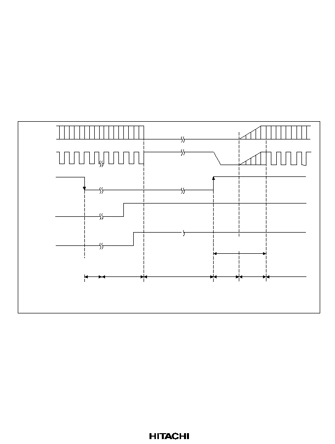
391
14.4.3
Standby Mode Cancellation by NMI
The following example describes moving to the standby mode upon the fall of the NMI signal and
clearing the standby when the NMI signal rises. Figure 14.1 shows the timing.
When the NMI pin level changes from high to low after the NMI edge select bit (NMIE) of the
interrupt control register (ICR) has been set to 0 (detect falling edge), an NMI interrupt is
accepted. When the NMIE bit is set to 1 (detect rising edge) by the NMI exception service routine,
the standby bit (SBY) of the standby control register (SBYCR) is set to 1 and a SLEEP instruction
is executed, the standby mode is entered. The standby mode is cleared the next time the NMI pin
level changes from low level to high level.
Oscillator
CKIO
(output)
NMI
NMIE
SBY
Oscillation
settling time
Standby mode
Start of
oscillation
WDT
set time
NMI exception
handling
Exception
service routine,
SBY = 1,
SLEEP instruction
NMI
exception
handling
Figure 14.1 Standby Mode Cancellation by NMI
14.4.4
Clock Pause Function
When the clock is input from the CKIO pin, the clock frequency can be modified or the clock
stopped. The SH7604 has a
CKPREQ/CKM pin for this purpose. The clock pause function is used
as described below. Note that clock pauses are not accepted while the watchdog timer (WDT) is
operating (i.e. when the timer enable bit (TME) in the WDT's timer control/status register
(WTCSR) is 1).
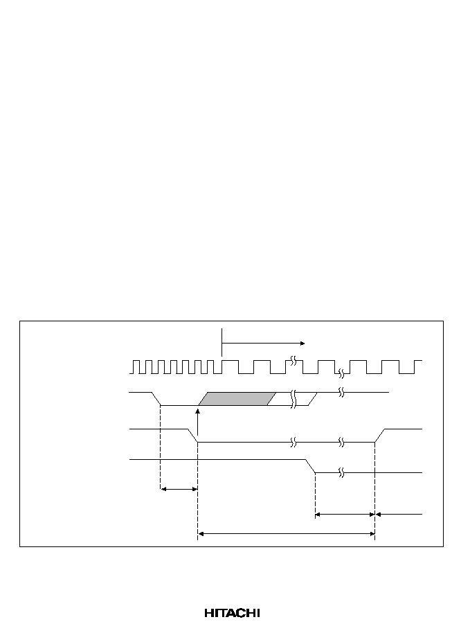
392
1. Set the TME bit in the watchdog timer's WTCSR register to 0.
2. Set the overflow time in bits CKS2 to CKS0 bits in the watchdog timer's WTCSR register
(overflow time should be calculated using the clock frequency after modification).
3. After the SLEEP instruction is executed and standby mode is entered, apply a low level from
the
CKPREQ/CKM pin.
4. When the chip is internally ready to modify the operating clock, a low level is output from the
CKPACK pin.
5. After the
CKPACK pin goes low, the clocks are stopped and the frequency is modified. The
internal chip state is the same as in standby mode.
6. When the clock pause state (standby) is canceled, the WDT starts to count up at the falling
edge or rising edge of the NMI pin (when the NMIE bit of INTC is set).
7. When a frequency is modified, the
CKPACK pin goes high after the time set by the WDT, and
the clock pause function gives external notification that the chip can again be operated
(standby mode is canceled).
8. When a clock is halted, the clock is applied again to the CKIO pin and NMI input is generated.
After the time set by the WDT, the
CKPACK pin goes high, and the clock pause function gives
external notification that the chip can again be operated (standby mode is canceled).
The standby state, all internal functions and all pin states during clock pause are equivalent to
those of the normal standby mode. Figure 14.2 shows the timing chart for the clock pause
function.
Clock frequency modification
CKIO input
CKPREQ
/CKM input
CKPACK
output
NMI input
Clock pause request cancellation
Standby time
WDT
setting time
NMI
exception
handling
Waiting for
clock pause
Figure 14.2 Clock Pause Function Timing

393
14.4.5
Notes on Standby Mode
1. When the SH7604 enters standby mode during use of the cache, disable the cache before
making the mode transition. Initialize the cache beforehand when the cache is used after
returning to standby mode. The contents of the on-chip RAM are not retained in standby mode
when cache is used as on-chip RAM.
2. If an on-chip peripheral register is written in the 10 clock cycles before the SH7604 transits to
standby mode, read the register before executing the SLEEP instruction.
3. When using clock mode 0, 1, or 2, the CKIO pin is the clock output pin. Note the following
when standby mode is used in these clock modes. When standby mode is canceled by NMI, an
unstable clock is output from the CKIO pin during the oscillation settling time after NMI input.
This also applies to clock output in the case of cancellation by a power-on reset or manual
reset. Power-on reset and manual reset input should be continued for a period at least equal to
for the oscillation settling time.
14.5
Module Standby Function
14.5.1
Transition to Module Standby Function
By setting one of standby control register bits MSTP4MSTP0 to 1, the supply of the clock to the
corresponding on-chip peripheral module can be halted. This function can be used to reduce the
power consumption in sleep mode. Do not perform read/write operations for a module in module
standby mode.
The external pins and registers of the DMAC, MULT, and DIVU on-chip peripheral modules
retain their states prior to halting. The external pins of the FRT and SCI are reset and all their
registers are initialized.
Do not switch on-chip peripheral modules to module standby mode while they are running.
14.5.2
Clearing the Module Standby Function
Clear the module standby function by clearing the MSTP4MSTP0 bits, or by a power-on reset or
manual reset.
To effect a module stop, halt the relevant module or disable interrupts.

394

395
Section 15 Electrical Characteristics (5V Version)
15.1
Absolute Maximum Ratings
Table 15.1 shows the absolute maximum ratings.
Table 15.1
Absolute Maximum Ratings
Item
Symbol
Rating
Unit
Power supply voltage
V
CC
0.3 to +7.0
V
Input voltage
Vin
0.3 to V
CC
+ 0.3
V
Operating temperature
Topr
20 to +75
°
C
Storage temperature
Tstg
55 to +125
°
C
Caution:
Operating the chip in excess of the absolute maximum rating may result in permanent
damage.

396
15.2
DC Characteristics
Tables 15.2 and 15.3 list DC characteristics.
Table 15.2
DC Characteristics (Conditions: V
CC
= 5.0 V
±
10%, Ta = 20 to +75
°
C)
Item
Symbol Min
Typ
Max
Unit Test Conditions
Input high-
RES
, NMI,
V
IH
V
CC
0.5 --
V
CC
+ 0.3 V
During standby
level
MD5MD0
V
CC
0.7 --
V
CC
+ 0.3 V
Normal operation
voltage
EXTAL, CKIO
V
CC
0.7 --
V
CC
+ 0.3 V
Other input pins
2.2
--
V
CC
+ 0.3 V
Input low-
RES
, NMI,
V
IL
0.3
--
0.5
V
During standby
level
MD5MD0
0.3
--
0.8
V
Normal operation
voltage
Other input pins
0.3
--
0.8
V
Input leak
RES
|Iin|
--
--
1.0
µ
A
Vin = 0.5 to V
CC
0.5 V
current
NMI, MD5MD0
--
--
1.0
µ
A
Vin = 0.5 to V
CC
0.5 V
Other input pins
--
--
1.0
µ
A
Vin = 0.5 to V
CC
0.5 V
3-state
leak
current
(while off)
A26A0, D31
D0,
BS
,
CS3
CS0
, RD/
WR
,
RAS
,
CAS
,
WE3
WE0
,
RD
,
IVECF
|I
STI
|
--
--
1.0
µ
A
Vin = 0.5 to V
CC
0.5 V
Output
All output pins
V
OH
V
CC
0.5 --
--
V
I
OH
= 200
µ
A
high-level
voltage
3.5
--
--
V
I
OH
= 1 mA
Output
low-level
voltage
All output pins
V
OL
--
--
0.4
V
I
OL
= 1.6 mA
Input
RES
Cin
--
--
15
pF
Vin = 0 V
capaci-
NMI
--
--
15
pF
f = 1 MHz
tance
All other input
pins (including
D31D0)
--
--
15
pF
Ta = 25
°
C

397
Table 15.2
DC Characteristics (Conditions: V
CC
= 5.0 V
±
10%, Ta = 20 to +75
°
C) (cont)
Item
Symbol Min
Typ
Max
Unit Test Conditions
Current
Normal
I
CC
--
60
80
mA
f = 8 MHz
consump-
operation
--
80
100
mA
f = 16 MHz
tion
--
110
160
mA
f = 28.7 MHz
Sleep
--
30
55
mA
f = 8 MHz
--
50
70
mA
f = 16 MHz
--
80
100
mA
f = 28.7 MHz
Standby
--
1
15
µ
A
Ta
50
°
C
--
--
60
µ
A
50
°
C < Ta
Notes: 1. When no PLL is used, do not leave the PLLV
CC
and PLLV
SS
pins open. Connect
PLLV
CC
to V
CC
and PLLV
SS
to V
SS
.
2. Current consumption values shown are the values at which all output pins are without
load under conditions of V
IH
min = V
CC
0.5 V, V
IL
max = 0.5 V.
Table 15.3
Permitted Output Current Values (Conditions: V
CC
= 5.0 V
±
10%, Ta = 20 to
+75
°
C)
Item
Symbol
Min
Typ
Max
Unit
Output low-level permissible current (per pin)
I
OL
--
--
2.0
mA
Output low-level permissible current (total)
I
OL
--
--
80
mA
Output high-level permissible current (per pin)
I
OH
--
--
2.0
mA
Output high-level permissible current (total)
(I
OH
)
--
--
25
mA
Caution:
To ensure chip reliability, do not exceed the output current values given in table 15.3.
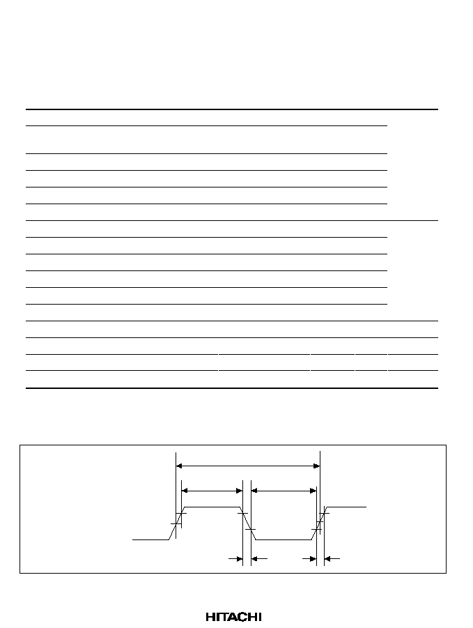
398
15.3
AC Characteristics
15.3.1
Clock Timing
Table 15.4
Clock Timing (Conditions: V
CC
= 5.0 V
±
10%, Ta = 20 to +75
°
C)
Item
Symbol
Min
Max
Unit
Figures
Operating frequency
f
OP
4
28.7
MHz
15.1
Clock cycle time
t
cyc
35
143
*1
or
250
*2
ns
Clock high pulse width
t
CH
8
*1
or 15
*2
--
ns
Clock low pulse width
t
CL
8
*1
or 15
*2
--
ns
Clock rise time
t
CR
--
5
ns
Clock fall time
t
CF
--
5
ns
EXTAL clock input frequency
f
EX
4
8
MHz
15.2
EXTAL clock input cycle time
t
EXcyc
125
250
ns
EXTAL clock input low-level pulse width
t
EXL
50
--
ns
EXTAL clock input high-level pulse width
t
EXH
50
--
ns
EXTAL clock input rise time
t
EXR
--
5
ns
EXTAL clock input clock fall time
t
EXF
--
5
ns
Power-on oscillation settling time
t
OSC1
10
--
ms
15.3
Software standby oscillation settling time 1
t
OSC2
10
--
ms
15.4
Software standby oscillation settling time 2
t
OSC3
10
--
ms
15.5
PLL synchronization settling time
t
PLL
1
--
µ
s
15.6
Notes: 1. With PLL circuit 1 operating.
2. With PLL circuit 1 not used.
t
CH
1/2 V
CC
t
CF
t
CR
1/2 V
CC
V
IH
CKIO
(input)
V
IH
V
IH
V
IL
V
IL
t
CL
t
cyc
Figure 15.1 CKIO Input Timing
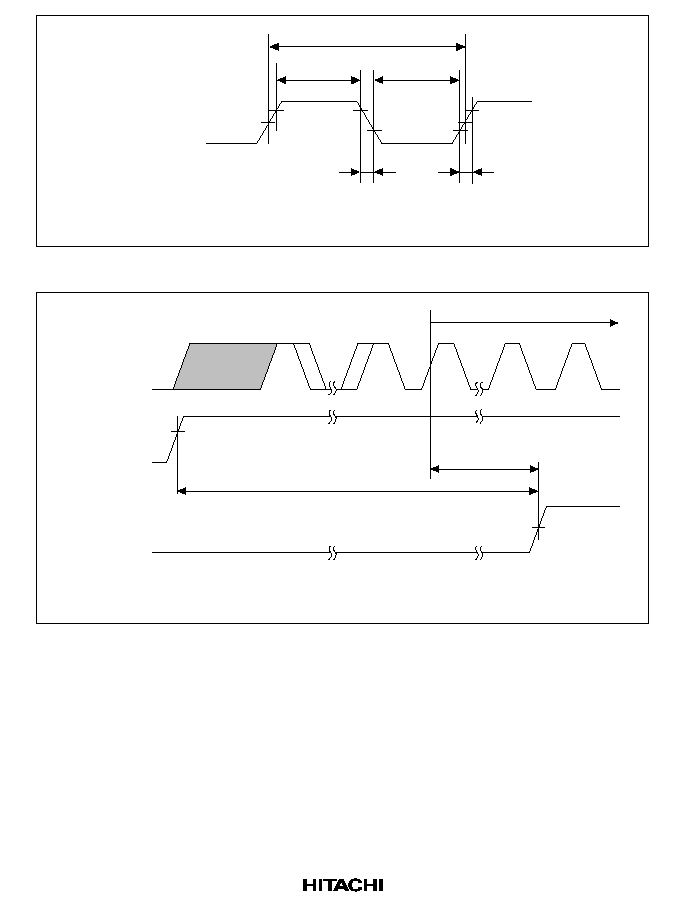
399
EXTAL
(input)
1/2 V
CC
t
EXcyc
t
EXL
t
EXH
t
EXF
t
EXR
V
IH
V
IH
V
IL
V
IL
V
IH
1/2 V
CC
Note:
External clock input from EXTAL pin.
Figure 15.2 EXTAL Clock Input Timing
CKIO,
internal clock
V
CC
V
CC
min
RES
t
OSC1
t
RESW
Stable oscillation
Note:
Oscillation settling time when on-chip crystal oscillator is used.
Figure 15.3 Oscillation Settling Time at Power-On

400
CKIO,
internal
clock
Stable oscillation
Standby
period
t
OSC2
t
RESW
RES
Note:
Oscillation settling time when on-chip crystal oscillator is used.
Figure 15.4 Oscillation Settling Time at Standby Return (via
RES)
CKIO,
internal
clock
Stable oscillation
Standby
period
t
OSC3
NMI
Note:
Oscillation settling time when on-chip crystal oscillator is used.
Figure 15.5 Oscillation Settling Time at Standby Return (via NMI)
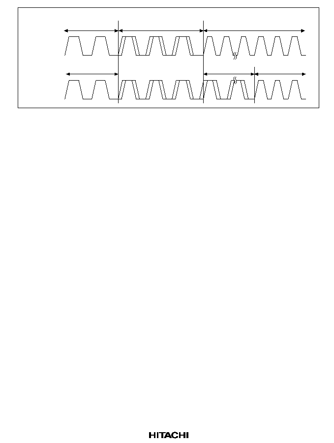
401
Stable
oscillation
Stable
oscillation
Oscillation frequency
modification
t
PLL
PLL
synchronization
PLL
synchronization
EXTAL
or CKIO
Internal
clock
Figure 15.6 PLL Synchronization Settling Time

402
15.3.2
Control Signal Timing
Table 15.5
Control Signal Timing (Conditions: V
CC
= 5.0 V
±
10%, Ta = 20 to +75
°
C)
Item
Symbol Min
Max
Unit
Figure
RES
rise, fall
t
RESr
,
t
RESf
--
200
ns
15.7
RES
pulse width
t
RESW
20
--
t
cyc
NMI reset setup time
t
NMIRS
tcyc + 10
--
ns
NMI reset hold time
t
NMIRH
tcyc + 10
--
ns
NMI rise, fall
t
NMIr
,
t
NMIf
--
200
ns
NMI minimum pulse width
t
IRQES
3
--
tcyc
RES
setup time
*
t
RESS
30
--
ns
15.8,
NMI setup time
*
t
NMIS
30
--
ns
15.9
IRL3
IRL0
setup time
*
t
IRLS
30
--
ns
RES
hold time
t
RESH
10
--
ns
15.8,
NMI hold time
t
NMIH
10
--
ns
15.9
IRL3
IRL0
hold time
t
IRLH
10
--
ns
BRLS
setup time 1 (PLL on)
t
BLSS1
1/2 tcyc + 9 --
ns
15.10
BRLS
hold time 1 (PLL on)
t
BLSH1
9 1/2 tcyc --
ns
BGR
delay time 1 (PLL on)
t
BGRD1
--
1/2 tcyc + 18 ns
BRLS
setup time 1 (PLL on, 1/4 cycle delay)
t
BLSS1
1/4 tcyc + 9 --
ns
15.10
BRLS
hold time 1 (PLL on, 1/4 cycle delay)
t
BLSH1
9 1/4 tcyc --
ns
BGR
delay time 1 (PLL on, 1/4 cycle delay)
t
BGRD1
--
3/4 tcyc + 18 ns
BRLS
setup time 2 (PLL off)
t
BLSS2
9
--
ns
15.11
BRLS
hold time 2 (PLL off)
t
BLSH2
19
--
ns
BGR
delay time 2 (PLL off)
t
BGRD2
--
28
ns
Note:
The
RES
, NMI and
IRL3
-
IRL0
signals are asynchronous inputs, but when the setup times
shown here are observed, the signals are considered to have changed at clock fall. If the
setup times are not observed, recognition may be delayed until the next clock fall.

403
Table 15.5
Control Signal Timing (Conditions: V
CC
= 5.0 V
±
10%, Ta = 20 to +75
°
C)
(cont)
Item
Symbol Min
Max
Unit
Figure
BREQ
delay time 1 (PLL on)
t
BRQD1
--
1/2 tcyc + 18 ns
15.12
BACK
setup time 1 (PLL on)
t
BAKS1
1/2 tcyc + 9 --
ns
BACK
hold time 1 (PLL on)
t
BAKH1
9 1/2 tcyc --
ns
BREQ
delay time 1 (PLL on, 1/4 cycle delay)
t
BRQD1
--
3/4 tcyc + 18 ns
15.12
BACK
setup time 1 (PLL on, 1/4 cycle delay)
t
BAKS1
1/4 tcyc + 9 --
ns
BACK
hold time 1 (PLL on, 1/4 cycle delay)
t
BAKH1
9 1/4 tcyc --
ns
BREQ
delay time 2 (PLL off)
t
BRQD2
--
28
ns
15.13
BACK
setup time 2 (PLL off)
t
BAKS2
9
--
ns
BACK
hold time 2 (PLL off)
t
BAKH2
19
--
ns
Bus tri-state delay time 1 (PLL on)
t
BOFF1
0
25
ns
15.10,
Bus buffer on time 1 (PLL on)
t
BON1
0
18
ns
15.12
Bus tri-state delay time 1 (PLL on, 1/4 cycle
delay)
t
BOFF1
1/4 tcyc
1/4 tcyc + 25 ns
15.10,
15.12
Bus buffer on time 1 (PLL on, 1/4 cycle delay) t
BON1
1/4 tcyc
1/4 tcyc + 18 ns
Bus tri-state delay time 1 (PLL off)
t
BOFF1
0
30
ns
15.11,
Bus buffer on time 1 (PLL off)
t
BON1
0
25
ns
15.13
Bus tri-state delay time 2 (PLL on)
t
BOFF2
1/2 tcyc
1/2 tcyc + 25 ns
15.10,
Bus buffer on time 2 (PLL on)
t
BON2
1/2 tcyc
1/2 tcyc + 18 ns
15.12
Bus tri-state delay time 2 (PLL on, 1/4 cycle
delay)
t
BOFF2
3/4 tcyc
3/4 tcyc + 25 ns
15.10,
Bus buffer on time 2 (PLL on, 1/4 cycle delay) t
BON2
3/4 tcyc
3/4 tcyc + 18 ns
15.12
Bus tri-state delay time 3 (PLL off)
t
BOFF3
0
30
ns
15.11,
Bus buffer on time 3 (PLL off)
t
BON3
0
25
ns
15.13
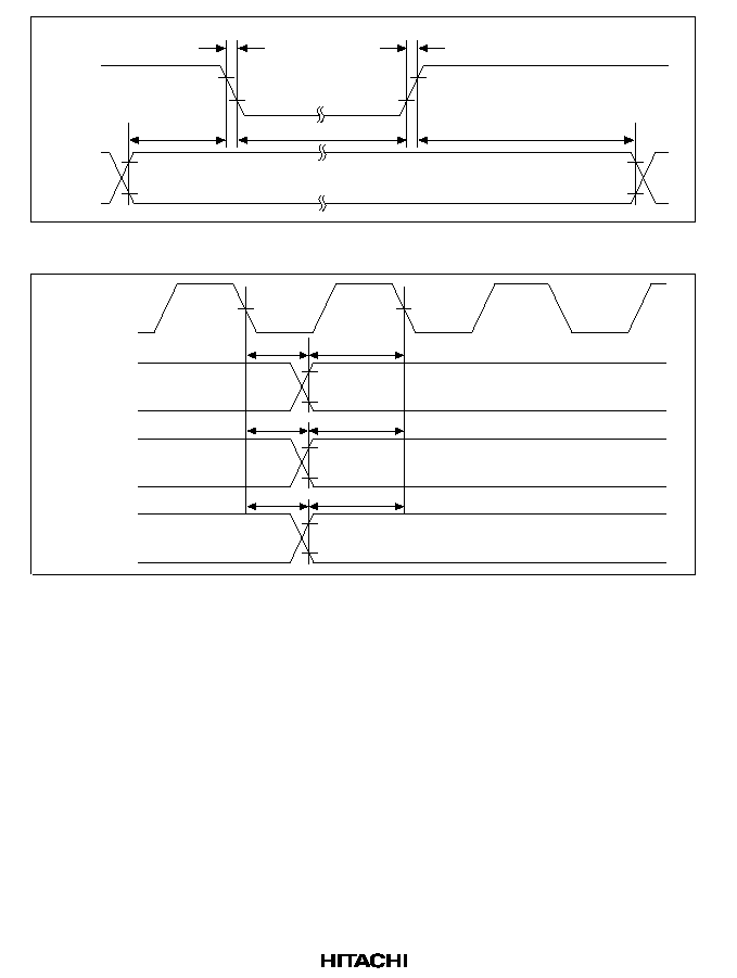
404
t
NMIRS
t
RESW
t
RESf
t
RESr
t
NMIRH
RES
NMI
V
IH
V
IL
V
IH
V
IL
V
IH
V
IL
V
IH
V
IL
Figure 15.7 Reset Input Timing
t
RESS
CKIO
RES
t
INMIS
NMI
t
IRLS
IRL3
IRL0
t
RESH
t
NMIH
t
IRLH
V
IH
V
IL
V
IH
V
IL
V
IH
V
IL
Figure 15.8 Interrupt Signal Input Timing (With PLL1 Off)
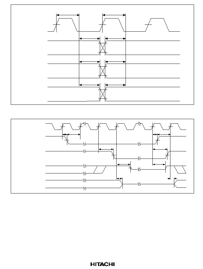
405
CKIO
RES
t
RESH
t
RESS
V
IH
V
IL
NMI
t
NMIH
t
NMIS
V
IH
V
IL
IRL3
IRL0
t
IRLH
t
IRLS
V
IH
V
IL
1/2 t
cyc
or 3/4 t
cyc
1/2 t
cyc
or 3/4 t
cyc
Figure 15.9 Interrupt Signal Input Timing (PLL1 On)
t
BLSS1
CKIO
BRLS
(input)
BGR
(output)
RD
, RD/
WR
,
RAS
,
CAS
,
CSn
,
WEn
,
BS
,
IVECF
A26A0
D31D0
t
BOFF2
t
BOFF1
t
BLSH1
t
BGRD1
t
BLSS1
t
BLSH1
t
BON2
t
BON1
t
BGRD1
Figure 15.10 Bus Release Timing (Master Mode, PLL1 On)
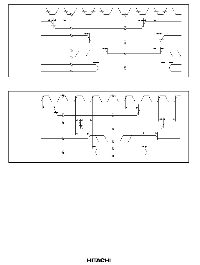
406
A26A0
D31D0
RD
, RD/
WR
,
RAS
,
CAS
,
CSn
,
WEn
,
BS
,
IVECF
BRLS
(input)
BGR
(output)
t
BLSS2
CKIO
t
BOFF1
t
BON1
t
BON3
t
BOFF3
t
BGRD2
t
BGRD2
t
BLSH2
t
BLSS2
t
BLSH2
Figure 15.11 Bus Release Timing (Master Mode, PLL1 Off)
BACK
(input)
RD
, RD/
WR
,
RAS
,
CAS
,
CSn
,
WEn
,
BS
,
IVECF
A26A0
D31D0
BREQ
(output)
t
BAKH1
CKIO
t
BRQD1
t
BRQD1
t
BAKH1
t
BAKS1
t
BON2
t
BON1
t
BOFF1
t
BOFF2
t
BAKS1
Figure 15.12 Bus Release Timing (Slave Mode, PLL1 On)
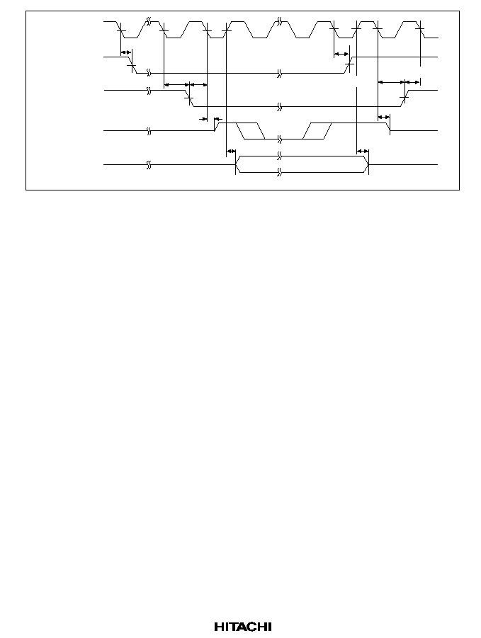
407
BACK
(input)
RD
, RD/
WR
,
RAS
,
CAS
,
CSn
,
WEn
,
BS
,
IVECF
A26A0
D31D0
BREQ
(output)
CKIO
t
BRQD2
t
BRQD1
t
BAKH2
t
BAKS2
t
BON3
t
BON1
t
BOFF1
t
BOFF3
t
BAKH2
t
BAKS2
Figure 15.13 Bus Release Timing (Slave Mode, PLL1 Off)

408
15.3.3
Bus Timing
Table 15.6
Bus Timing With PLL On [Mode 0, 4] (Conditions: V
CC
= 5.0 V
±
10%,
Ta = 20 to +75
°
C)
Item
Symbol
Min
Max
Unit
Figures
Address delay time
t
AD
3
18
ns
15.14, 15.20, 15.40,
15.52, 15.66, 15.68
BS
delay time
t
BSD
--
21
ns
15.14, 15.20, 15.40,
15.52, 15.66
CS
delay time 1
t
CSD1
--
21
ns
15.14, 15.20, 15.40,
15.52, 15.66
CS
delay time 2
t
CSD2
--
1/2 tcyc + 21 ns
15.14, 15.66
Read/write delay time
t
RWD
3
18
ns
15.14, 15.20, 15.40,
15.52, 15.66
Read strobe delay time 1
t
RSD1
--
1/2 tcyc + 16 ns
15.14, 15.40, 15.52,
15.66, 15.68
Read data setup time 1
t
RDS1
1/2 tcyc + 10 --
ns
15.14, 15.40, 15.52,
15.66, 15.68
Read data setup time 3
(SDRAM)
t
RDS3
1/2 tcyc + 8
--
ns
15.20
Read data hold time 2
t
RDH2
0
--
ns
15.14, 15.66
Read data hold time 4
(SDRAM)
t
RDH4
0
--
ns
15.20
Read data hold time 5
(DRAM)
t
RDH5
0
--
ns
15.40
Read data hold time 6
(PSRAM)
t
RDH6
0
--
ns
15.52
Read data hold time 7
(interrupt vector)
t
RDH7
0
--
ns
15.68
Write enable delay time
t
WED1
1/2 tcyc + 3
1/2 tcyc + 18 ns
15.14, 15.15, 15.52,
15.53
Write data delay time 1
t
WDD
3
18
ns
15.15, 15.27, 15.41,
15.53
Write data hold time 1
t
WDH1
3
--
ns
15.15, 15.27, 15.41,
15.53
Data buffer on time
t
DON
--
18
ns
15.15, 15.27, 15.41,
15.53
Data buffer off time
t
DOF
--
18
ns
15.15, 15.27, 15.41,
15.53

409
Table 15.6
Bus Timing With PLL On [Mode 0, 4] (cont)
(Conditions: V
CC
= 5.0 V
±
10%, Ta = 20 to +75
°
C)
Item
Symbol
Min
Max
Unit
Figures
DACK delay time 1
t
DACD1
--
18
ns
15.14, 15.20, 15.40,
15.52, 15.66
DACK delay time 2
t
DACD2
--
1/2 tcyc + 18 ns
15.14, 15.20, 15.40,
15.52, 15.66
WAIT
setup time
t
WTS
20
--
ns
15.19, 15.43, 15.55,
15.66, 15.70
WAIT
hold time
t
WTH
5
--
ns
15.19, 15.43, 15.55,
15.66, 15.70
RAS
delay time 1 (SDRAM) t
RASD1
--
18
ns
15.20
RAS
delay time 2 (DRAM)
t
RASD2
1/2 tcyc + 3
1/2 tcyc + 18 ns
15.40
CAS
delay time 1 (SDRAM) t
CASD1
--
18
ns
15.20
CAS
delay time 2 (DRAM)
t
CASD2
1/2 tcyc + 3
1/2 tcyc + 18 ns
15.40
DQM delay time
t
DQMD
--
18
ns
15.20
CKE delay time
t
CKED
--
21
ns
15.37
CE
delay time 1
t
CED1
1/2 tcyc + 3
1/2 tcyc + 18 ns
15.52
OE
delay time 1
t
OED1
--
1/2 tcyc + 18 ns
15.52
IVECF
delay time
t
IVD
--
18
ns
15.68
Address input setup time
t
ASIN
14
--
ns
15.71
Address input hold time
t
AHIN
3
--
ns
15.71
BS
input setup time
t
BSS
15
--
ns
15.71
BS
input hold time
t
BSH
3
--
ns
15.71
Read/write input setup time
t
RWS
15
--
ns
15.71
Read/write input hold time
t
RWH
3
--
ns
15.71
Address hold time 1
t
AH1
5
--
ns
15.15

410
Table 15.7
Bus Timing With PLL On and 1/4 Cycle Delay [Mode 1, 5]
(Conditions: V
CC
= 5.0 V
±
10%, Ta = 20 to +75
°
C)
Item
Symbol
Min
Max
Unit
Figures
Address delay time
t
AD
1/4 tcyc + 3
1/4 tcyc + 18 ns
15.14, 15.20, 15.40,
15.52, 15.66, 15.68
BS
delay time
t
BSD
--
1/4 tcyc + 21 ns
15.14, 15.20, 15.40,
15.52, 15.66
CS
delay time 1
t
CSD1
--
1/4 tcyc + 21 ns
15.14, 15.20, 15.40,
15.52, 15.66
CS
delay time 2
t
CSD2
--
3/4 tcyc + 21 ns
15.14, 15.66
Read/write delay time
t
RWD
1/4 tcyc + 3
1/4 tcyc + 18 ns
15.14, 15.20, 15.40,
15.52, 15.66
Read strobe delay time 1
t
RSD1
--
3/4 tcyc + 16 ns
15.14, 15.40, 15.52,
15.66, 15.68
Read data setup time 1
t
RDS1
1/4 tcyc + 10 --
ns
15.14, 15.40, 15.52,
15.66, 15.68
Read data setup time 3
(SDRAM)
t
RDS3
1/4 tcyc + 8
--
ns
15.20
Read data hold time 2
t
RDH2
0
--
ns
15.14, 15.66
Read data hold time 4
(SDRAM)
t
RDH4
0
--
ns
15.20
Read data hold time 5
(DRAM)
t
RDH5
0
--
ns
15.40
Read data hold time 6
(PSRAM)
t
RDH6
0
--
ns
15.52
Read data hold time 7
(interrupt vector)
t
RDH7
0
--
ns
15.68
Write enable delay time
t
WED1
3/4 tcyc + 3
3/4 tcyc + 18 ns
15.14, 15.15, 15.52,
15.53
Write data delay time 1
t
WDD
1/4 tcyc + 3
1/4 tcyc + 18 ns
15.15, 15.27, 15.41,
15.53
Write data hold time 1
t
WDH1
1/4 tcyc + 3
--
ns
15.15, 15.27, 15.41,
15.53
Data buffer on time
t
DON
--
1/4 tcyc + 18 ns
15.15, 15.27, 15.41,
15.53
Data buffer off time
t
DOF
--
1/4 tcyc + 18 ns
15.15, 15.27, 15.41,
15.53

411
Table 15.7
Bus Timing With PLL On and 1/4 Cycle Delay [Mode 1, 5] (cont)
(Conditions: V
CC
= 5.0 V
±
10%, Ta = 20 to +75
°
C)
Item
Symbol
Min
Max
Unit
Figures
DACK delay time 1
t
DACD1
--
1/4 tcyc + 18 ns
15.14, 15.20, 15.40,
15.52, 15.66
DACK delay time 2
t
DACD2
--
3/4 tcyc + 18 ns
15.14, 15.20, 15.40,
15.52, 15.66
WAIT
setup time
t
WTS
20 1/4 tcyc --
ns
15.19, 15.43, 15.55,
15.66, 15.70
WAIT
hold time
t
WTH
1/4 tcyc + 5
--
ns
15.19, 15.43, 15.55,
15.66, 15.70
RAS
delay time 1 (SDRAM) t
RASD1
--
1/4 tcyc + 18 ns
15.20
RAS
delay time 2 (DRAM)
t
RASD2
3/4 tcyc + 3
3/4 tcyc + 18 ns
15.40
CAS
delay time 1 (SDRAM) t
CASD1
--
1/4 tcyc + 18 ns
15.20
CAS
delay time 2 (DRAM)
t
CASD2
3/4 tcyc + 3
3/4 tcyc + 18 ns
15.40
DQM delay time
t
DQMD
--
1/4 tcyc + 18 ns
15.20
CKE delay time
t
CKED
--
1/4 tcyc + 21 ns
15.37
CE
delay time 1
t
CED1
3/4 tcyc + 3
3/4 tcyc + 18 ns
15.52
OE
delay time 1
t
OED1
--
3/4 tcyc + 18 ns
15.52
IVECF
delay time
t
IVD
--
1/4 tcyc + 18 ns
15.68
Address input setup time
t
ASIN
14 1/4 tcyc --
ns
15.71
Address input hold time
t
AHIN
1/4 tcyc + 3
--
ns
15.71
BS
input setup time
t
BSS
15 1/4 tcyc --
ns
15.71
BS
input hold time
t
BSH
1/4 tcyc + 3
--
ns
15.71
Read/write input setup time t
RWS
15 1/4 tcyc --
ns
15.71
Read/write input hold time
t
RWH
1/4 tcyc + 3
--
ns
15.71
Address hold time 1
t
AH1
5
--
ns
15.15

412
Table 15.8
Bus Timing With PLL Off (CKIO Input) [Mode 6]
(Conditions: V
CC
= 5.0 V
±
10%, Ta = 20 to +75
°
C)
Item
Symbol
Min
Max
Unit
Figures
Address delay time
t
AD
13
28
ns
15.16, 15.38, 15.47,
15.60, 15.67, 15.69
BS
delay time
t
BSD
--
30
ns
15.16, 15.38, 15.47,
15.60, 15.67
CS
delay time 1
t
CSD1
--
30
ns
15.16, 15.38, 15.47,
15.60, 15.67
CS
delay time 3
t
CSD3
--
28
ns
15.16, 15.67
Read write delay time
t
RWD
13
28
ns
15.16, 15.38, 15.47,
15.60, 15.67
Read strobe delay time 2
t
RSD2
--
26
ns
15.16, 15.47, 15.60,
15.67, 15.69
Read data setup time 2
t
RDS2
10
--
ns
15.16, 15.38, 15.47,
15.60, 15.67, 15.69
Read data hold time 2
t
RDH2
0
--
ns
15.16, 15.67
Read data hold time 3
t
RDH3
15
--
ns
15.38
Read data hold time 5
(DRAM)
t
RDH5
0
--
ns
15.47
Read data hold time 6
(PSRAM)
t
RDH6
0
--
ns
15.60
Read data hold time 7
(interrupt vector)
t
RDH7
0
--
ns
15.69
Write enable delay time 2
t
WED2
10
25
ns
15.17, 15.61
Write data delay time
t
WDD
10
25
ns
15.17, 15.39, 15.48,
15.61
Write data hold time 1
t
WDH1
3
ns
15.17, 15.39, 15.48,
15.61
Write data hold time 2
t
WDH2
5
ns
15.17
Write data hold time 3
t
WDH3
3
ns
15.61
DACK delay time 1
t
DACD1
--
25
ns
15.16, 15.38, 15.47,
15.60, 15.67
DACK delay time 3
t
DACD3
--
25
ns
15.16, 15.38, 15.47,
15.60, 15.67

413
Table 15.8
Bus Timing With PLL Off (CKIO Input) [Mode 6] (cont)
(Conditions: V
CC
= 5.0 V
±
10%, Ta = 20 to +75
°
C)
Item
Symbol
Min
Max
Unit
Figures
WAIT
setup time
t
WTS
20
--
ns
15.19, 15.43, 15.55,
15.67, 15.70
WAIT
hold time
t
WTH
15
--
ns
15.19, 15.43, 15.55,
15.67, 15.70
RAS
delay time 1 (SDRAM) t
RASD1
--
25
ns
15.38
RAS
delay time 3 (DRAM)
t
RASD3
10
25
ns
15.47
CAS
delay time 1 (SDRAM) t
CASD1
--
25
ns
15.38
CAS
delay time 3 (DRAM)
t
CASD3
10
25
ns
15.47
DQM delay time
t
DQMD
--
25
ns
15.38
CKE delay time
t
CKED
--
25
ns
15.37
CE
delay time 2
t
CED2
10
25
ns
15.60
OE
delay time 2
t
OED2
--
25
ns
15.60
IVECF
delay time
t
IVD
--
25
ns
15.69
WE
setup time
t
WES1
0
--
ns
15.16
Address setup time 1
t
AS1
0
--
ns
15.17
Address setup time 2
t
AS2
3
--
ns
15.60
Address hold time 2
t
AH2
0
--
ns
15.17
Row address setup time
t
ASR
3
--
ns
15.47
Column address setup time t
ASC
3
--
ns
15.47
Write command setup time
t
WCS
3
--
ns
15.48
Write data setup time
t
WDS
3
--
ns
15.48
Address input setup time
*
t
ASIN
15
--
ns
15.71
Address input hold time
*
t
AHIN
10
--
ns
15.71
BS
input setup time
*
t
BSS
15
--
ns
15.71
BS
input hold time
*
t
BSH
10
--
ns
15.71
Read/write input setup time
*
t
RWS
15
--
ns
15.71
Read/write input hold time
*
t
RWH
10
--
ns
15.71
Data buffer on time
t
DON
--
25
ns
15.17, 15.39, 15.48,
15.61
Data buffer off time
t
DOF
--
25
ns
15.17, 15.39, 15.48,
15.61
Note:
When the external addresses monitor function is used, the PLL must be on.

414
Table 15.9
Bus Timing With PLL Off (CKIO Output) [Mode 2]
(Conditions: V
CC
= 5.0 V
±
10%, Ta = 20 to +75
°
C)
Item
Symbol
Min
Max
Unit
Figures
Address delay time
t
AD
3
18
ns
15.16, 15.38, 15.47,
15.60, 15.67, 15.69
BS
delay time
t
BSD
--
21
ns
15.16, 15.38, 15.47,
15.60, 15.67
CS
delay time 1
t
CSD1
--
21
ns
15.16, 15.38, 15.47,
15.60, 15.67
CS
delay time 3
t
CSD3
--
21
ns
15.16, 15.67
Read write delay time
t
RWD
3
18
ns
15.16, 15.38, 15.47,
15.60, 15.67
Read strobe delay time 2
t
RSD2
--
16
ns
15.16, 15.47, 15.60,
15.67, 15.69
Read data setup time 2
t
RDS2
12
--
ns
15.16, 15.38, 15.47,
15.60, 15.67, 15.69
Read data hold time 2
t
RDH2
0
--
ns
15.16, 15.67
Read data hold time 3
(SDRAM)
t
RDH3
1/2 tcyc
--
ns
15.38
Read data hold time 5
(DRAM)
t
RDH5
0
--
ns
15.47
Read data hold time 6
(PSRAM)
t
RDH6
0
--
ns
15.60
Read data hold time 7
(interrupt vector)
t
RDH7
0
--
ns
15.69
Write enable delay time 2
t
WED2
3
18
ns
15.17, 15.61
Write data delay time
t
WDD
3
18
ns
15.17, 15.39, 15.48,
15.61
Write data hold time 1
t
WDH1
3
--
ns
15.17, 15.39, 15.48,
15.61
Write data hold time 2
t
WDH2
5
--
ns
15.17
Write data hold time 3
t
WDH3
3
--
ns
15.61
DACK delay time 1
t
DACD1
--
18
ns
15.16, 15.38, 15.47,
15.60, 15.67
DACK delay time 3
t
DACD3
--
18
ns
15.16, 15.38, 15.47,
15.60, 15.67

415
Table 15.9
Bus Timing With PLL Off (CKIO Output) [Mode 2] (cont)
(Conditions: V
CC
= 5.0 V
±
10%, Ta = 20 to +75
°
C)
Item
Symbol
Min
Max
Unit
Figures
WAIT
setup time
t
WTS
22
--
ns
15.19, 15.43, 15.55,
15.67, 15.70
WAIT
hold time
t
WTH
5
--
ns
15.19, 15.43, 15.55,
15.67, 15.70
RAS
delay time 1 (SDRAM) t
RASD1
--
18
ns
15.38
RAS
delay time 3 (DRAM)
t
RASD3
3
18
ns
15.47
CAS
delay time 1 (SDRAM) t
CASD1
--
18
ns
15.38
CAS
delay time 3 (DRAM)
t
CASD3
3
18
ns
15.47
DQM delay time
t
DQMD
--
18
ns
15.38
CKE delay time
t
CKED
--
21
ns
15.37
CE
delay time 2
t
CED2
3
18
ns
15.60
OE
delay time 2
t
OED2
--
18
ns
15.60
IVECF
delay time
t
IVD
--
18
ns
15.69
Address input setup time
*
t
ASIN
14
--
ns
15.71
Address input hold time
*
t
AHIN
3
--
ns
15.71
BS
input setup time
*
t
BSS
15
--
ns
15.71
BS
input hold time
*
t
BSH
3
--
ns
15.71
Read/write input setup time
*
t
RWS
15
--
ns
15.71
Read/write input hold time
*
t
RWH
3
--
ns
15.71
Data buffer on time
t
DON
--
18
ns
15.17, 15.39, 15.48,
15.61
Data buffer off time
t
DOF
--
18
ns
15.17, 15.39, 15.48,
15.61
Address hold time 2
t
AH2
5
--
ns
15.17
Note:
When the external addresses monitor function is used, the PLL must be on.

416
CKIO
BS
CSn
RD/
WR
,
WE
RD
WEn
,
CASxx
,
DQMxx
RAS
,
CE
CAS
,
OE
CKE
D31D0
DACKn
WAIT
A26A0
T
1
T
2
t
AD
t
BSD
t
BSD
t
AD
t
CSD1
t
RWD
t
RWD
t
WED1
t
RDS1
t
RDH2
t
WED1
t
CSD2
t
RSD1
t
RSD1
t
DACD1
t
DACD2
Notes: 1.
2.
3.
The dotted line shows the waveform when synchronous DRAM is connected.
t
RDH2
is specified from the rise of
CSn
or
RD
, whichever is first.
The DACKn waveform shown is for the case where active-high has been specified.
Figure 15.14 Basic Read Cycle (No Waits, PLL On)
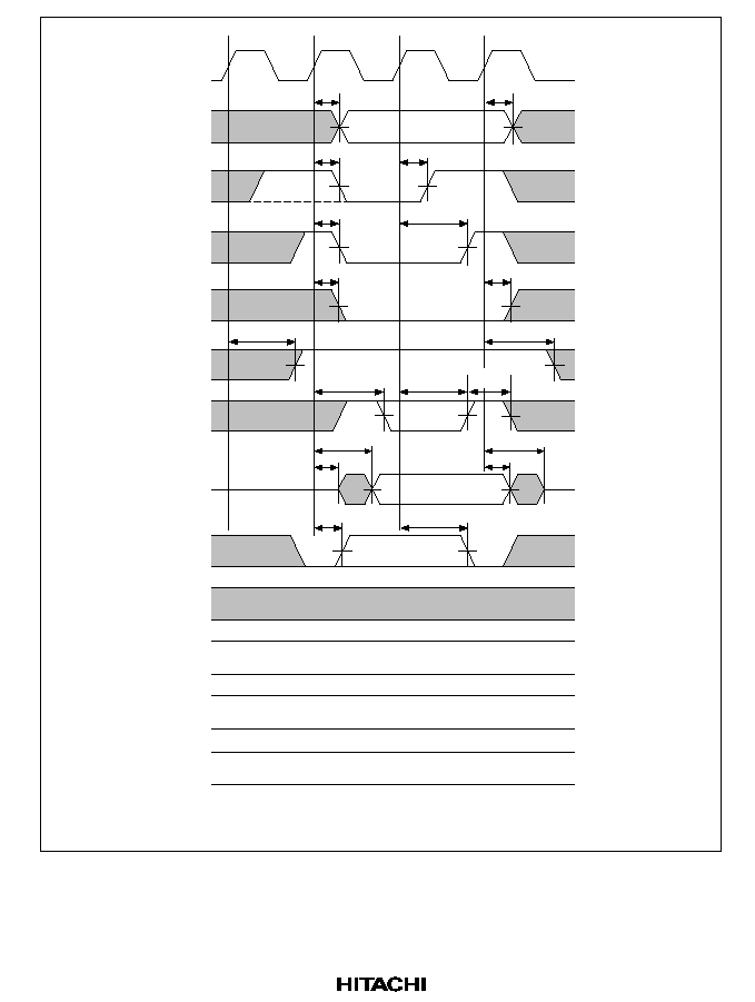
417
CKIO
BS
CSn
RD/
WR
,
WE
RD
WEn
,
CASxx
,
DQMxx
RAS
,
CE
CAS
,
OE
CKE
D31D0
DACKn
WAIT
A26A0
T
1
T
2
t
AD
t
BSD
t
BSD
t
AD
t
CSD1
t
RWD
t
RWD
t
RSD1
t
RSD1
t
CSD2
t
WED1
t
WED1
t
AH1
t
DACD1
t
DACD2
t
DON
t
WDH1
t
WDD
t
DOF
Notes: 1.
2.
The dotted line shows the waveform when synchronous DRAM is connected.
The DACKn waveform shown is for the case where active-high has been
specified.
Figure 15.15 Basic Write Cycle (No Waits, PLL On)
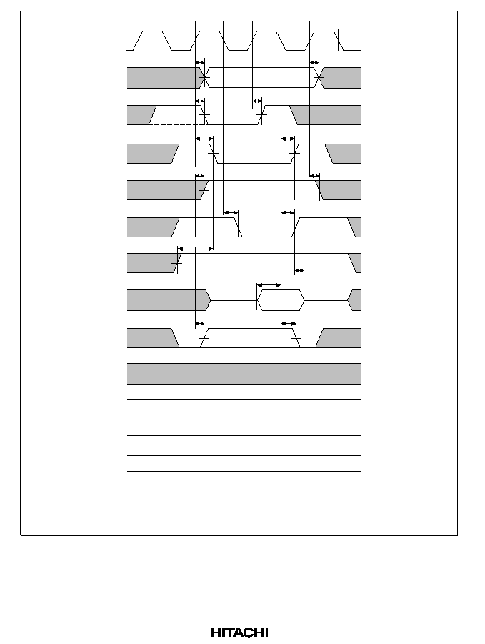
418
CKIO
BS
CSn
RD/
WR
,
WE
RD
WEn
,
CASxx
,
DQMxx
RAS
,
CE
CAS
,
OE
CKE
D31D0
DACKn
WAIT
A26A0
T
1
T
2
t
AD
t
BSD
t
BSD
t
AD
t
CSD1
t
RWD
t
RDS2
t
RDH2
t
CSD3
t
RSD2
t
DACD1
t
DACD3
t
RWD
t
RSD2
t
WES1
Notes: 1.
2.
3.
The dotted line shows the waveform when synchronous DRAM is connected.
t
RDH2
is specified from the rise of
CSn
or
RD
, whichever is first.
The DACKn waveform shown is for the case where active-high has been specified.
Figure 15.16 Basic Read Cycle (No Waits, PLL Off)
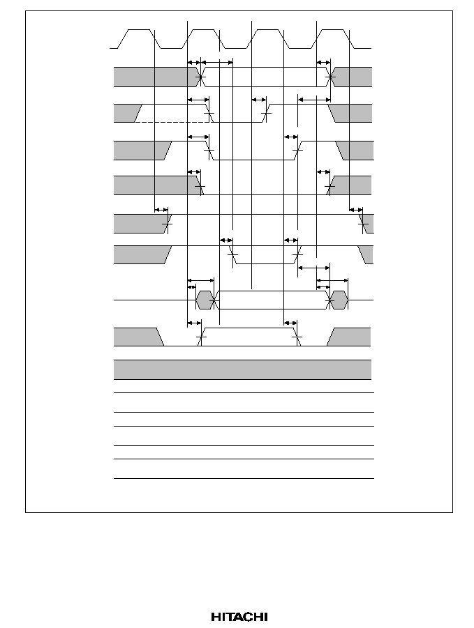
419
CKIO
BS
CSn
RD/
WR
,
WE
RD
WEn
,
CASxx
,
DQMxx
RAS
,
CE
CAS
,
OE
CKE
D31D0
DACKn
WAIT
A26A0
T
1
T
2
t
AD
t
BSD
t
BSD
t
AD
t
CSD1
t
RWD
t
RWD
t
RSD2
t
RSD2
t
DACD1
t
DACD3
t
DON
t
WDD
t
AS1
t
CSD3
t
WED2
t
WED2
t
WDH1
t
WDH2
t
DOF
t
AH2
Notes: 1.
2.
The dotted line shows the waveform when synchronous DRAM is connected.
The DACKn waveform shown is for the case where active-high has been specified.
Figure 15.17 Basic Write Cycle (No Waits, PLL Off)
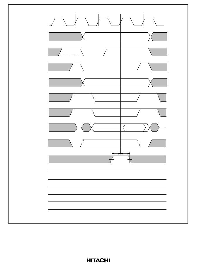
420
T
1
T
w
T
2
CKIO
BS
CSn
RD/
WR
,
WE
RD
WEn
,
CASxx
,
DQMxx
RAS
,
CE
CAS
,
OE
CKE
D31D0
DACKn
WAIT
A26A0
t
WTH
t
WTS
Notes: 1.
2.
The dotted line shows the waveform when synchronous DRAM is connected.
The DACKn waveform shown is for the case where active-high has been specified.
Figure 15.18 Basic Bus Cycle (1 Wait Cycle)
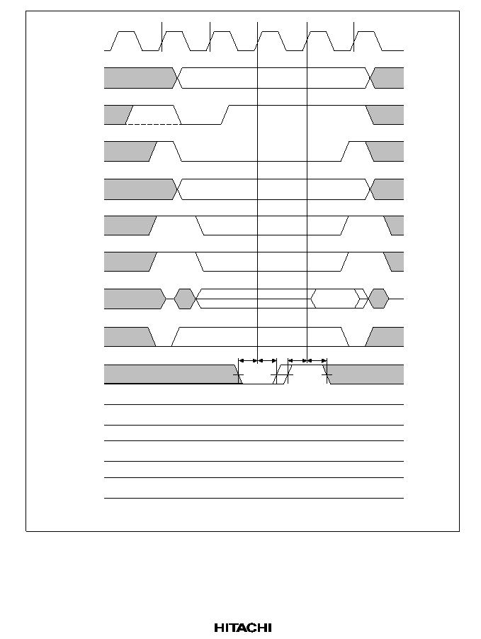
421
T
1
T
w
T
wx
T
2
CKIO
BS
CSn
RD/
WR
,
WE
RD
WEn
,
CASxx
,
DQMxx
RAS
,
CE
CAS
,
OE
CKE
D31D0
DACKn
WAIT
A26A0
t
WTS
t
WTH
t
WTS
t
WTH
Notes: 1.
2.
The dotted line shows the waveform when synchronous DRAM is connected.
The DACKn waveform shown is for the case where active-high has been specified.
Figure 15.19 Basic Bus Cycle (External Wait Input)

422
CKIO
BS
CSn
RD/
WR
,
WE
RD
WEn
,
CASxx
,
DQMxx
RAS
,
CE
CAS
,
OE
CKE
D31D0
DACKn
WAIT
Upper
address
Lower
address
T
r
T
c
T
d1
T
d2
T
d3
T
d4
t
AD
t
AD
t
AD
t
AD
t
AD
t
AD
t
BSD
t
BSD
t
BSD
t
RWD
t
CSD1
t
CSD1
t
RWD
t
DQMD
t
RDS3
t
DACD2
t
DACD2
t
DACD2
t
DACD2
t
RDH4
t
RDS3
t
RDH4
t
RDS3
t
RDH4
t
RDS3
t
RDH4
t
DACD1
t
DACD1
t
RASD1
t
RASD1
t
RASD1
t
CASD1
t
CASD1
t
CASD1
t
CASD1
t
DACD1
t
DACD1
t
DQMD
t
RSD1
Notes: 1.
2.
The dotted line shows the waveform when synchronous DRAM in another CS space
is accessed.
The DACKn waveform shown is for the case where active-high has been specified.
Figure 15.20 Synchronous DRAM Read Bus Cycle
(RCD = 1 Cycle, CAS Latency = 1 Cycle, Bursts = 4, PLL On)

423
CKIO
BS
CSn
RD/
WR
,
WE
RD
WEn
,
CASxx
,
DQMxx
RAS
,
CE
CAS
,
OE
CKE
D31D0
WAIT
Upper
address
Lower
address
T
r
T
c
T
d1
T
d2
T
d3
T
d4
t
AD
t
AD
t
AD
t
BSD
t
BSD
t
BSD
t
BSD
t
RWD
t
CSD1
t
CSD1
t
RWD
t
DQMD
t
RDS3
t
RDH4
t
RASD1
t
RASD1
t
RASD1
t
CASD1
t
CASD1
t
CASD1
t
CASD1
t
DQMD
t
RSD1
Note:
The dotted line shows the waveform when synchronous DRAM in another CS space is
accessed.
Figure 15.21 Synchronous DRAM Single Read Bus Cycle
(RCD = 1 Cycle, CAS Latency = 1 Cycle, Bursts = 4, PLL On)
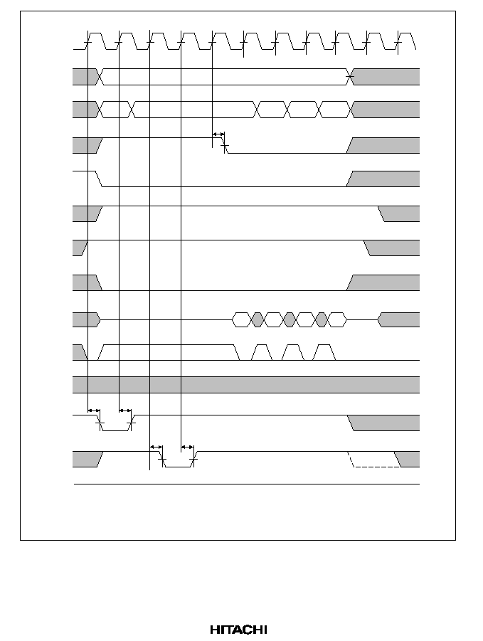
424
CKIO
BS
CSn
RD/
WR
,
WE
RD
WEn
,
CASxx
,
DQMxx
RAS
,
CE
CAS
,
OE
CKE
D31D0
DACKn
WAIT
Upper
address
Lower
address
T
r
T
rw
T
c
T
w
T
d1
T
d2
T
d3
T
d4
t
BSD
t
RASD1
t
CASD1
t
CASD1
t
RASD1
Notes: 1.
2.
The dotted line shows the waveform when synchronous DRAM in another CS space
is accessed.
The DACKn waveform shown is for the case where active-high has been specified.
Figure 15.22 Synchronous DRAM Read Bus Cycle
(RCD = 2 Cycles, CAS Latency = 2 Cycles, Bursts = 4)

425
CKIO
BS
CSn
RD/
WR
,
WE
RD
WEn
,
CASxx
,
DQMxx
CAS
,
OE
CKE
D31D0
DACKn
WAIT
RAS
,
CE
Upper
address
Lower
address
T
nop
T
c
T
d1
T
d2
T
d3
T
d4
t
AD
t
BSD
t
RWD
t
CSD1
t
DQMD
t
DACD1
t
RASD1
t
CASD1
t
CASD1
t
CASD1
t
CASD1
Note:
The DACKn waveform shown is for the case where active-high has been specified.
Figure 15.23 Synchronous DRAM Read Bus Cycle
(Bank Active, Same Row Access, CAS Latency = 1 Cycle)
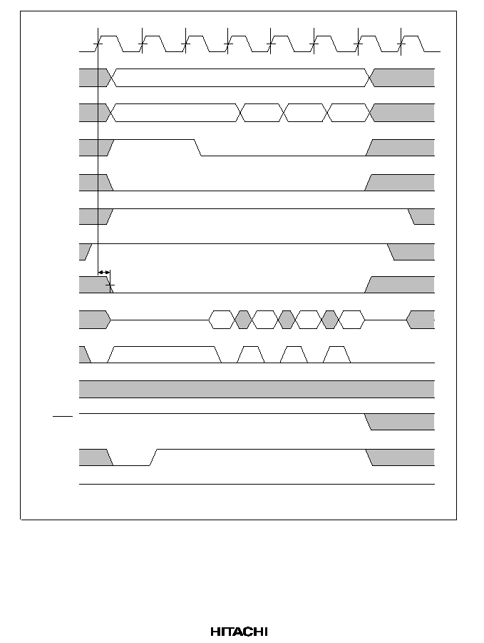
426
Upper
address
Lower
address
BS
CKIO
T
C
T
W
T
d1
T
d2
T
d3
T
d4
CSn
RD/
WR
WE
RD
WEn
CASxx
DQMxx
D31D0
DACKn
WAIT
RAS
CE
CAS
OE
CKE
t
DQMD
Note:
The DACKn waveform shown is for the case where active-high has been specified.
Figure 15.24 Synchronous DRAM Read Bus Cycle
(Bank Active, Same Row Access, CAS Latency = 2 Cycles)
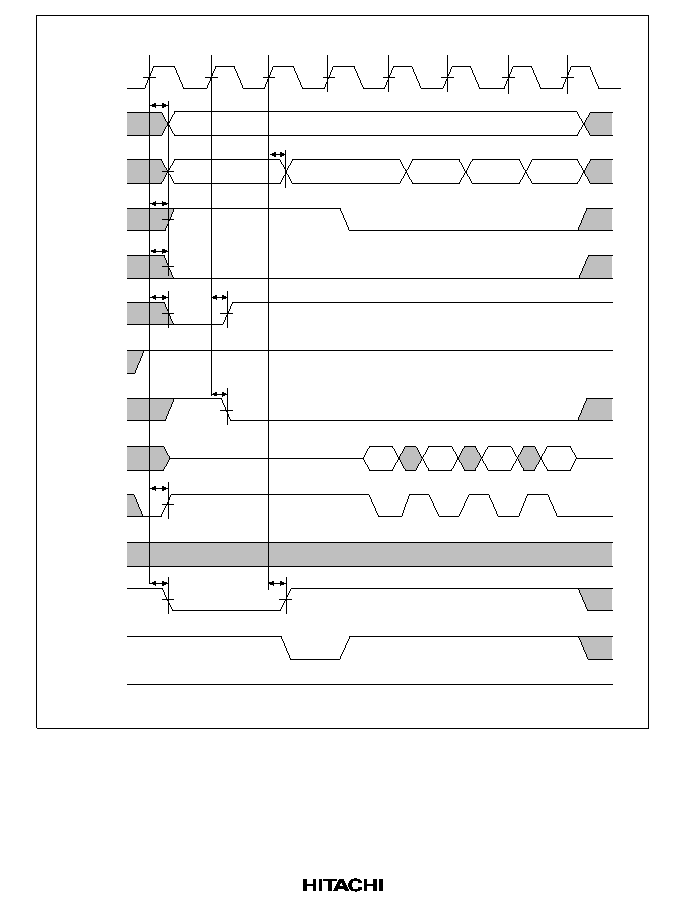
427
Upper
address
Lower
address
BS
CKIO
T
p
T
r
T
c
T
d1
T
d2
T
d3
T
d4
CSn
RD/
WR
WE
RD
WEn
CASxx
DQMxx
D31D0
DACKn
WAIT
RAS
CE
CAS
OE
CKE
t
AD
t
AD
t
BSD
t
CSD1
t
RWD
t
RWD
t
DACD1
t
RASD1
t
RASD1
t
DQMD
Note:
The DACKn waveform shown is for the case where active-high has been specified.
Figure 15.25 Synchronous DRAM Read Bus Cycle (Bank Active, Different Row Access,
TRP = 1 Cycle, RCD = 1 Cycle, CAS Latency = 1 Cycle)

428
Upper
address
Lower
address
BS
CKIO
T
p
T
pw
T
r
T
c
T
d1
T
d4
CSn
RD/
WR
WE
RD
WEn
CASxx
DQMxx
D31D0
DACKn
WAIT
RAS
CE
CAS
OE
CKE
t
RWD
t
RASD1
t
RASD1
Note:
The DACKn waveform shown is for the case where active-high has been specified.
Figure 15.26 Synchronous DRAM Read Bus Cycle (Bank Active, Different Row Access,
TRP = 2 Cycles, RCD = 1 Cycle, CAS Latency = 1 Cycle)

429
CKIO
T
r
T
c
T
ap
Upper
address
WEn
CASxx
DQMxx
D31D0
Lower
address
BS
CSn
RD
RD/
WR
WE
DACKn
WAIT
RAS
CE
CAS
OE
CKE
t
AD
t
AD
t
AD
t
BSD
t
CSD1
t
RWD
t
DQMD
t
DACD1
t
RASD1
t
RASD1
t
CASD1
t
CASD1
t
CASD1
t
RASD1
t
RASD1
t
DQMD
t
DACD1
t
DACD2
t
DON
t
WDD
t
RWD
t
RWD
t
RSD1
t
CSD1
t
CSD1
t
BSD
t
BSD
t
WDH1
Notes: 1.
2.
Dotted lines show the waveforms when synchronous DRAM in another CS space
is accessed.
The DACKn waveform shown is for the case where active-high has been specified.
t
DOF
Figure 15.27 Synchronous DRAM Write Bus Cycle
(RCD = 1 Cycle, TRWL = 1 Cycle, PLL On)
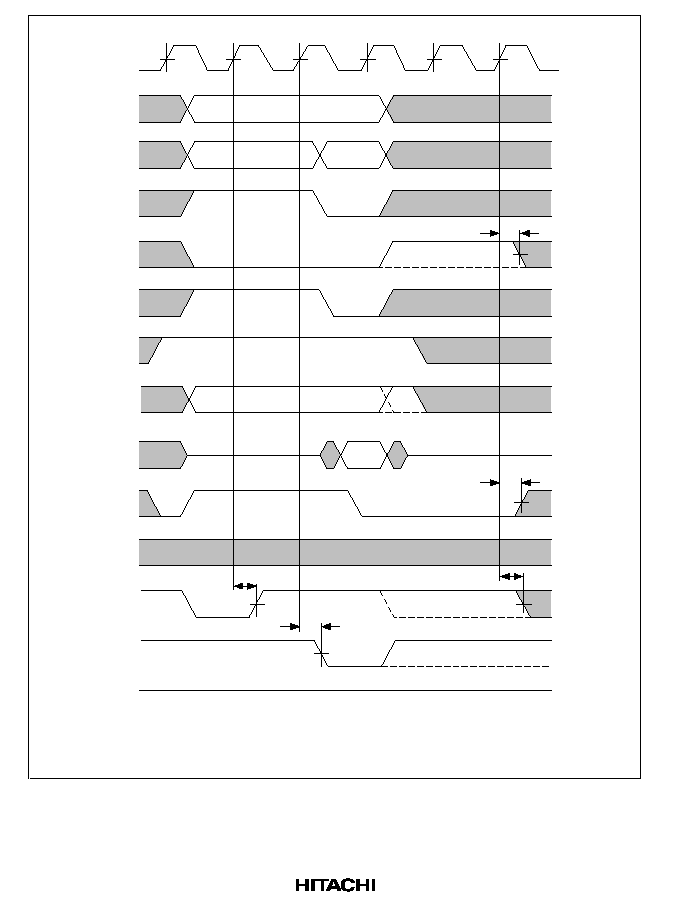
430
Tr
Trw
Tc
Trwl
Tap
CKIO
Upper
address
Lower
address
BS
CSn
RD/
WR
WE
RD
WEn
CASxx
DQMxx
D31D0
DACKn
WAIT
RAS
CE
CAS
OE
CKE
t
RASD1
t
CASD1
t
RASD1
t
DACD1
t
CSD1
Notes: 1.
2.
Dotted lines show the waveforms when synchronous DRAM in another CS space
is accessed.
The DACKn waveform shown is for the case where active-high has been specified.
Figure 15.28 Synchronous DRAM Write Bus Cycle
(RCD = 2 Cycles, TRWL = 2 Cycles)
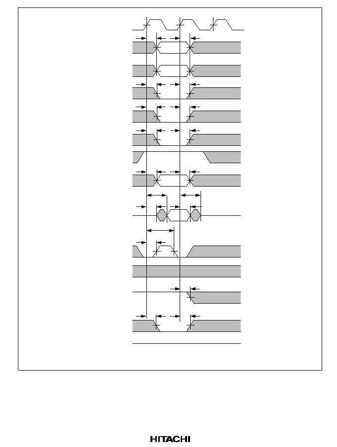
431
Tc
CKIO
Upper
address
Lower
address
BS
CSn
RD/
WR
WE
RD
WEn
CASxx
DQMxx
D31D0
DACKn
WAIT
RAS
CE
CAS
OE
CKE
t
AD
t
AD
t
BSD
t
BSD
t
CSD1
t
CSD1
t
RWD
t
RWD
t
DQMD
t
DQMD
t
WDD
t
DOF
t
WDH1
t
DON
t
DACD2
t
DACD1
t
RASD1
t
CASD1
t
CASD1
Note:
The DACKn waveform shown is for the case where active-high has been specified.
Figure 15.29 Synchronous DRAM Write Bus Cycle (Bank Active, Same Row Access)
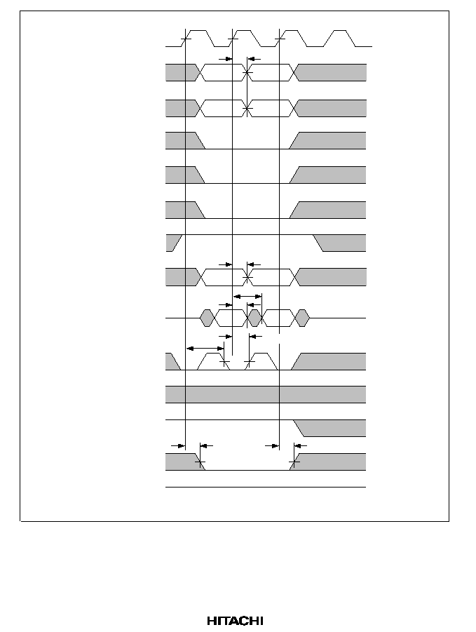
432
Tc
CKIO
Upper
address
Lower
address
BS
CSn
RD/
WR
WE
RD
WEn
CASxx
DQMxx
D31D0
DACKn
WAIT
RAS
CE
CAS
OE
CKE
t
AD
Tc
t
DQMD
t
WDD
t
WDH1
t
DACD2
t
DACD1
t
CASD1
t
CASD1
Note:
The DACKn waveform shown is for the case where active-high has been specified.
Figure 15.30 Synchronous DRAM Consecutive Write Cycles
(Bank Active, Same Row Access)
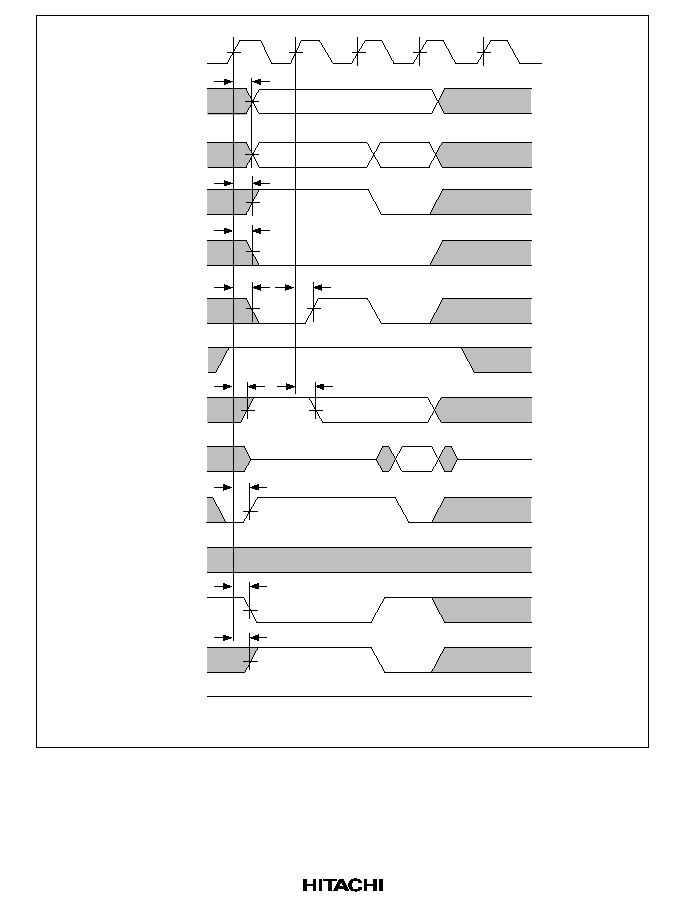
433
CKIO
Upper
address
Lower
address
BS
CSn
RD/
WR
WE
RD
WEn
CASxx
DQMxx
D31D0
DACKn
WAIT
RAS
CE
CAS
OE
CKE
t
AD
Tp
Tr
Tc
t
BSD
t
CSD1
t
RWD
t
RWD
t
DQMD
t
DQMD
t
DACD1
t
RASD1
t
CASD1
Note:
The DACKn waveform shown is for the case where active-high has been specified.
Figure 15.31 Synchronous DRAM Write Bus Cycle
(Bank Active, Different Row Access, TRP = 1 Cycle, RCD = 1 Cycle)

434
Upper
address
Lower
address
BS
CKIO
Tp
T
pw
T
r
T
rw
T
c
CSn
RD/
WR
WE
RD
WEn
CASxx
DQMxx
D31D0
DACKn
WAIT
RAS
CE
CAS
OE
CKE
t
RWD
t
DQMD
t
RASD1
t
RASD1
Note:
The DACKn waveform shown is for the case where active-high has been specified.
Figure 15.32 Synchronous DRAM Write Bus Cycle
(Bank Active, Different Row Access, TRP = 2 Cycles, RCD = 2 Cycles)

435
CKIO
BS
RD
CSn
RD/
WR
,
WE
WEn
,
CASxx
,
DQMxx
RAS
,
CE
CAS
,
OE
CKE
D31D0
DACKn
WAIT
Upper
address
T
p
T
mw
t
AD
t
BSD
t
AD
Lower
address
t
AD
t
CSD1
t
RWD
t
RWD
t
DQMD
t
CSD1
t
CSD1
t
RASD1
t
RASD1
t
RASD1
t
CSD1
t
CSD1
t
BSD
Figure 15.33 Synchronous DRAM Mode Register Write Cycle (TRP = 1 Cycle)

436
CKIO
BS
RD
CSn
RD/
WR
,
WE
WEn
,
CASxx
,
DQMxx
RAS
,
CE
CAS
,
OE
CKE
D31D0
DACKn
WAIT
Upper
address
T
p
T
pw
T
mw
Lower
address
t
RWD
t
RWD
t
RASD1
t
RASD1
Figure 15.34 Synchronous DRAM Mode Register Write Cycle (TRP = 2 Cycles)

437
CKIO
BS
CSn
RD
RD/
WR
,
WE
WEn
,
CASxx
,
DQMxx
RAS
,
CE
CAS
,
OE
CKE
D31D0
DACKn
WAIT
Upper
address
T
rr
T
rc1
T
re
T
nop
T
rc2
Lower
address
t
RASD1
t
RASD1
t
RASD1
t
CASD1
t
CASD1
t
AD
t
AD
t
CSD1
t
RWD
t
RWD
t
BSD
t
CSD1
Note:
A precharge cycle always precedes the auto-refresh cycle by the number of cycles
specified by TRP.
Figure 15.35 Synchronous DRAM Auto-Refresh Cycle (TRAS = 2 Cycles)

438
CKIO
BS
RD
CSn
RD/
WR
,
WE
WEn
,
CASxx
,
DQMxx
RAS
,
CE
CAS
,
OE
D31D0
DACKn
WAIT
Upper
address
T
p
T
rr
T
rc2
T
re
T
nop
T
rc1
Lower
address
CKE
t
RASD1
t
CASD1
t
AD
t
AD
t
BSD
t
CSD1
t
RWD
t
RWD
Figure 15.36 Synchronous DRAM Auto-Refresh Cycle
(Shown From Precharge Cycle, TRP = 1 Cycle, TRAS = 2 Cycles)
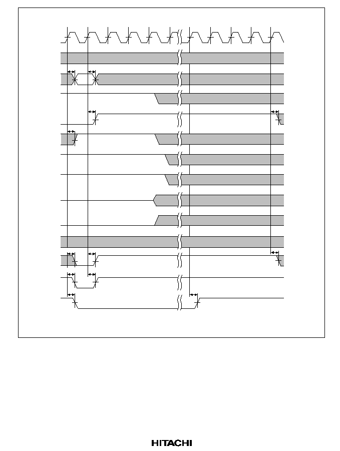
439
Upper
address
Lower
address
BS
CKIO
Trr
T
rc1
T
rc2
T
re
T
rc1
CSn
RD/
WR
WE
WEn
CASxx
DQMxx
D31D0
DACKn
RD
WAIT
RAS
CE
CAS
OE
CKE
Note: A precharge cycle always precedes the self-refresh cycle by the number of cycles specified
by TRP.
t
AD
t
RWD
t
AD
t
RASD1
t
CASD1
t
CKED
t
CKED
t
RASD1
t
CSD1
t
CSD1
T
re
T
nap
t
RASD1
t
CASD1
Figure 15.37 Synchronous DRAM Self-Refresh Cycle (TRAS = 2)

440
Upper
address
Lower
address
BS
CKIO
Tr
T
c
T
d1
T
d2
T
d3
T
d4
CSn
RD/
WR
WE
RD
WEn
CASxx
DQMxx
D31D0
DACKn
WAIT
RAS
CE
CAS
OE
CKE
t
AD
t
AD
t
AD
t
AD
t
AD
t
AD
t
BSD
t
RASD1
t
RASD1
t
RASD1
t
CASD1
t
CSD1
t
RWD
t
DQMD
t
RDS2
t
DACD1
t
DQMD
t
RWD
t
BSD
t
CASD1
t
CASD1
t
CASD1
t
RSD2
t
RDS2
t
RDH3
t
RDH3
t
RDH3
t
RDH3
t
RDS2
t
RDS2
t
DACD3
t
DACD3
t
DACD1
t
DACD1
t
DACD3
t
DACD3
t
DACD1
t
CSD1
t
BSD
Notes: 1.
2.
The dotted line shows the waveform when synchronous DRAM in another CS space
is accessed.
The DACKn waveform shown is for the case where active-high has been specified.
Figure 15.38 Synchronous DRAM Read Bus Cycle
(RCD = 1 Cycle, CAS Latency = 1 Cycle, TRP = 1 Cycle, Bursts = 4, PLL Off)
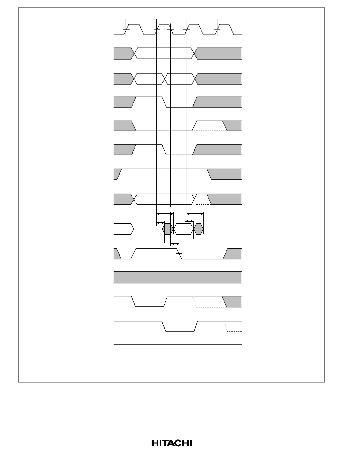
441
CKIO
T
r
T
c
T
ap
Upper
address
Lower
address
WEn
CASxx
DQMxx
BS
CSn
RD/
WR
WE
RD
D31D0
DACKn
WAIT
RAS
CE
CAS
OE
CKE
t
WDD
t
DON
t
DACD3
t
WDH1
t
DOF
Notes: 1.
2.
Dotted lines show the waveforms when synchronous DRAM in another CS space
is accessed.
The DACKn waveform shown is for the case where active-high has been specified.
Figure 15.39 Synchronous DRAM Write Bus Cycle
(RCD = 1 Cycle, TRWL = 1 Cycle, PLL Off)

442
CKIO
T
p
T
r
T
c1
T
c2
t
AD
t
AD
t
BSD
t
BSD
t
RDS1
t
DACD2
t
AD
BS
CSn
RD/
WR
,
WE
RD
WEn
,
CASxx
,
DQMxx
RAS
,
CE
CAS
,
OE
CKE
D31D0
DACKn
WAIT
Upper
address
Lower
address
t
BSD
t
RSD1
t
RSD1
t
CASD2
t
CASD2
t
CSD1
t
CSD1
t
RWD
t
RWD
t
CASD2
t
RASD2
t
RASD2
t
RASD2
t
RDH5
t
DACD1
t
RSD1
Notes: 1.
2.
t
RDH5
is specified from the rise of
RD
or
CASxx
, whichever is first.
The DACKn waveform shown is for the case where active-high has been specified.
Figure 15.40 DRAM Read Cycle (TRP = 1 Cycle, RCD = 1 Cycle, No Waits, PLL On)

443
CKIO
T
p
T
r
T
c1
T
c2
t
AD
t
AD
t
BSD
t
BSD
t
DACD2
t
AD
BS
CSn
RD/
WR
,
WE
RD
WEn
,
CASxx
,
DQMxx
RAS
,
CE
CAS
,
OE
CKE
D31D0
DACKn
WAIT
Upper
address
Lower
address
t
BSD
t
CASD2
t
CASD2
t
CSD1
t
CSD1
t
RWD
t
RWD
t
CASD2
t
RASD2
t
RASD2
t
RASD2
t
DACD1
t
RSD1
t
RWD
t
DON
t
WDH1
t
WDD
t
DOF
Note:
The DACKn waveform shown is for the case where active-high has been specified.
Figure 15.41 DRAM Write Cycle
(TRP = 1 Cycle, RCD = 1 Cycle, No Waits, PLL On)

444
CKIO
BS
CSn
RD/
WR
,
WE
RD
WEn
,
CASxx
,
DQMxx
RAS
,
CE
CAS
,
OE
CKE
D31D0
DACKn
WAIT
Upper
address
Lower
address
T
p
T
pw
T
r
T
rw
T
c1
T
c2
T
w
t
WTH
t
WTS
Note:
The DACKn waveform shown is for the case where active-high has been specified.
Figure 15.42 DRAM Bus Cycle (TRP = 2 Cycles, RCD = 2 Cycles, 1 Wait)

445
CKIO
T
p
T
r
T
c1
T
w
T
wx
T
c2
BS
CSn
RD/
WR
,
WE
RD
WEn
,
CASxx
,
DQMxx
RAS
,
CE
CAS
,
OE
CKE
D31D0
DACKn
WAIT
Upper
address
Lower
address
t
WTS
t
WTH
t
WTS
t
WTH
Note:
The DACKn waveform shown is for the case where active-high has been specified.
Figure 15.43 DRAM Bus Cycle (TRP = 1 Cycle, RCD = 1 Cycle, External Wait Input)
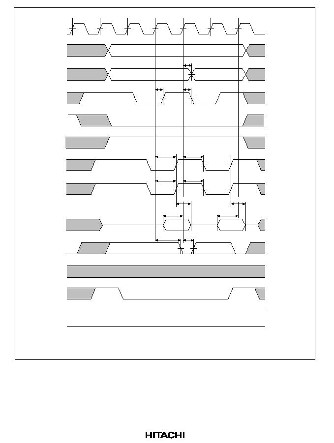
446
CKIO
T
p
T
r
T
c1
T
c2
T
c1
T
c2
t
AD
t
BSD
t
DACD1
BS
RD/
WR
,
WE
RD
WEn
,
CASxx
,
DQMxx
RAS
,
CE
CAS
,
OE
CKE
D31D0
DACKn
WAIT
Upper
address
Lower
address
t
RSD1
t
RSD1
t
CASD2
t
CASD2
t
DACD2
t
RDS1
CSn
t
BSD
t
RDH5
t
RDS1
t
RDH5
Notes: 1.
2.
t
RDH5
is specified from the rise of
RD
or
CASxx
, whichever is first.
The DACKn waveform shown is for the case where active-high has been specified.
Figure 15.44 DRAM Burst Read Cycle
(TRP = 1 Cycle, RCD = 1 Cycle, No Waits, PLL On)
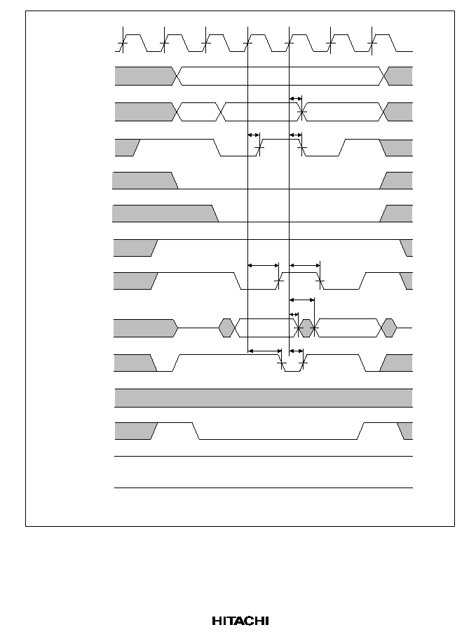
447
CKIO
T
p
T
r
T
c1
T
c2
T
c1
T
c2
t
AD
t
BSD
t
DACD1
BS
CSn
RD/
WR
,
WE
RD
WEn
,
CASxx
,
DQMxx
RAS
,
CE
CAS
OE
CKE
D31D0
DACKn
WAIT
Upper
address
Lower
address
t
WDH1
t
BSD
t
CASD2
t
CASD2
t
WDD
t
DACD2
Note:
The DACKn waveform shown is for the case where active-high has been specified.
Figure 15.45 DRAM Burst Write Cycle
(TRP = 1 Cycle, RCD = 1 Cycle, No Waits, PLL On)

448
CKIO
BS
CSn
RD/
WR
,
WE
RD
WEn
,
CASxx
,
DQMxx
RAS
,
CE
CAS
,
OE
CKE
D31D0
DACKn
WAIT
Upper
address
Lower
address
T
p
t
CSD1
T
rr
T
rc1
T
rc2
T
re
t
CASD2
t
CASD2
t
CASD2
t
RASD2
t
RASD2
t
RASD2
t
CSD1
Figure 15.46 DRAM CAS-Before-RAS Refresh Cycle
(TRP = 1 Cycle, TRAS = 2 Cycles, PLL On)

449
CKIO
T
p
T
r
T
c1
T
c2
t
AD
t
AD
t
BSD
t
BSD
t
RDS2
t
DACD3
t
AD
BS
CSn
RD/
WR
,
WE
RD
WEn
,
CASxx
,
DQMxx
RAS
,
CE
CAS
,
OE
CKE
D31D0
DACKn
WAIT
Upper
address
Lower
address
t
BSD
t
RSD2
t
RSD2
t
CASD3
t
CASD3
t
CSD1
t
CSD1
t
RWD
t
RWD
t
CASD3
t
RASD3
t
ASR
t
RASD3
t
ASC
t
RDH5
t
DACD1
t
RASD3
t
RSD2
Notes: 1.
2.
t
RDH5
is specified from the rise of
RD
or
CASxx
, whichever is first.
The DACKn waveform shown is for the case where active-high has been specified.
Figure 15.47 DRAM Read Cycle (TRP = 1 Cycle, RCD = 1 Cycle, No Waits, PLL Off)

450
CKIO
T
p
T
r
T
c1
T
c2
t
AD
t
AD
t
BSD
t
BSD
t
DON
t
WDH1
t
DACD3
t
AD
BS
CSn
RD/
WR
,
WE
RD
WEn
,
CASxx
,
DQMxx
RAS
,
CE
CAS
,
OE
CKE
D31D0
DACKn
WAIT
Upper
address
Lower
address
t
BSD
t
RSD2
t
CASD3
t
WCS
t
ASC
t
CSD1
t
CSD1
t
RWD
t
RWD
t
CASD3
t
RASD3
t
ASR
t
WDD
t
DOF
t
DACD1
t
RASD3
t
RWD
t
CASD3
t
WDS
Note:
The DACKn waveform shown is for the case where active-high has been specified.
Figure 15.48 DRAM Write Cycle (TRP = 1 Cycle, RCD = 1 Cycle, No Waits, PLL Off)
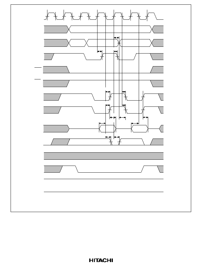
451
CKIO
T
p
T
r
T
c1
T
c2
T
c1
T
c2
t
AD
t
BSD
t
DACD1
BS
CSn
RD/
WR
,
WE
RD
WEn
,
CASxx
,
DQMxx
RAS
,
CE
CAS
,
OE
CKE
D31D0
DACKn
WAIT
Upper
address
Lower
address
t
RDH5
t
RDS2
t
BSD
t
RSD2
t
CASD3
t
CASD3
t
RDH5
t
RDS2
t
DACD3
t
RSD2
t
ASC
Notes: 1.
2.
t
RDH5
is specified from the rise of
RD
or
CASxx
, whichever is first.
The DACKn waveform shown is for the case where active-high has been specified.
Figure 15.49 DRAM Burst Read Cycle
(TRP = 1 Cycle, RCD = 1 Cycle, No Waits, PLL Off)
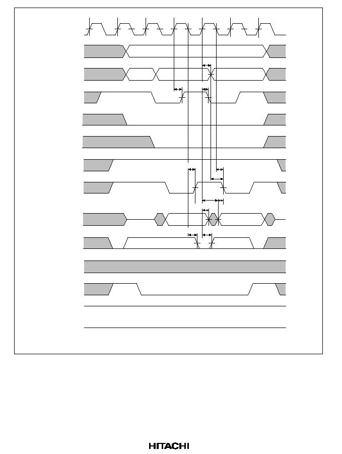
452
CKIO
T
p
T
r
T
c1
T
c2
T
c1
T
c2
t
AD
t
BSD
t
DACD1
BS
CSn
RD/
WR
,
WE
RD
WEn
,
CASxx
,
DQMxx
RAS
,
CE
CAS
,
OE
CKE
D31D0
DACKn
WAIT
Upper
address
Lower
address
t
BSD
t
CASD3
t
ASC
t
CASD3
t
WDD
t
DACD3
t
WDS
t
WDH1
Note:
The DACKn waveform shown is for the case where active-high has been specified.
Figure 15.50 DRAM Burst Write Cycle
(TRP = 1 Cycle, RCD = 1 Cycle, No Waits, PLL Off)
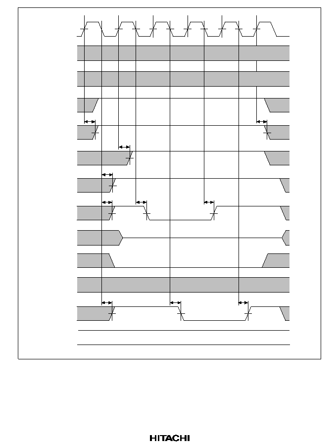
453
CKIO
BS
CSn
RD/
WR
,
WE
RD
WEn
,
CASxx
,
DQMxx
RAS
,
CE
CAS
,
OE
CKE
D31D0
DACKn
WAIT
Upper
address
Lower
address
T
p
t
CSD1
T
rr
T
rc1
T
rc2
T
re
t
RWD
t
RSD2
t
CASD3
t
CASD3
t
RASD3
t
RASD3
t
CSD1
t
CASD3
t
RASD3
Figure 15.51 DRAM CAS-Before-RAS Refresh Cycle
(TRP = 1 Cycle, TRAS = 2 Cycles, PLL Off)
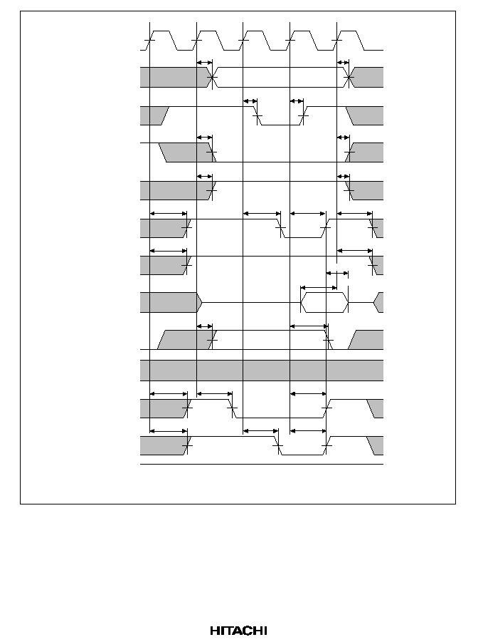
454
CKIO
T
p
T
r
T
c1
T
c2
t
AD
t
BSD
t
RDS1
t
DACD2
t
AD
BS
CSn
RD/
WR
,
WE
RD
WEn
,
CASxx
,
DQMxx
RAS
,
CE
CAS
,
OE
CKE
D31D0
DACKn
WAIT
Upper
address
t
BSD
t
RSD1
t
RSD1
t
RSD1
t
WED1
t
CSD1
t
CSD1
t
RWD
t
RWD
t
WED1
t
CED1
t
CED1
t
CED1
t
DACD1
t
RSD1
t
OED1
t
OED1
t
OED1
t
RDH6
Note:
The DACKn waveform shown is for the case where active-high has been specified.
Figure 15.52 Pseudo-SRAM Read Cycle
(PLL On, TRP = 1 Cycle, RCD = 1 Cycle, No Waits)

455
CKIO
T
p
T
r
T
c1
T
c2
t
AD
t
BSD
t
DACD2
t
AD
BS
CSn
RD/
WR
,
WE
RD
WEn
,
CASxx
,
DQMxx
RAS
,
CE
CAS
,
OE
CKE
D31D0
DACKn
WAIT
Address
t
BSD
t
WED1
t
WED1
t
WED1
t
RSD1
t
CSD1
t
CSD1
t
RSD1
t
CED1
t
CED1
t
CED1
t
DACD1
t
WED1
t
OED1
t
DOF
t
WDD
t
RWD
t
RWD
t
DON
t
WDH1
Note:
The DACKn waveform shown is for the case where active-high has been specified.
Figure 15.53 Pseudo-SRAM Write Cycle
(PLL On, TRP = 1 Cycle, RCD = 1 Cycle, No Waits)

456
CKIO
BS
CSn
RD/
WR
,
WE
RD
WEn
,
CASxx
,
DQMxx
RAS
,
CE
CAS
,
OE
CKE
D31D0
DACKn
WAIT
Address
T
p
T
pw
T
r
T
rw
T
c1
T
c2
T
w
t
WTH
t
WTS
Note:
The DACKn waveform shown is for the case where active-high has been specified.
Figure 15.54 Pseudo-SRAM Bus Cycle (TRP = 2 Cycles, RCD = 2 Cycles, 1 Wait)

457
CKIO
T
p
T
r
T
c1
T
w
T
wx
T
c2
BS
CSn
RD/
WR
,
WE
RD
WEn
,
CASxx
,
DQMxx
RAS
,
CE
CAS
,
OE
CKE
D31D0
DACKn
WAIT
Address
t
WTS
t
WTH
t
WTS
t
WTH
Note:
The DACKn waveform shown is for the case where active-high has been specified.
Figure 15.55 Pseudo-SRAM Bus Cycle
(TRP = 1 Cycle, RCD = 1 Cycle, External Wait Input)

458
CKIO
T
p
T
r
T
c1
T
c2
T
c1
T
c2
t
AD
t
BSD
t
DACD1
BS
RD/
WR
,
WE
RD
WEn
,
CASxx
,
DQMxx
RAS
,
CE
CAS
,
OE
CKE
D31D0
DACKn
WAIT
Upper
address
Lower
address
t
RSD1
t
RSD1
t
OED1
t
OED1
t
DACD2
t
RDS1
CSn
t
BSD
t
RDH6
t
RDS1
t
RDH6
Note:
The DACKn waveform shown is for the case where active-high has been specified.
Figure 15.56 Pseudo-SRAM Read Cycle
(Static Column Mode, PLL On, TRP = 1 Cycle, RCD = 1 Cycle, No Waits)
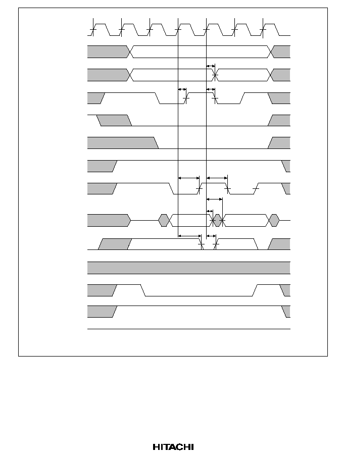
459
CKIO
T
p
T
r
T
c1
T
c2
T
c1
T
c2
t
AD
t
BSD
t
DACD1
BS
CSn
RD/
WR
,
WE
RD
WEn
,
CASxx
,
DQMxx
RAS
,
CE
CAS
,
OE
CKE
D31D0
DACKn
WAIT
Upper
address
Lower
address
t
BSD
t
WED1
t
WED1
t
WDD
t
DACD2
t
WDH1
Note:
The DACKn waveform shown is for the case where active-high has been specified.
Figure 15.57 Pseudo-SRAM Write Cycle
(Static Column Mode, PLL On, TRP = 1 Cycle, RCD = 1 Cycle, No Waits)
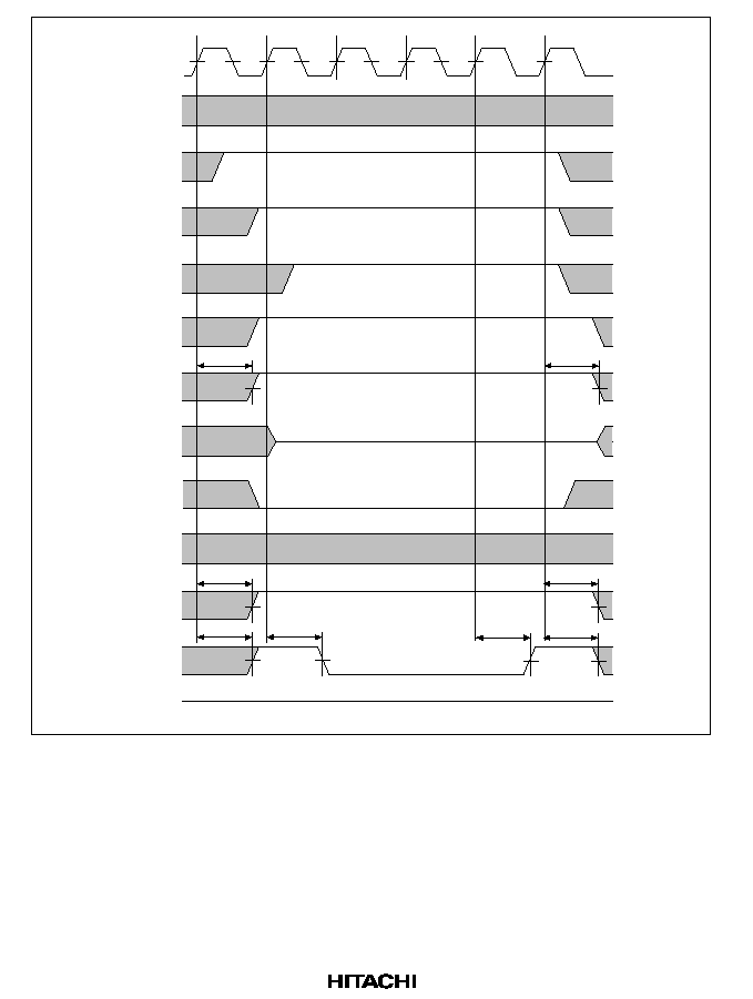
460
CKIO
BS
Address
T
p
T
rr
T
rc1
T
rc2
T
re
WAIT
CSn
RD/
WR
,
WE
RD
D31D0
DACKn
WEn
,
CASxx
,
DQMxx
RAS
,
OE
CAS
,
OE
CKE
t
WED1
t
CED1
t
CED1
t
OED1
t
OED1
t
OED1
t
OED1
t
WED1
Figure 15.58 Pseudo-SRAM Auto-Refresh Cycle
(PLL On, TRP = 1 Cycle, TRAS = 2 Cycles)

461
CKIO
Address
WAIT
BS
CSn
RD/
WR
,
WE
RD
WEn
,
CASxx
,
DQMxx
DACKn
RAS
,
CE
CKE
D31D0
CAS
,
OE
T
p
T
rc
T
rc1
T
rc2
T
rc1
T
re
t
WED1
t
CED1
t
OED1
t
OED1
t
OED1
t
OED1
t
CED1
Figure 15.59 Pseudo-SRAM Self-Refresh Cycle
(PLL On, TRP = 1 Cycle, TRAS = 2 Cycles)
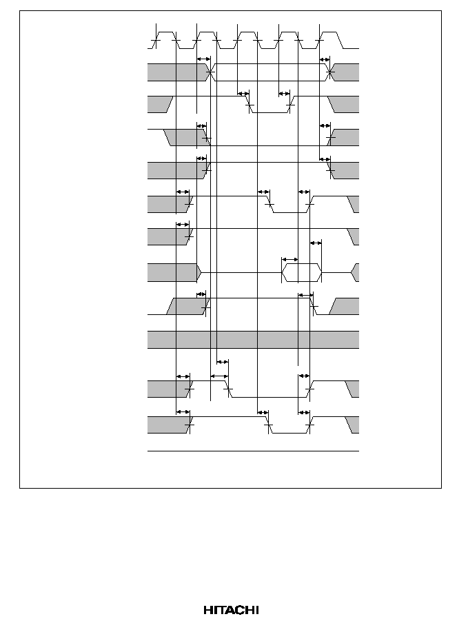
462
CKIO
Address
T
p
T
r
T
c1
T
c2
BS
CSn
RD/
WR
,
WE
RD
WEn
,
CASxx
,
DQMxx
RAS
,
CE
CKE
D31D0
DACKn
WAIT
CAS
,
OE
t
AD
t
RSD2
t
BSD
t
BSD
t
CSD1
t
RWD
t
AD
t
RSD2
t
RSD2
t
RDH6
t
RDS2
t
OED2
t
CED2
t
AS2
t
CED2
t
CSD1
t
RWD
t
DACD1
t
DACD3
t
OED2
t
CED2
t
OED2
t
WED2
Note:
The DACKn waveform shown is for the case where active-high has been specified.
Figure 15.60 Pseudo-SRAM Read Cycle
(PLL Off, TRP = 1 Cycle, RCD = 1 Cycle, No Waits)

463
CKIO
Address
T
p
T
r
T
c1
T
c2
BS
CSn
RD/
WR
,
WE
RD
WEn
,
CASxx
,
DQMxx
RAS
,
CE
CKE
D31D0
DACKn
WAIT
CAS
,
OE
t
AD
t
RWD
t
BSD
t
BSD
t
CSD1
t
RWD
t
AD
t
WED2
t
WDD
t
DON
t
DOF
t
WDH1
t
CED2
t
CED2
t
AS2
t
CED2
t
OED2
t
CSD1
t
RWD
t
RSD2
t
WED2
t
WED2
t
DACD1
t
DACD3
t
WDH3
Note:
The DACKn waveform shown is for the case where active-high has been specified.
Figure 15.61 Pseudo-SRAM Write Cycle
(PLL Off, TRP = 1 Cycle, RCD = 1 Cycle, No Waits)

464
Upper
address
Lower
address
CKIO
BS
CSn
D31D0
CSn
WAIT
WEn
,
CASxx
DQMxx
RD/
WR
,
WE
RD
CAS
,
OE
CKE
RAS
,
CE
T
p
T
r
T
c1
T
c2
T
c1
T
c2
t
AD
t
BSD
t
BSD
t
RSD2
t
RSD2
t
RDH6
t
RDS2
t
OED2
t
DACD1
t
RDS2
t
RDH6
t
DACD3
t
OED2
Note:
The DACKn waveform shown is for the case where active-high has been specified.
Figure 15.62 Pseudo-SRAM Read Cycle
(Static Column Mode, PLL Off, TRP = 1 Cycle, RCD = 1 Cycle, No Waits)
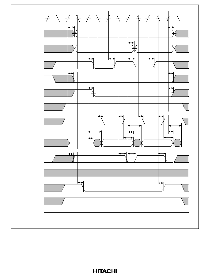
465
Upper
address
Lower
address
CKIO
BS
CSn
D31D0
DACKn
WAIT
WEn
,
CASxx
,
DQMxx
RD/
WR
,
WE
RD
CAS
,
OE
CKE
RAS
,
CE
T
p
T
r
T
c1
T
c2
T
c1
T
c2
t
AD
t
BSD
t
BSD
t
CSD1
t
RWD
t
WED2
t
DOF
t
WDH1
t
BSD
t
BSD
t
AD
t
WDD
t
WDH1
t
RWD
t
WED2
t
DACD1
t
AD
t
DACD3
t
CED2
t
DON
t
CED2
t
WDD
t
WED2
t
WDH3
t
WDH3
t
DACD1
t
DACD3
t
WED2
t
CSD1
Note:
The DACKn waveform shown is for the case where active-high has been specified.
Figure 15.63 Pseudo-SRAM Write Cycle
(Static Column Mode, PLL Off, TRP = 1 Cycle, RCD = 1 Cycle, No Waits)

466
CKIO
BS
Address
T
p
T
rr
T
rc1
T
rc2
T
re
WAIT
CSn
RD/
WR
,
WE
RD
D31D0
DACKn
WEn
,
CASxx
,
DQMxx
RAS
,
OE
CAS
,
OE
CKE
t
CED2
t
CED2
t
OED2
t
OED2
t
OED2
t
OED2
Figure 15.64 Pseudo-SRAM Auto-Refresh Cycle
(PLL Off, TRP = 1 Cycle, TRAS = 2 Cycles)
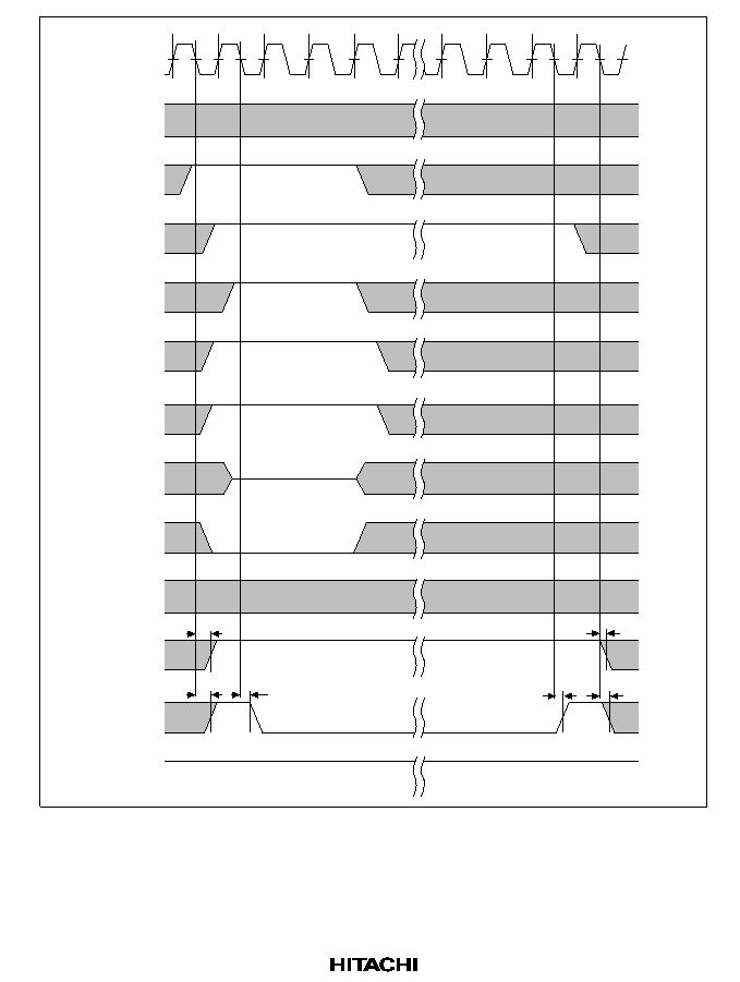
467
CKIO
Address
WAIT
BS
CSn
RD/
WR
,
WE
RD
WEn
,
CASxx
,
DQMxx
DACKn
RAS
,
CE
CKE
D31D0
CAS
,
OE
Tp
Trc
Trc1
Trc2
Trc2
Trc2
Trc1
Tre
t
CED2
t
OED2
t
OED2
t
OED2
t
OED2
t
CED2
Figure 15.65 Pseudo-SRAM Self-Refresh Cycle
(PLL Off, TRP = 1 Cycle, TRAS = 2 Cycles)

468
CKIO
CKIO
BS
CSn
RD/
WR
,
WE
RD
WEn
,
CASxx
,
DQMxx
RAS
,
CE
CAS
,
OE
CKE
D31D0
DACKn
WAIT
T
1
T
W
T
2
T
W
T
2
t
AD
t
BSD
t
CSD1
t
RWD
t
RSD1
t
RWD
t
BSD
t
BSD
t
BSD
t
AD
t
AD
t
CSD2
t
RSD1
t
RDH2
t
RDS1
t
WTS
t
WTH
t
WTS
t
WTH
t
DACD1
t
DACD1
t
DACD2
t
DACD2
t
RDS1
t
RDH2
t
WED1
t
WED1
t
RSD1
t
RSD1
Note:
The DACKn waveform shown is for the case where active-high has been specified.
Figure 15.66 Burst ROM Read Cycle (PLL On, 1 Wait)

469
CKIO
BS
A26A0
CSn
RD/
WR
,
WE
RD
WEn
,
CASxx
,
DQMxx
RAS
,
CE
CAS
,
OE
CKE
D31D0
DACKn
WAIT
T
1
T
W
T
2
T
W
T
2
t
AD
t
BSD
t
RWD
t
RSD2
t
RWD
t
BSD
t
BSD
t
BSD
t
AD
t
AD
t
CSD3
t
RSD2
t
RDH2
t
RDH2
t
RDS2
t
WTS
t
WTH
t
WTS
t
WTH
t
RDS2
t
DACD3
t
DACD1
t
DACD1
t
DACD3
t
WED2
t
RSD2
t
RSD2
t
CSD1
Note:
The DACKn waveform shown is for the case where active-high has been specified.
Figure 15.67 Burst ROM Read Cycle (PLL Off, 1 Wait)

470
T1
T2
t
AD
t
AD
t
IVD
t
RWD
t
IVD
t
RSD1
t
RSD1
t
RDS1
CKIO
A4A0
IVECF
RD/
WR
RD
D7D0
t
RDH7
WAIT
t
WTS
t
WTH
Figure 15.68 Interrupt Vector Fetch Cycle (PLL On, No Waits)

471
T1
T2
t
AD
t
AD
t
IVD
t
RWD
t
IVD
t
RSD2
t
RSD2
t
RDS2
CKIO
A4A0
IVECF
RD/
WR
RD
D7D0
t
RDH7
WAIT
t
WTS
t
WTH
Figure 15.69 Interrupt Vector Fetch Cycle (PLL Off, No Waits)

472
A4A0
CKI0
RD/
WR
WAIT
D7D0
RD
IVECF
T
1
T
W
T
2
t
WTH
t
WTS
t
WTH
t
WTS
Figure 15.70 Interrupt Vector Fetch Cycle (1 External Wait Cycle)
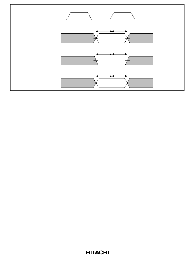
473
t
ASIN
t
AHIN
t
BSS
t
BSH
t
RWS
t
RWH
CKIO
A26A2
RD/
WR
BS
Figure 15.71 Address Monitor Cycle
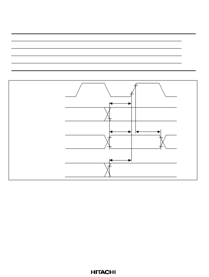
474
15.3.4
DMAC Timing
Table 15.10
DMAC Timing (Conditions: V
CC
= 5.0 V
±
10%, Ta = 20 to +75
°
C)
Item
Symbol Min
Max Unit Figure
DREQ0, DREQ1 setup time (PLL Off, On)
t
DRQS
30
--
ns
15.72
DREQ0, DREQ1 setup time (PLL On, 1/4 cycle delay) t
DRQS
30 1/4 tcyc --
ns
DREQ0, DREQ1 hold time (PLL Off, On)
t
DRQH
15
--
ns
DREQ0, DREQ1 hold time (PLL On, 1/4 cycle delay)
t
DRQH
1/4 tcyc + 15 --
ns
DREQ0, DREQ1 low level width
t
DRQW
1.5
--
t
cyc
t
DRQH
t
DRQS
t
DRQS
t
DRQS
CKIO
DREQ0, DREQ1
level
DREQ0, DREQ1
edge
DREQ0, DREQ1
level cancellation
Figure 15.72 DREQ0, DREQ1 Input Timing

475
15.3.5
Free-Running Timer Timing
Table 15.11
Free-Running Timer Timing (Conditions: V
CC
= 5.0 V
±
10%, Ta = 20 to
+75
°
C)
Item
Symbol
Min
Max
Unit
Figure
Output compare output delay time
(PLL Off, On)
t
TOCD
--
160
ns
15.73
Output compare output delay time
(PLL On, 1/4 cycle delay)
t
TOCD
--
1/4 tcyc + 160 ns
Input capture input setup time
(PLL Off, On)
t
TICS
80
--
ns
Input capture input setup time
(PLL On, 1/4 cycle delay)
t
TICS
80 1/4 tcyc
--
ns
Timer clock input setup time
(PLL Off, On)
t
TCKS
80
--
ns
15.74
Timer clock input setup time
(PLL On, 1/4 cycle delay)
t
TCKS
80 1/4 tcyc
--
ns
Timer clock pulse width (single edge)
t
TCKWH
4.5
--
t
cyc
Timer clock pulse width (both edges)
t
TCKWL
8.5
--
t
cyc
t
TOCD
t
TICS
CKIO
FTOA,
FTOB
FTI
Figure 15.73 FRT Input/Output Timing
t
TCKS
t
TCKWH
t
TCKWL
CKIO
FTCI
Figure 15.74 FRT Clock Input Timing

476
15.3.6
Watchdog Timer Timing
Table 15.12
Watchdog Timer Timing (Conditions: V
CC
= 5.0 V
±
10%, Ta = 20 to +75
°
C)
Item
Symbol
Min
Max
Unit
Figure
WDTOVF
delay time (PLL Off, On)
t
WOVD
--
70
ns
15.75
WDTOVF
delay time (PLL On, 1/4 cycle
delay)
t
WOVD
--
1/4 tcyc + 70
ns
t
WOVD
t
WOVD
CKIO
WDTOVF
Figure 15.75 Watchdog Timer Output Timing
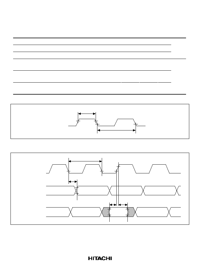
477
15.3.7
Serial Communication Interface Timing
Table 15.13
Serial Communication Interface Timing
(Conditions: V
CC
= 5.0 V
±
10%, Ta = 20 to +75
°
C)
Item
Symbol
Min
Max
Unit
Figure
Input clock cycle
t
scyc
16
--
t
cyc
15.76
Input clock cycle (clocked synchronous mode)
t
scyc
24
--
t
cyc
Input clock pulse width
t
sckw
0.4
0.6
t
scyc
Transmit data delay time (clocked synchronous
mode)
t
TXD
--
70
ns
15.77
Receive data setup time (clocked synchronous
mode)
t
RXS
70
--
ns
Receive data hold time (clocked synchronous
mode)
t
RXH
70
--
ns
t
SCKW
t
scyc
SCK0
Figure 15.76 Input Clock Input/Output Timing
t
scyc
t
TXD
t
RXS
t
RXH
SCK0
TxD0
(transmit data)
RxD0
(receive data)
Figure 15.77 SCI Input/Output Timing (Clocked Synchronous Mode)
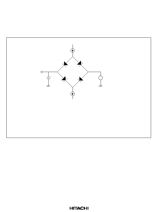
478
15.3.8
AC Characteristics Measurement Conditions
·
I/O signal reference level: 1.5 V
·
Input pulse level: V
SS
to 3.0 V (where RES, NMI, CKIO and MD5-MD0 are within the range
V
SS
to V
CC
)
·
Input rise and fall times: 1 ns
V
I
OH
I
OL
C
L
SH7604
output
pin
DUT output
V
REF
Notes: 1.
2.
C
L
is a total value that includes the capacitance of measurement instruments, etc.,
and is set as follows for each pin.
30 pF: CKIO,
RAS
,
CAS
, CKE,
CS0
CS3
,
BREQ
,
BACK
, DACK0, DACK1,
IVECF
,
CKPACK
.
50 pF: All output pins other than the above.
I
OL
and I
OH
values are as shown in section 15.2, DC Characteristics, and table
15.3, Permitted Output Current Values.
Figure 15.78 Output Load Circuit

479
Section 16 Electrical Characteristics (3V Version)
16.1
Absolute Maximum Ratings
Table 16.1 shows the absolute maximum ratings.
Table 16.1
Absolute Maximum Ratings
Item
Symbol
Rating
Unit
Power supply voltage
V
CC
0.3 to +7.0
V
Input voltage
Vin
0.3 to V
CC
+ 0.3
V
Operating temperature
Topr
20 to +75
°
C
Storage temperature
Tstg
55 to +125
°
C
Caution:
Operating the chip in excess of the absolute maximum rating may result in permanent
damage.

480
16.2
DC Characteristics
Tables 16.2 and 16.3 list DC characteristics.
Table 16.2
DC Characteristics (Conditions: V
CC
= 3.0 to 5.5 V, Ta = 20 to +75
°
C)
Item
Symbol Min
Typ
Max
Unit Test Conditions
Input high-
RES
, NMI,
V
IH
V
CC
×
0.9 --
V
CC
+ 0.3 V
During standby
level
MD5MD0
V
CC
×
0.9 --
V
CC
+ 0.3 V
Normal operation
voltage
EXTAL, CKIO
V
CC
×
0.9 --
V
CC
+ 0.3 V
Other input pins
V
CC
×
0.7 --
V
CC
+ 0.3 V
Input low-
RES
, NMI,
V
IL
0.3
--
V
CC
×
0.1
V
During standby
level
MD5MD0
0.3
--
V
CC
×
0.1
V
Normal operation
voltage
Other input pins
0.3
--
V
CC
×
0.1
V
Input leak
RES
|Iin|
--
--
1.0
µ
A
Vin = 0.5 to V
CC
0.5 V
current
NMI, MD5MD0
--
--
1.0
µ
A
Vin = 0.5 to V
CC
0.5 V
Other input pins
--
--
1.0
µ
A
Vin = 0.5 to V
CC
0.5 V
3-state
leak
current
(while off)
A26A0, D31
D0,
BS
,
CS3
CS0
, RD/
WR
,
RAS
,
CAS
,
WE3
WE0
,
RD
,
IVECF
|I
STI
|
--
--
1.0
µ
A
Vin = 0.5 to V
CC
0.5 V
Output
All output pins
V
OH
V
CC
0.5 --
--
V
I
OH
= 200
µ
A
high-level
voltage
V
CC
1.0 --
--
V
I
OH
= 1 mA
Output low
level
voltage
All output pins
V
OL
--
--
0.4
V
I
OL
= 1.6 mA
Input
RES
Cin
--
--
15
pF
Vin = 0 V
capaci-
NMI
--
--
15
pF
f = 1 MHz
tance
All other input
pins (including
D31D0)
--
--
15
pF
Ta = 25
°
C

481
Table 16.2
DC Characteristics (Conditions: V
CC
= 3.0 to 5.5 V, Ta = 20 to +75
°
C) (cont)
Item
Symbol Min
Typ
Max
Unit Test Conditions
Current
Normal
I
CC
--
25
30
mA
f = 8 MHz
consump-
operation
--
45
55
mA
f = 16 MHz
tion
--
60
70
mA
f = 28.7 MHz
Sleep
--
15
20
mA
f = 8 MHz
--
30
40
mA
f = 16 MHz
--
40
50
mA
f = 28.7 MHz
Standby
--
1
5
µ
A
Ta
50
°
C
--
--
20
µ
A
50
°
C < Ta
Notes: 1. When no PLL is used, do not leave the PLLV
CC
and PLLV
SS
pins open. Connect
PLLV
CC
to V
CC
and PLLV
SS
to V
SS
.
2. Current consumption values shown are the values at which all output pins are without
load under conditions of V
IH
min = V
CC
0.5 V, V
IL
max = 0.5 V.
Table 16.3
Permitted Output Current Values (Conditions: V
CC
= 5.0 V
±
10%, Ta = 20 to
+75
°
C)
Item
Symbol
Min
Typ
Max
Unit
Output low-level permissible current (per pin)
I
OL
--
--
2.0
mA
Output low-level permissible current (total)
I
OL
--
--
80
mA
Output high-level permissible current (per pin)
I
OH
--
--
2.0
mA
Output high-level permissible current (total)
(I
OH
)
--
--
25
mA
Caution:
To ensure chip reliability, do not exceed the output current values given in table 16.3.
482
16.3
AC Characteristics
16.3.1
Clock Timing
Table 16.4
Clock Timing (Conditions: V
CC
= 3.0 to 0.5 V, Ta = 20 to +75
°
C)
Item
Symbol
Min
Max
Unit Figures
Operating frequency
f
OP
4
20
MHz 16.1
Clock cycle time
t
cyc
50
143
*1
or 250
*2
ns
Clock high pulse width
t
CH
8
*1
or 15
*2
--
ns
Clock low pulse width
t
CL
8
*1
or 15
*2
--
ns
Clock rise time
t
CR
--
5
ns
Clock fall time
t
CF
--
5
ns
EXTAL clock input frequency
f
EX
4
8
MHz 16.2
EXTAL clock input cycle time
t
EXcyc
125
250
ns
EXTAL clock input low level pulse width
t
EXL
50
--
ns
EXTAL clock input high level pulse width
t
EXH
50
--
ns
EXTAL clock input rise time
t
EXR
--
5
ns
EXTAL clock input clock fall time
t
EXF
--
5
ns
Power-on oscillation settling time
t
OSC1
10
--
ms
16.3
Software standby oscillation settling time 1
t
OSC2
10
--
ms
16.4
Software standby oscillation settling time 2
t
OSC3
10
--
ms
16.5
PLL synchronization settling time
t
PLL
1
--
µ
s
16.6
Notes: 1. With PLL circuit 1 operating.
2. With PLL circuit 1 not used.
t
CH
1/2 V
CC
t
CF
t
CR
1/2 V
CC
V
IH
CKIO
(input)
V
IH
V
IH
V
IL
V
IL
t
CL
t
cyc
Figure 16.1 CKIO Input Timing
483
EXTAL
(input)
1/2 V
CC
t
EXcyc
t
EXL
t
EXH
t
EXF
t
EXR
V
IH
V
IH
V
IL
V
IL
V
IH
1/2 V
CC
Note:
External clock input from EXTAL pin.
Figure 16.2 EXTAL Clock Input Timing
CKIO,
internal clock
V
CC
V
CC
min
RES
t
OSC1
t
RESW
Stable oscillation
Note:
Oscillation settling time when on-chip crystal oscillator is used.
Figure 16.3 Oscillation Settling Time at Power-On
484
CKIO,
internal
clock
Stable oscillation
Standby
period
t
OSC2
t
RESW
RES
Note:
Oscillation settling time when on-chip crystal oscillator is used.
Figure 16.4 Oscillation Settling Time at Standby Return (via
RES)
CKIO,
internal
clock
Stable oscillation
Standby
period
t
OSC3
NMI
Note:
Oscillation settling time when on-chip crystal oscillator is used.
Figure 16.5 Oscillation Settling Time at Standby Return (via NMI)

485
Stable
oscillation
Stable
oscillation
Oscillation frequency
modification
t
PLL
PLL
synchronization
PLL
synchronization
EXTAL
or CKIO
Internal
clock
Figure 16.6 PLL Synchronization Settling Time

486
16.3.2
Control Signal Timing
Table 16.5
Control Signal Timing (Conditions: V
CC
= 3.0 to 5.5 V, Ta = 20 to +75
°
C)
Item
Symbol Min
Max
Unit
Figure
RES
rise, fall
t
RESr
,
t
RESf
--
200
ns
16.7
RES
pulse width
t
RESW
20
--
t
cyc
NMI reset setup time
t
NMIRS
tcyc + 10
--
ns
NMI reset hold time
t
NMIRH
tcyc + 10
--
ns
NMI rise, fall
t
NMIr
,
t
NMIf
--
200
ns
NMI minimum pulse width
t
IRQES
3
--
tcyc
RES
setup time
*
t
RESS
40
--
ns
16.8,
NMI setup time
*
t
NMIS
40
--
ns
16.9
IRL3
IRL0
setup time
*
t
IRLS
40
--
ns
RES
hold time
t
RESH
20
--
ns
16.8,
NMI hold time
t
NMIH
20
--
ns
16.9
IRL3
IRL0
hold time
t
IRLH
20
--
ns
BRLS
setup time 1 (PLL on)
t
BLSS1
1/2 tcyc + 20 --
ns
16.10
BRLS
hold time 1 (PLL on)
t
BLSH1
15 1/2 tcyc --
ns
BGR
delay time 1 (PLL on)
t
BGRD1
--
1/2 tcyc + 25 ns
BRLS
setup time 1 (PLL on, 1/4 cycle delay) t
BLSS1
1/4 tcyc + 20 --
ns
16.10
BRLS
hold time 1 (PLL on, 1/4 cycle delay)
t
BLSH1
15 1/4 tcyc --
ns
BGR
delay time 1 (PLL on, 1/4 cycle delay)
t
BGRD1
--
3/4 tcyc + 25 ns
BRLS
setup time 2 (PLL off)
t
BLSS2
20
--
ns
16.11
BRLS
hold time 2 (PLL off)
t
BLSH2
30
--
ns
BGR
delay time 2 (PLL off)
t
BGRD2
--
40
ns
Note:
The
RES
, NMI and
IRL3
-
IRL0
signals are asynchronous inputs, but when the setup times
shown here are observed, the signals are considered to have changed at clock fall. If the
setup times are not observed, recognition may be delayed until the next clock fall.

487
Table 16.5
Control Signal Timing (cont)
(Conditions: V
CC
= 3.0 to 5.5 V, Ta = 20 to +75
°
C)
Item
Symbol Min
Max
Unit
Figure
BREQ
delay time 1 (PLL on)
t
BRQD1
--
1/2 tcyc + 25 ns
16.12
BACK
setup time 1 (PLL on)
t
BAKS1
1/2 tcyc + 20 --
ns
BACK
hold time 1 (PLL on)
t
BAKH1
15 1/2 tcyc --
ns
BREQ
delay time 1 (PLL on, 1/4 cycle delay) t
BRQD1
--
3/4 tcyc + 25 ns
16.12
BACK
setup time 1 (PLL on, 1/4 cycle delay) t
BAKS1
1/4 tcyc + 20 --
ns
BACK
hold time 1 (PLL on, 1/4 cycle delay)
t
BAKH1
15 1/4 tcyc --
ns
BREQ
delay time 2 (PLL off)
t
BRQD2
--
40
ns
16.13
BACK
setup time 2 (PLL off)
t
BAKS2
20
--
ns
BACK
hold time 2 (PLL off)
t
BAKH2
30
--
ns
Bus tri-state delay time 1 (PLL on)
t
BOFF1
0
35
ns
16.10,
Bus buffer on time 1 (PLL on)
t
BON1
0
33
ns
16.12
Bus tri-state delay time 1 (PLL on, 1/4 cycle
delay)
t
BOFF1
1/4 tcyc
1/4 tcyc + 35 ns
16.10,
Bus buffer on time 1 (PLL on, 1/4 cycle delay) t
BON1
1/4 tcyc
1/4 tcyc + 33 ns
16.12
Bus tri-state delay time 1 (PLL off)
t
BOFF1
0
45
ns
16.11,
Bus buffer on time 1 (PLL off)
t
BON1
0
40
ns
16.13
Bus tri-state delay time 2 (PLL on)
t
BOFF2
1/2 tcyc
1/2 tcyc + 35 ns
16.10,
Bus buffer on time 2 (PLL on)
t
BON2
1/2 tcyc
1/2 tcyc + 33 ns
16.12
Bus tri-state delay time 2 (PLL on, 1/4 cycle
delay)
t
BOFF2
3/4 tcyc
3/4 tcyc + 35 ns
16.10,
Bus buffer on time 2 (PLL on, 1/4 cycle delay) t
BON2
3/4 tcyc
3/4 tcyc + 33 ns
16.12
Bus tri-state delay time 3 (PLL off)
t
BOFF3
0
45
ns
16.11,
Bus buffer on time 3 (PLL off)
t
BON3
0
40
ns
16.13

488
t
NMIRS
t
RESW
t
RESf
t
RESr
t
NMIRH
RES
NMI
V
IH
V
IL
V
IH
V
IL
V
IH
V
IL
V
IH
V
IL
Figure 16.7 Reset Input Timing
t
RESS
CKIO
RES
t
INMIS
NMI
t
IRLS
IRL3
IRL0
t
RESH
t
NMIH
t
IRLH
V
IH
V
IL
V
IH
V
IL
V
IH
V
IL
Figure 16.8 Interrupt Signal Input Timing (PLL1 Off)

489
CKIO
RES
t
RESH
t
RESS
V
IH
V
IL
NMI
t
NMIH
t
NMIS
V
IH
V
IL
IRL3
IRL0
t
IRLH
t
IRLS
V
IH
V
IL
1/2 t
cyc
or 3/4 t
cyc
1/2 t
cyc
or 3/4 t
cyc
Figure 16.9 Interrupt Signal Input Timing (PLL1 On)
t
BLSS1
CKIO
BRLS
(input)
BGR
(output)
RD
, RD/
WR
,
RAS
,
CAS
,
CSn
,
WEn
,
BS
,
IVECF
A26A0
D31D0
t
BOFF2
t
BOFF1
t
BLSH1
t
BGRD1
t
BLSS1
t
BLSH1
t
BON2
t
BON1
t
BGRD1
Figure 16.10 Bus Release Timing (Master Mode, PLL1 On)

490
A26A0
D31D0
RD
, RD/
WR
,
RAS
,
CAS
,
CSn
,
WEn
,
BS
,
IVECF
BRLS
(input)
BGR
(output)
t
BLSS2
CKIO
t
BOFF1
t
BON1
t
BON3
t
BOFF3
t
BGRD2
t
BGRD2
t
BLSH2
t
BLSS2
t
BLSH2
Figure 16.11 Bus Release Timing (Master Mode, PLL1 Off)
BACK
(input)
RD
, RD/
WR
,
RAS
,
CAS
,
CSn
,
WEn
,
BS
,
IVECF
A26A0
D31D0
BREQ
(output)
t
BAKH1
CKIO
t
BRQD1
t
BRQD1
t
BAKH1
t
BAKS1
t
BON2
t
BON1
t
BOFF1
t
BOFF2
t
BAKS1
Figure 16.12 Bus Release Timing (Slave Mode, PLL1 On)

491
BACK
(input)
RD
, RD/
WR
,
RAS
,
CAS
,
CSn
,
WEn
,
BS
,
IVECF
A26A0
D31D0
BREQ
(output)
CKIO
t
BRQD2
t
BRQD1
t
BAKH2
t
BAKS2
t
BON3
t
BON1
t
BOFF1
t
BOFF3
t
BAKH2
t
BAKS2
Figure 16.13 Bus Release Timing (Slave Mode, PLL1 Off)

492
16.3.3
Bus Timing
Table 16.6
Bus Timing With PLL On [Mode 0, 4]
(Conditions: V
CC
= 3.0 to 5.5 V, Ta = 20 to +75
°
C)
Item
Symbol
Min
Max
Unit
Figures
Address delay time
t
AD
--
28
ns
16.14, 16.20, 16.40,
16.52, 16.66, 16.68
BS
delay time
t
BSD
--
25
ns
16.14, 16.20, 16.40,
16.52, 16.66
CS
delay time 1
t
CSD1
--
25
ns
16.14, 16.20, 16.40,
16.52, 16.66
CS
delay time 2
t
CSD2
--
1/2 tcyc + 25 ns
16.14, 16.66
Read/write delay time
t
RWD
--
25
ns
16.14, 16.20, 16.40,
16.52, 16.66
Read strobe delay time 1
t
RSD1
--
1/2 tcyc + 25 ns
16.14, 16.40, 16.52,
16.66, 16.68
Read data setup time 1
t
RDS1
1/2 tcyc + 10 --
ns
16.14, 16.40, 16.52,
16.66, 16.68
Read data setup time 3
(SDRAM)
t
RDS3
1/2 tcyc + 10 --
ns
16.20
Read data hold time 2
t
RDH2
0
--
ns
16.14, 16.66
Read data hold time 4
(SDRAM)
t
RDH4
0
--
ns
16.20
Read data hold time 5
(DRAM)
t
RDH5
0
--
ns
16.40
Read data hold time 6
(PSRAM)
t
RDH6
0
--
ns
16.52
Read data hold time 7
(interrupt vector)
t
RDH7
0
--
ns
16.68
Write enable delay time
t
WED1
1/2 tcyc + 3
1/2 tcyc + 25 ns
16.14, 16.15, 16.52,
16.53
Write data delay time 1
t
WDD
--
25
ns
16.15, 16.27, 16.41,
16.53
Write data hold time 1
t
WDH1
3
--
ns
16.15, 16.27, 16.41,
16.53
Data buffer on time
t
DON
--
25
ns
16.15, 16.27, 16.41,
16.53
Data buffer off time
t
DOF
--
25
ns
16.15, 16.27, 16.41,
16.53

493
Table 16.6
Bus Timing With PLL On [Mode 0, 4] (cont)
(Conditions: V
CC
= 3.0 to 5.5 V, Ta = 20 to +75
°
C)
Item
Symbol
Min
Max
Unit
Figures
DACK delay time 1
t
DACD1
--
25
ns
16.14, 16.20, 16.40,
16.52, 16.66
DACK delay time 2
t
DACD2
--
1/2 tcyc + 25 ns
16.14, 16.20, 16.40,
16.52, 16.66
WAIT
setup time
t
WTS
20
--
ns
16.19, 16.43, 16.55,
16.66, 16.70
WAIT
hold time
t
WTH
10
--
ns
16.19, 16.43, 16.55,
16.66, 16.70
RAS
delay time 1 (SDRAM) t
RASD1
--
25
ns
16.20
RAS
delay time 2 (DRAM)
t
RASD2
1/2 tcyc + 3
1/2 tcyc + 25 ns
16.40
CAS
delay time 1 (SDRAM) t
CASD1
--
25
ns
16.20
CAS
delay time 2 (DRAM)
t
CASD2
1/2 tcyc + 3
1/2 tcyc + 25 ns
16.40
DQM delay time
t
DQMD
--
25
ns
16.20
CKE delay time
t
CKED
--
33
ns
16.37
CE
delay time 1
t
CED1
1/2 tcyc + 3
1/2 tcyc + 25 ns
16.52
OE
delay time 1
t
OED1
--
1/2 tcyc + 25 ns
16.52
IVECF
delay time
t
IVD
--
25
ns
16.68
Address input setup time
t
ASIN
25
--
ns
16.71
Address input hold time
t
AHIN
10
--
ns
16.71
BS
input setup time
t
BSS
25
--
ns
16.71
BS
input hold time
t
BSH
10
--
ns
16.71
Read/write input setup time
t
RWS
25
--
ns
16.71
Read/write input hold time
t
RWH
10
--
ns
16.71

494
Table 16.7
Bus Timing With PLL On and 1/4 Cycle Delay [Mode 1, 5]
(Conditions: V
CC
= 3.0 to 5.5 V, Ta = 20 to +75
°
C)
Item
Symbol
Min
Max
Unit
Figures
Address delay time
t
AD
--
1/4 tcyc + 28 ns
16.14, 16.20, 16.40,
16.52, 16.66, 16.68
BS
delay time
t
BSD
--
1/4 tcyc + 25 ns
16.14, 16.20, 16.40,
16.52, 16.66
CS
delay time 1
t
CSD1
--
1/4 tcyc + 25 ns
16.14, 16.20, 16.40,
16.52, 16.66
CS
delay time 2
t
CSD2
--
3/4 tcyc + 25 ns
16.14, 16.66
Read/write delay time
t
RWD
--
1/4 tcyc + 25 ns
16.14, 16.20, 16.40,
16.52, 16.66
Read strobe delay time 1
t
RSD1
--
3/4 tcyc + 25 ns
16.14, 16.40, 16.52,
16.66, 16.68
Read data setup time 1
t
RDS1
1/4 tcyc + 10 --
ns
16.14, 16.40, 16.52,
16.66, 16.68
Read data setup time 3
(SDRAM)
t
RDS3
1/4 tcyc + 10 --
ns
16.20
Read data hold time 2
t
RDH2
0
--
ns
16.14, 16.66
Read data hold time 4
(SDRAM)
t
RDH4
0
--
ns
16.20
Read data hold time 5
(DRAM)
t
RDH5
0
--
ns
16.40
Read data hold time 6
(PSRAM)
t
RDH6
0
--
ns
16.52
Read data hold time 7
(interrupt vector)
t
RDH7
0
--
ns
16.68
Write enable delay time
t
WED1
3/4 tcyc + 3
3/4 tcyc + 25 ns
16.14, 16.15, 16.52,
16.53
Write data delay time 1
t
WDD
--
1/4 tcyc + 25 ns
16.15, 16.27, 16.41,
16.53
Write data hold time 1
t
WDH1
1/4 tcyc + 3
--
ns
16.15, 16.27, 16.41,
16.53
Data buffer on time
t
DON
--
1/4 tcyc + 25 ns
16.15, 16.27, 16.41,
16.53
Data buffer off time
t
DOF
--
1/4 tcyc + 25 ns
16.15, 16.27, 16.41,
16.53

495
Table 16.7
Bus Timing With PLL On and 1/4 Cycle Delay [Mode 1, 5] (cont)
(Conditions: V
CC
= 3.0 to 5.5 V, Ta = 20 to +75
°
C)
Item
Symbol
Min
Max
Unit
Figures
DACK delay time 1
t
DACD1
--
1/4 tcyc + 25 ns
16.14, 16.20, 16.40,
16.52, 16.66
DACK delay time 2
t
DACD2
--
3/4 tcyc + 25 ns
16.14, 16.20, 16.40,
16.52, 16.66
WAIT
setup time
t
WTS
20 1/4 tcyc
--
ns
16.19, 16.43, 16.55,
16.66, 16.70
WAIT
hold time
t
WTH
1/4 tcyc+10
--
ns
16.19, 16.43, 16.55,
16.66, 16.70
RAS
delay time 1 (SDRAM) t
RASD1
--
1/4 tcyc + 25 ns
16.20
RAS
delay time 2 (DRAM)
t
RASD2
3/4 tcyc + 3
3/4 tcyc + 25 ns
16.40
CAS
delay time 1 (SDRAM) t
CASD1
--
1/4 tcyc + 25 ns
16.20
CAS
delay time 2 (DRAM)
t
CASD2
3/4 tcyc + 3
3/4 tcyc + 25 ns
16.40
DQM delay time
t
DQMD
--
1/4 tcyc + 25 ns
16.20
CKE delay time
t
CKED
--
1/4 tcyc + 33 ns
16.37
CE
delay time 1
t
CED1
3/4 tcyc + 3
3/4 tcyc + 25 ns
16.52
OE
delay time 1
t
OED1
--
3/4 tcyc + 25 ns
16.52
IVECF
delay time
t
IVD
--
1/4 tcyc + 25 ns
16.68
Address input setup time
t
ASIN
25 1/4 tcyc --
ns
16.71
Address input hold time
t
AHIN
1/4 tcyc+10
--
ns
16.71
BS
input setup time
t
BSS
25 1/4 tcyc --
ns
16.71
BS
input hold time
t
BSH
1/4 tcyc +10
--
ns
16.71
Read/write input setup time
t
RWS
25 1/4 tcyc --
ns
16.71
Read/write input hold time
t
RWH
1/4 tcyc +10
--
ns
16.71

496
Table 16.8
Bus Timing With PLL Off (CKIO Input) [Mode 6]
(Conditions: V
CC
= 3.0 to 5.5 V, Ta = 20 to +75
°
C)
Item
Symbol
Min
Max
Unit
Figures
Address delay time
t
AD
--
43
ns
16.16, 16.38, 16.47,
16.60, 16.67, 16.69
BS
delay time
t
BSD
--
40
ns
16.16, 16.38, 16.47,
16.60, 16.67
CS
delay time 1
t
CSD1
--
40
ns
16.16, 16.38, 16.47,
16.60, 16.67
CS
delay time 3
t
CSD3
--
40
ns
16.16, 16.67
Read write delay time
t
RWD
--
40
ns
16.16, 16.38, 16.47,
16.60, 16.67
Read strobe delay time 2
t
RSD2
--
40
ns
16.16, 16.47, 16.60,
16.67, 16.69
Read data setup time 2
t
RDS2
10
--
ns
16.16, 16.38, 16.47,
16.60, 16.67, 16.69
Read data hold time 2
t
RDH2
0
--
ns
16.16, 16.67
Read data hold time 3
t
RDH3
30
--
ns
16.38
Read data hold time 5
(DRAM)
t
RDH5
0
--
ns
16.47
Read data hold time 6
(PSRAM)
t
RDH6
0
--
ns
16.60
Read data hold time 7
(interrupt vector)
t
RDH7
0
--
ns
16.69
Write enable delay time 2
t
WED2
--
40
ns
16.17, 16.61
Write data delay time
t
WDD
--
40
ns
16.17, 16.39, 16.48,
16.61
Write data hold time 1
t
WDH1
3
ns
16.17, 16.39, 16.48,
16.61
Write data hold time 2
t
WDH2
5
ns
16.17
Write data hold time 3
t
WDH3
3
ns
16.61
DACK delay time 1
t
DACD1
--
40
ns
16.16, 16.38, 16.47,
16.60, 16.67
DACK delay time 3
t
DACD3
--
40
ns
16.16, 16.38, 16.47,
16.60, 16.67

497
Table 16.8
Bus Timing With PLL Off (CKIO Input) [Mode 6] (cont)
(Conditions: V
CC
= 3.0 to 5.5 V, Ta = 20 to +75
°
C)
Item
Symbol
Min
Max
Unit
Figures
WAIT
setup time
t
WTS
20
--
ns
16.19, 16.43, 16.55,
16.67, 16.70
WAIT
hold time
t
WTH
25
--
ns
16.19, 16.43, 16.55,
16.67, 16.70
RAS
delay time 1 (SDRAM) t
RASD1
--
40
ns
16.38
RAS
delay time 3 (DRAM)
t
RASD3
--
40
ns
16.47
CAS
delay time 1 (SDRAM) t
CASD1
--
40
ns
16.38
CAS
delay time 3 (DRAM)
t
CASD3
--
40
ns
16.47
DQM delay time
t
DQMD
--
40
ns
16.38
CKE delay time
t
CKED
--
48
ns
16.37
CE
delay time 2
t
CED2
--
40
ns
16.60
OE
delay time 2
t
OED2
--
40
ns
16.60
IVECF
delay time
t
IVD
--
40
ns
16.69
WE
setup time
t
WES1
0
--
ns
16.16
Address setup time 1
t
AS1
0
--
ns
16.17
Address setup time 2
t
AS2
3
--
ns
16.60
Address hold time 2
t
AH2
0
--
ns
16.17
Row address setup time
t
ASR
3
--
ns
16.47
Column address setup time
t
ASC
3
--
ns
16.47
Write command setup time
t
WCS
3
--
ns
16.48
Write data setup time
t
WDS
3
--
ns
16.48
Address input setup time
*
t
ASIN
20
--
ns
16.71
Address input hold time
*
t
AHIN
25
--
ns
16.71
BS
input setup time
*
t
BSS
20
--
ns
16.71
BS
input hold time
*
t
BSH
25
--
ns
16.71
Read/write input setup time
*
t
RWS
20
--
ns
16.71
Read/write input hold time
*
t
RWH
25
--
ns
16.71
Data buffer on time
t
DON
--
40
ns
16.17, 16.39, 16.48,
16.61
Data buffer off time
t
DOF
--
40
ns
16.17, 16.39, 16.48,
16.61
Note:
When the external addresses monitor function is used, the PLL must be on.

498
Table 16.9
Bus Timing With PLL Off (CKIO Output) [Mode 2]
(Conditions: V
CC
= 3.0 to 5.5 V, Ta = 20 to +75
°
C)
Item
Symbol
Min
Max
Unit
Figures
Address delay time
t
AD
--
28
ns
16.16, 16.38, 16.47,
16.60, 16.67, 16.69
BS
delay time
t
BSD
--
25
ns
16.16, 16.38, 16.47,
16.60, 16.67
CS
delay time 1
t
CSD1
--
25
ns
16.16, 16.38, 16.47,
16.60, 16.67
CS
delay time 3
t
CSD3
--
25
ns
16.16, 16.67
Read write delay time
t
RWD
--
25
ns
16.16, 16.38, 16.47,
16.60, 16.67
Read strobe delay time 2
t
RSD2
--
25
ns
16.16, 16.47, 16.60,
16.67, 16.69
Read data setup time 2
t
RDS2
10
--
ns
16.16, 16.38, 16.47,
16.60, 16.67, 16.69
Read data hold time 2
t
RDH2
0
--
ns
16.16, 16.67
Read data hold time 3
(SDRAM)
t
RDH3
1/2 tcyc
--
ns
16.38
Read data hold time 5
(DRAM)
t
RDH5
0
--
ns
16.47
Read data hold time 6
(PSRAM)
t
RDH6
0
--
ns
16.60
Read data hold time 7
(interrupt vector)
t
RDH7
0
--
ns
16.69
Write enable delay time 2
t
WED2
3
25
ns
16.17, 16.61
Write data delay time
t
WDD
--
25
ns
16.17, 16.39, 16.48,
16.61
Write data hold time 1
t
WDH1
3
--
ns
16.17, 16.39, 16.48,
16.61
Write data hold time 2
t
WDH2
5
--
ns
16.17
Write data hold time 3
t
WDH3
3
--
ns
16.61
DACK delay time 1
t
DACD1
--
25
ns
16.16, 16.38, 16.47,
16.60, 16.67
DACK delay time 3
t
DACD3
--
25
ns
16.16, 16.38, 16.47,
16.60, 16.67

499
Table 16.9
Bus Timing With PLL Off (CKIO Output) [Mode 2] (cont)
(Conditions: V
CC
= 3.0 to 5.5 V, Ta = 20 to +75
°
C)
Item
Symbol
Min
Max
Unit
Figures
WAIT
setup time
t
WTS
20
--
ns
16.19, 16.43, 16.55,
16.67, 16.70
WAIT
hold time
t
WTH
10
--
ns
16.19, 16.43, 16.55,
16.67, 16.70
RAS
delay time 1 (SDRAM) t
RASD1
--
25
ns
16.38
RAS
delay time 3 (DRAM)
t
RASD3
3
25
ns
16.47
CAS
delay time 1 (SDRAM) t
CASD1
--
25
ns
16.38
CAS
delay time 3 (DRAM)
t
CASD3
3
25
ns
16.47
DQM delay time
t
DQMD
--
25
ns
16.38
CKE delay time
t
CKED
--
33
ns
16.37
CE
delay time 2
t
CED2
3
25
ns
16.60
OE
delay time 2
t
OED2
--
25
ns
16.60
IVECF
delay time
t
IVD
--
25
ns
16.69
Address input setup time
*
t
ASIN
25
--
ns
16.71
Address input hold time
*
t
AHIN
10
--
ns
16.71
BS
input setup time
*
t
BSS
25
--
ns
16.71
BS
input hold time
*
t
BSH
10
--
ns
16.71
Read/write input setup time
*
t
RWS
25
--
ns
16.71
Read/write input hold time
*
t
RWH
10
--
ns
16.71
Data buffer on time
t
DON
--
25
ns
16.17, 16.39, 16.48,
16.61
Data buffer off time
t
DOF
--
25
ns
16.17, 16.39, 16.48,
16.61
Note:
When the external addresses monitor function is used, the PLL must be on.
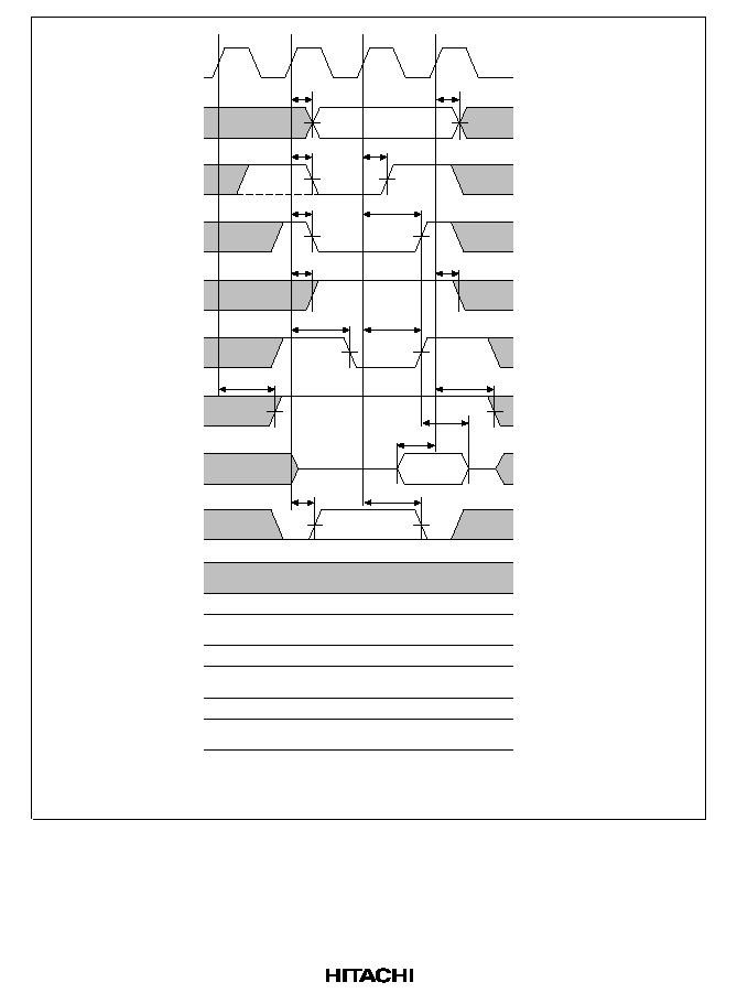
500
CKIO
BS
CSn
RD/
WR
,
WE
RD
WEn
,
CASxx
,
DQMxx
RAS
,
CE
CAS
,
OE
CKE
D31D0
DACKn
WAIT
A26A0
T
1
T
2
t
AD
t
BSD
t
BSD
t
AD
t
CSD1
t
RWD
t
RWD
t
WED1
t
RDS1
t
RDH2
t
WED1
t
CSD2
t
RSD1
t
RSD1
t
DACD1
t
DACD2
Notes: 1.
2.
3.
The dotted line shows the waveform when synchronous DRAM is connected.
t
RDH2
is specified from the rise of
CSn
or
RD
, whichever is first.
The DACKn waveform shown is for the case where active-high has been specified.
Figure 16.14 Basic Read Cycle (No Waits, PLL On)

501
CKIO
BS
CSn
RD/
WR
,
WE
RD
WEn
,
CASxx
,
DQMxx
RAS
,
CE
CAS
,
OE
CKE
D31D0
DACKn
WAIT
A26A0
T
1
T
2
t
AD
t
BSD
t
BSD
t
AD
t
CSD1
t
RWD
t
RWD
t
RSD1
t
RSD1
t
CSD2
t
WED1
t
WED1
t
AH1
t
DACD1
t
DACD2
t
DON
t
WDH1
t
WDD
t
DOF
Notes: 1.
2.
The dotted line shows the waveform when synchronous DRAM is connected.
The DACKn waveform shown is for the case where active-high has been
specified.
Figure 16.15 Basic Write Cycle (No Waits, PLL On)

502
CKIO
BS
CSn
RD/
WR
,
WE
RD
WEn
,
CASxx
,
DQMxx
RAS
,
CE
CAS
,
OE
CKE
D31D0
DACKn
WAIT
A26A0
T
1
T
2
t
AD
t
BSD
t
BSD
t
AD
t
CSD1
t
RWD
t
RDS2
t
RDH2
t
CSD3
t
RSD2
t
DACD1
t
DACD3
t
RWD
t
RSD2
t
WES1
Notes: 1.
2.
3.
The dotted line shows the waveform when synchronous DRAM is connected.
t
RDH2
is specified from the rise of
CSn
or
RD
, whichever is first.
The DACKn waveform shown is for the case where active-high has been specified.
Figure 16.16 Basic Read Cycle (No Waits, PLL Off)

503
CKIO
BS
CSn
RD/
WR
,
WE
RD
WEn
,
CASxx
,
DQMxx
RAS
,
CE
CAS
,
OE
CKE
D31D0
DACKn
WAIT
A26A0
T
1
T
2
t
AD
t
BSD
t
BSD
t
AD
t
CSD1
t
RWD
t
RWD
t
RSD2
t
RSD2
t
DACD1
t
DACD3
t
DON
t
WDD
t
AS1
t
CSD3
t
WED2
t
WED2
t
WDH1
t
WDH2
t
DOF
t
AH2
Notes: 1.
2.
The dotted line shows the waveform when synchronous DRAM is connected.
The DACKn waveform shown is for the case where active-high has been specified.
Figure 16.17 Basic Write Cycle (No Waits, PLL Off)
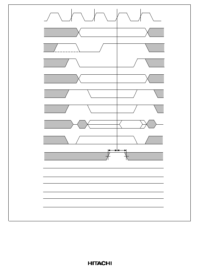
504
T
1
T
w
T
2
CKIO
BS
CSn
RD/
WR
,
WE
RD
WEn
,
CASxx
,
DQMxx
RAS
,
CE
CAS
,
OE
CKE
D31D0
DACKn
WAIT
A26A0
t
WTH
t
WTS
Notes: 1.
2.
The dotted line shows the waveform when synchronous DRAM is connected.
The DACKn waveform shown is for the case where active-high has been specified.
Figure 16.18 Basic Bus Cycle (1 Wait Cycle)

505
T
1
T
w
T
wx
T
2
CKIO
BS
CSn
RD/
WR
,
WE
RD
WEn
,
CASxx
,
DQMxx
RAS
,
CE
CAS
,
OE
CKE
D31D0
DACKn
WAIT
A26A0
t
WTS
t
WTH
t
WTS
t
WTH
Notes: 1.
2.
The dotted line shows the waveform when synchronous DRAM is connected.
The DACKn waveform shown is for the case where active-high has been specified.
Figure 16.19 Basic Bus Cycle (External Wait Input)
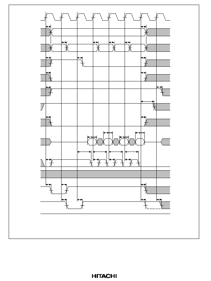
506
CKIO
BS
CSn
RD/
WR
,
WE
RD
WEn
,
CASxx
,
DQMxx
RAS
,
CE
CAS
,
OE
CKE
D31D0
DACKn
WAIT
Upper
address
Lower
address
T
r
T
c
T
d1
T
d2
T
d3
T
d4
t
AD
t
AD
t
AD
t
AD
t
AD
t
AD
t
BSD
t
BSD
t
BSD
t
RWD
t
CSD1
t
CSD1
t
RWD
t
DQMD
t
RDS3
t
DACD2
t
DACD2
t
DACD2
t
DACD2
t
RDH4
t
RDS3
t
RDH4
t
RDS3
t
RDH4
t
RDS3
t
RDH4
t
DACD1
t
DACD1
t
RASD1
t
RASD1
t
RASD1
t
CASD1
t
CASD1
t
CASD1
t
CASD1
t
DACD1
t
DACD1
t
DQMD
t
RSD1
Notes: 1.
2.
The dotted line shows the waveform when synchronous DRAM in another CS space
is accessed.
The DACKn waveform shown is for the case where active-high has been specified.
Figure 16.20 Synchronous DRAM Read Bus Cycle
(RCD = 1 Cycle, CAS Latency = 1 Cycle, Bursts = 4, PLL On)
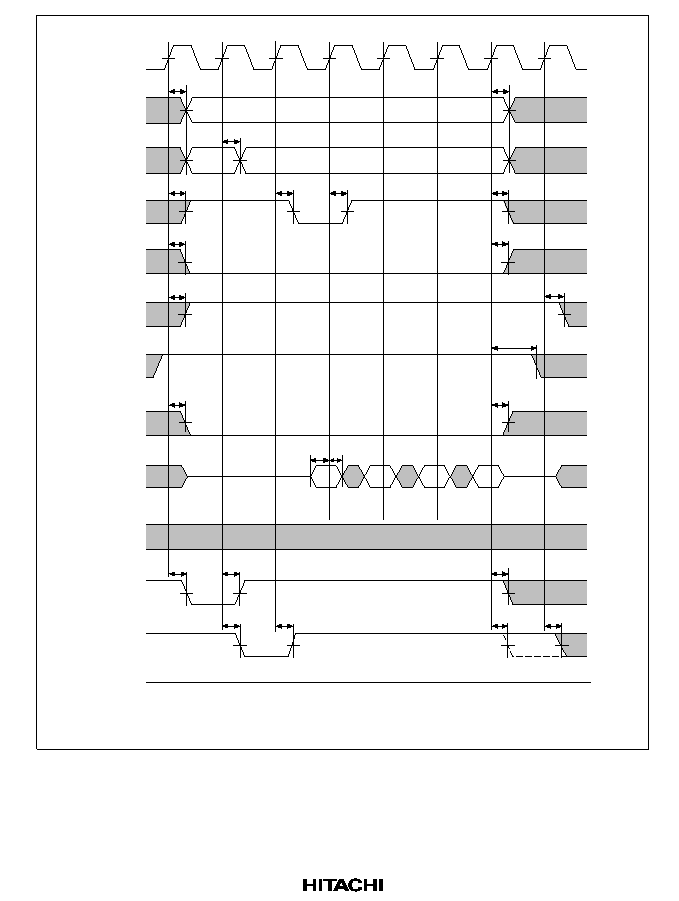
507
CKIO
BS
CSn
RD/
WR
,
WE
RD
WEn
,
CASxx
,
DQMxx
RAS
,
CE
CAS
,
OE
CKE
D31D0
WAIT
Upper
address
Lower
address
T
r
T
c
T
d1
T
d2
T
d3
T
d4
t
AD
t
AD
t
AD
t
BSD
t
BSD
t
BSD
t
BSD
t
RWD
t
CSD1
t
CSD1
t
RWD
t
DQMD
t
RDS3
t
RDH4
t
RASD1
t
RASD1
t
RASD1
t
CASD1
t
CASD1
t
CASD1
t
CASD1
t
DQMD
t
RSD1
Note:
The dotted line shows the waveform when synchronous DRAM in another CS space is
accessed.
Figure 16.21 Synchronous DRAM Single Read Bus Cycle
(RCD = 1 Cycle, CAS Latency = 1 Cycle, Bursts = 4, PLL On)

508
CKIO
BS
CSn
RD/
WR
,
WE
RD
WEn
,
CASxx
,
DQMxx
RAS
,
CE
CAS
,
OE
CKE
D31D0
DACKn
WAIT
Upper
address
Lower
address
T
r
T
rw
T
c
T
w
T
d1
T
d2
T
d3
T
d4
t
BSD
t
RASD1
t
CASD1
t
CASD1
t
RASD1
Notes: 1.
2.
The dotted line shows the waveform when synchronous DRAM in another CS space
is accessed.
The DACKn waveform shown is for the case where active-high has been specified.
Figure 16.22 Synchronous DRAM Read Bus Cycle
(RCD = 2 Cycles, CAS Latency = 2 Cycles, Bursts = 4)
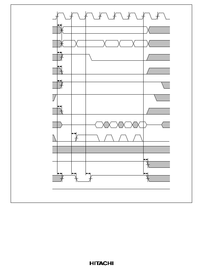
509
CKIO
BS
CSn
RD/
WR
,
WE
RD
WEn
,
CASxx
,
DQMxx
CAS
,
OE
CKE
D31D0
DACKn
WAIT
RAS
,
CE
Upper
address
Lower
address
T
nop
T
c
T
d1
T
d2
T
d3
T
d4
t
AD
t
BSD
t
RWD
t
CSD1
t
DQMD
t
DACD1
t
RASD1
t
CASD1
t
CASD1
t
CASD1
t
CASD1
Note:
The DACKn waveform shown is for the case where active-high has been specified.
Figure 16.23 Synchronous DRAM Read Bus Cycle
(Bank Active, Same Row Access, CAS Latency = 1 Cycle)
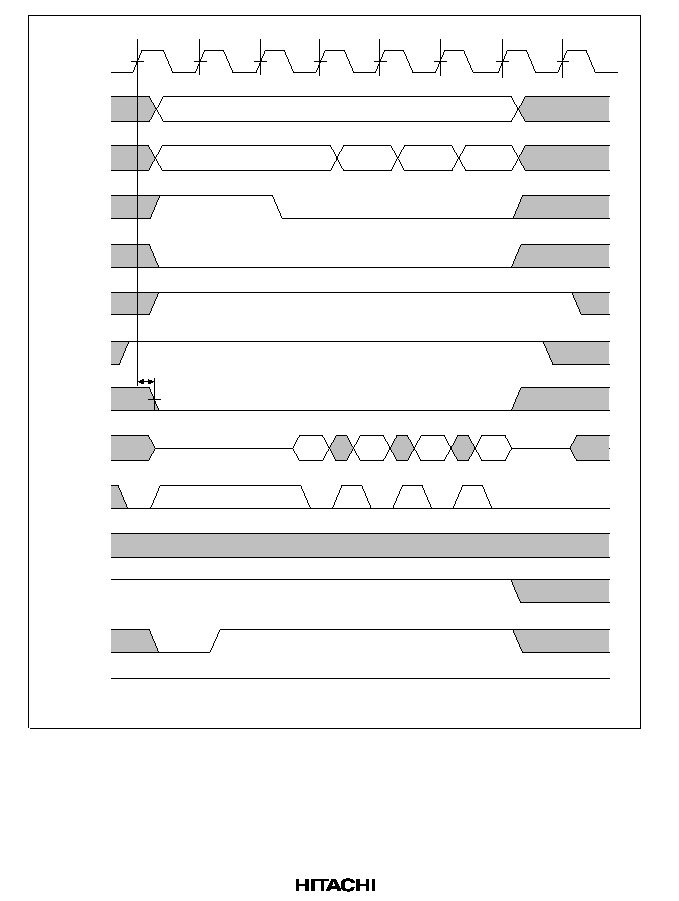
510
Upper
address
Lower
address
BS
CKIO
T
C
T
W
T
d1
T
d2
T
d3
T
d4
CSn
RD/
WR
WE
RD
WEn
CASxx
DQMxx
D31D0
DACKn
WAIT
RAS
CE
CAS
OE
CKE
t
DQMD
Note:
The DACKn waveform shown is for the case where active-high has been specified.
Figure 16.24 Synchronous DRAM Read Bus Cycle
(Bank Active, Same Row Access, CAS Latency = 2 Cycles)
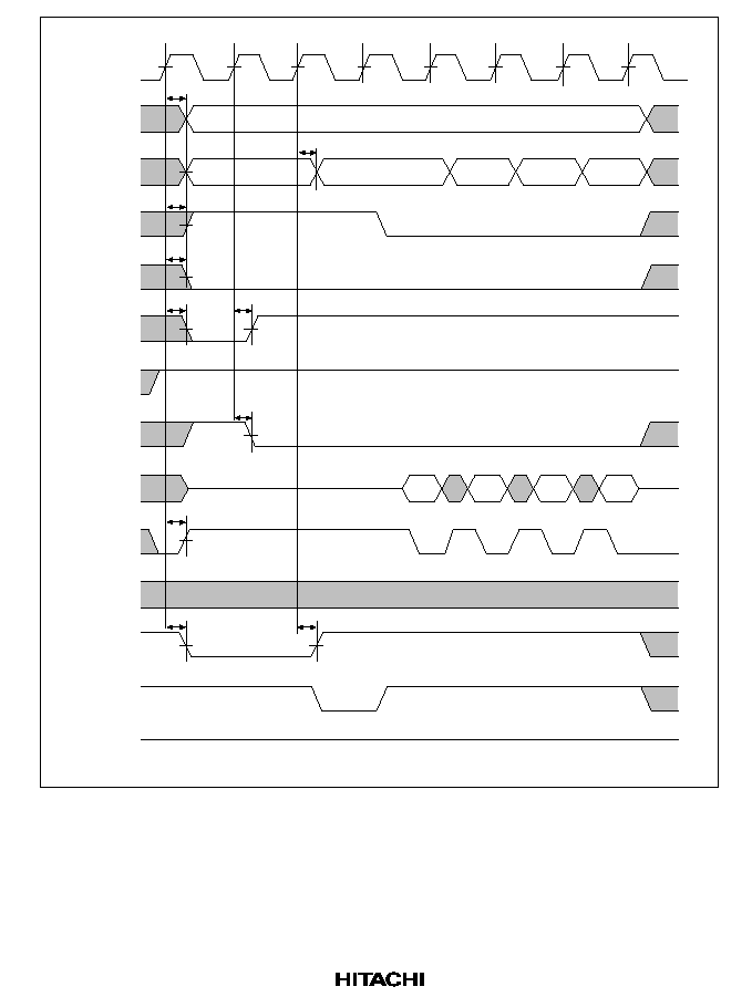
511
Upper
address
Lower
address
BS
CKIO
T
p
T
r
T
c
T
d1
T
d2
T
d3
T
d4
CSn
RD/
WR
WE
RD
WEn
CASxx
DQMxx
D31D0
DACKn
WAIT
RAS
CE
CAS
OE
CKE
t
AD
t
AD
t
BSD
t
CSD1
t
RWD
t
RWD
t
DACD1
t
RASD1
t
RASD1
t
DQMD
Note:
The DACKn waveform shown is for the case where active-high has been specified.
Figure 16.25 Synchronous DRAM Read Bus Cycle (Bank Active, Different Row Access,
TRP = 1 Cycle, RCD = 1 Cycle, CAS Latency = 1 Cycle)
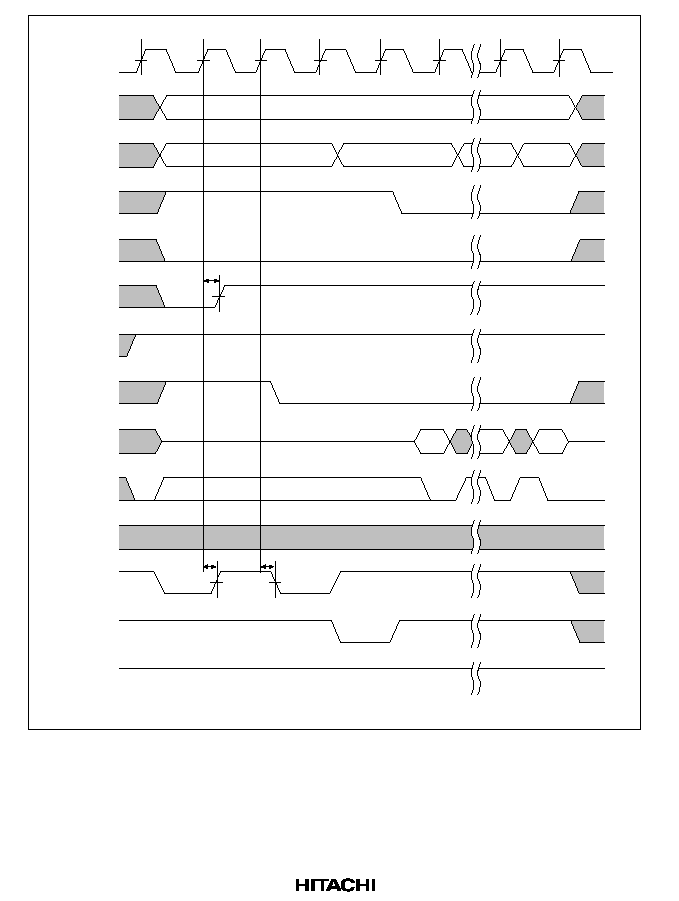
512
Upper
address
Lower
address
BS
CKIO
T
p
T
pw
T
r
T
c
T
d1
T
d4
CSn
RD/
WR
WE
RD
WEn
CASxx
DQMxx
D31D0
DACKn
WAIT
RAS
CE
CAS
OE
CKE
t
RWD
t
RASD1
t
RASD1
Note:
The DACKn waveform shown is for the case where active-high has been specified.
Figure 16.26 Synchronous DRAM Read Bus Cycle (Bank Active, Different Row Access,
TRP = 2 Cycles, RCD = 1 Cycle, CAS Latency = 1 Cycle)
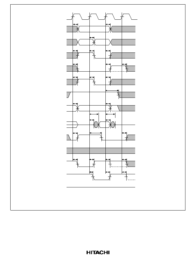
513
CKIO
T
r
T
c
T
ap
Upper
address
WEn
CASxx
DQMxx
D31D0
Lower
address
BS
CSn
RD
RD/
WR
WE
DACKn
WAIT
RAS
CE
CAS
OE
CKE
t
AD
t
AD
t
AD
t
BSD
t
CSD1
t
RWD
t
DQMD
t
DACD1
t
RASD1
t
RASD1
t
CASD1
t
CASD1
t
CASD1
t
RASD1
t
RASD1
t
DQMD
t
DACD1
t
DACD2
t
DON
t
WDD
t
RWD
t
RWD
t
RSD1
t
CSD1
t
CSD1
t
BSD
t
BSD
t
WDH1
Notes: 1.
2.
Dotted lines show the waveforms when synchronous DRAM in another CS space
is accessed.
The DACKn waveform shown is for the case where active-high has been specified.
t
DOF
Figure 16.27 Synchronous DRAM Write Bus Cycle
(RCD = 1 Cycle, TRWL = 1 Cycle, PLL On)

514
Tr
Trw
Tc
Trwl
Tap
CKIO
Upper
address
Lower
address
BS
CSn
RD/
WR
WE
RD
WEn
CASxx
DQMxx
D31D0
DACKn
WAIT
RAS
CE
CAS
OE
CKE
t
RASD1
t
CASD1
t
RASD1
t
DACD1
t
CSD1
Notes: 1.
2.
Dotted lines show the waveforms when synchronous DRAM in another CS space
is accessed.
The DACKn waveform shown is for the case where active-high has been specified.
Figure 16.28 Synchronous DRAM Write Bus Cycle
(RCD = 2 Cycles, TRWL = 2 Cycles)

515
Tc
CKIO
Upper
address
Lower
address
BS
CSn
RD/
WR
WE
RD
WEn
CASxx
DQMxx
D31D0
DACKn
WAIT
RAS
CE
CAS
OE
CKE
t
AD
t
AD
t
BSD
t
BSD
t
CSD1
t
CSD1
t
RWD
t
RWD
t
DQMD
t
DQMD
t
WDD
t
DOF
t
WDH1
t
DON
t
DACD2
t
DACD1
t
RASD1
t
CASD1
t
CASD1
Note:
The DACKn waveform shown is for the case where active-high has been specified.
Figure 16.29 Synchronous DRAM Write Bus Cycle (Bank Active, Same Row Access)

516
Tc
CKIO
Upper
address
Lower
address
BS
CSn
RD/
WR
WE
RD
WEn
CASxx
DQMxx
D31D0
DACKn
WAIT
RAS
CE
CAS
OE
CKE
t
AD
Tc
t
DQMD
t
WDD
t
WDH1
t
DACD2
t
DACD1
t
CASD1
t
CASD1
Note:
The DACKn waveform shown is for the case where active-high has been specified.
Figure 16.30 Synchronous DRAM Consecutive Write Cycles
(Bank Active, Same Row Access)

517
CKIO
Upper
address
Lower
address
BS
CSn
RD/
WR
WE
RD
WEn
CASxx
DQMxx
D31D0
DACKn
WAIT
RAS
CE
CAS
OE
CKE
t
AD
Tp
Tr
Tc
t
BSD
t
CSD1
t
RWD
t
RWD
t
DQMD
t
DQMD
t
DACD1
t
RASD1
t
CASD1
Note:
The DACKn waveform shown is for the case where active-high has been specified.
Figure 16.31 Synchronous DRAM Write Bus Cycle
(Bank Active, Different Row Access, TRP = 1 Cycle, RCD = 1 Cycle)
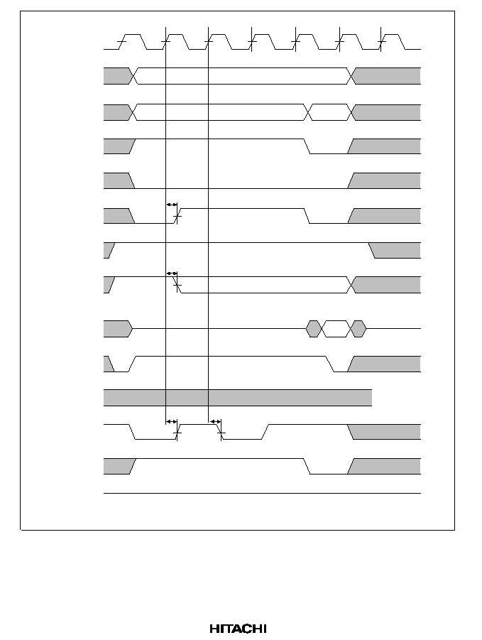
518
Upper
address
Lower
address
BS
CKIO
Tp
T
pw
T
r
T
rw
T
c
CSn
RD/
WR
WE
RD
WEn
CASxx
DQMxx
D31D0
DACKn
WAIT
RAS
CE
CAS
OE
CKE
t
RWD
t
DQMD
t
RASD1
t
RASD1
Note:
The DACKn waveform shown is for the case where active-high has been specified.
Figure 16.32 Synchronous DRAM Write Bus Cycle
(Bank Active, Different Row Access, TRP = 2 Cycles, RCD = 2 Cycles)
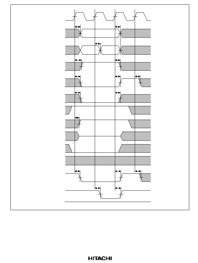
519
CKIO
BS
RD
CSn
RD/
WR
,
WE
WEn
,
CASxx
,
DQMxx
RAS
,
CE
CAS
,
OE
CKE
D31D0
DACKn
WAIT
Upper
address
T
p
T
mw
t
AD
t
BSD
t
AD
Lower
address
t
AD
t
CSD1
t
RWD
t
RWD
t
DQMD
t
CSD1
t
CSD1
t
RASD1
t
RASD1
t
RASD1
t
CSD1
t
CSD1
t
BSD
Figure 16.33 Synchronous DRAM Mode Register Write Cycle (TRP = 1 Cycle)
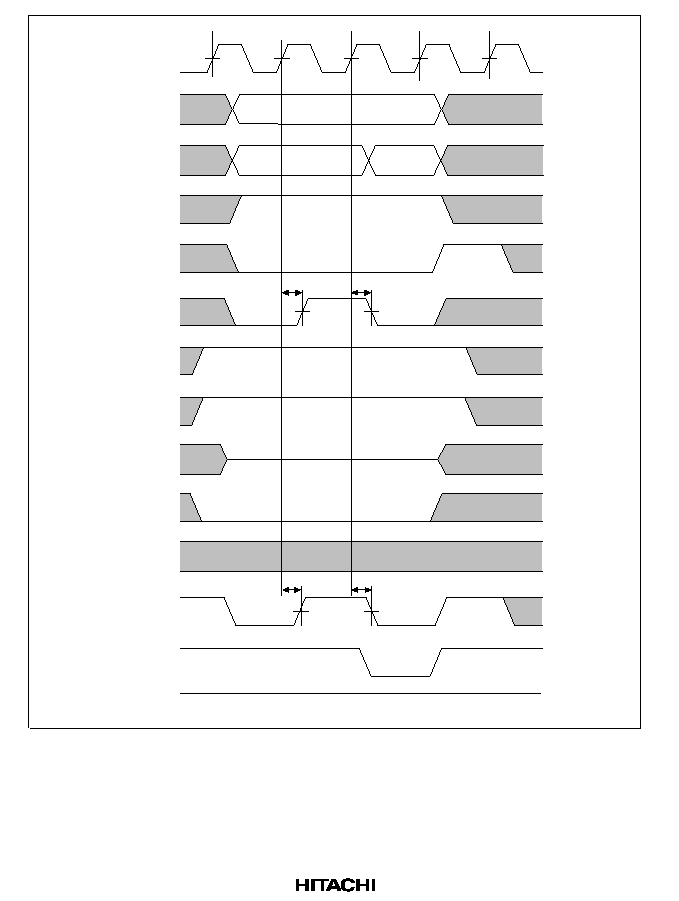
520
CKIO
BS
RD
CSn
RD/
WR
,
WE
WEn
,
CASxx
,
DQMxx
RAS
,
CE
CAS
,
OE
CKE
D31D0
DACKn
WAIT
Upper
address
T
p
T
pw
T
mw
Lower
address
t
RWD
t
RWD
t
RASD1
t
RASD1
Figure 16.34 Synchronous DRAM Mode Register Write Cycle (TRP = 2 Cycles)
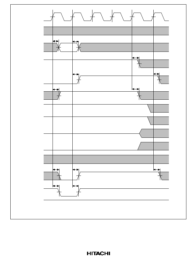
521
CKIO
BS
CSn
RD
RD/
WR
,
WE
WEn
,
CASxx
,
DQMxx
RAS
,
CE
CAS
,
OE
CKE
D31D0
DACKn
WAIT
Upper
address
T
rr
T
rc1
T
re
T
nop
T
rc2
Lower
address
t
RASD1
t
RASD1
t
RASD1
t
CASD1
t
CASD1
t
AD
t
AD
t
CSD1
t
RWD
t
RWD
t
BSD
t
CSD1
Note:
A precharge cycle always precedes the auto-refresh cycle by the number of cycles
specified by TRP.
Figure 16.35 Synchronous DRAM Auto-Refresh Cycle (TRAS = 2 Cycles)
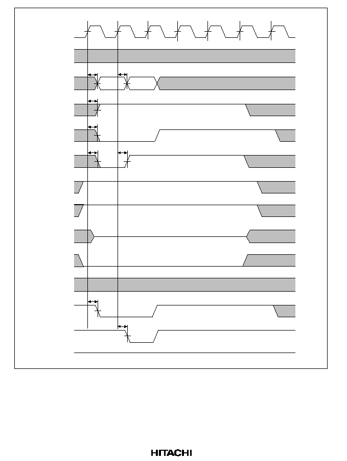
522
CKIO
BS
RD
CSn
RD/
WR
,
WE
WEn
,
CASxx
,
DQMxx
RAS
,
CE
CAS
,
OE
D31D0
DACKn
WAIT
Upper
address
T
p
T
rr
T
rc2
T
re
T
nop
T
rc1
Lower
address
CKE
t
RASD1
t
CASD1
t
AD
t
AD
t
BSD
t
CSD1
t
RWD
t
RWD
Figure 16.36 Synchronous DRAM Auto-Refresh Cycle
(Shown From Precharge Cycle, TRP = 1 Cycle, TRAS = 2 Cycles)

523
Upper
address
Lower
address
BS
CKIO
Trr
T
rc1
T
rc2
T
re
T
rc1
CSn
RD/
WR
WE
WEn
CASxx
DQMxx
D31D0
DACKn
RD
WAIT
RAS
CE
CAS
OE
CKE
Note: A precharge cycle always preceds the self-refresh cycle by the number of cycles specified
by TRP.
t
AD
t
RWD
t
AD
t
RASD1
t
CASD1
t
CKED
t
CKED
t
RASD1
t
CSD1
t
CSD1
T
re
T
nap
t
RASD1
t
CASD1
Figure 16.37 Synchronous DRAM Self-Refresh Cycle (TRAS = 2)
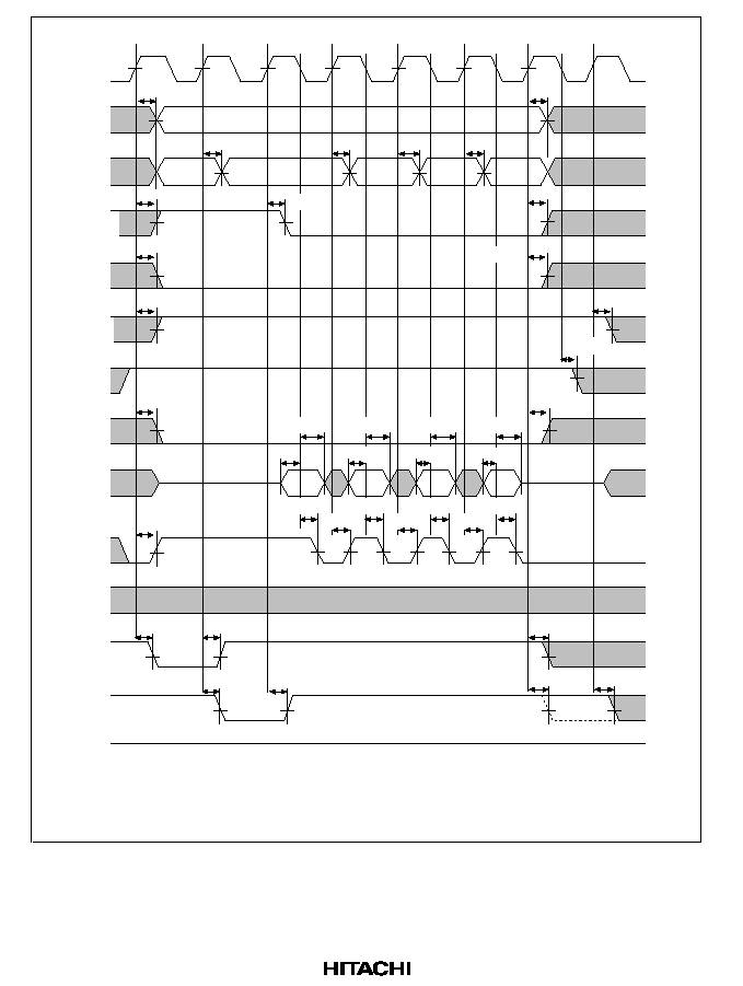
524
Upper
address
Lower
address
BS
CKIO
Tr
T
c
T
d1
T
d2
T
d3
T
d4
CSn
RD/
WR
WE
RD
WEn
CASxx
DQMxx
D31D0
DACKn
WAIT
RAS
CE
CAS
OE
CKE
t
AD
t
AD
t
AD
t
AD
t
AD
t
AD
t
BSD
t
RASD1
t
RASD1
t
RASD1
t
CASD1
t
CSD1
t
RWD
t
DQMD
t
RDS2
t
DACD1
t
DQMD
t
RWD
t
BSD
t
CASD1
t
CASD1
t
CASD1
t
RSD2
t
RDS2
t
RDH3
t
RDH3
t
RDH3
t
RDH3
t
RDS2
t
RDS2
t
DACD3
t
DACD3
t
DACD1
t
DACD1
t
DACD3
t
DACD3
t
DACD1
t
CSD1
t
BSD
Notes: 1.
2.
The dotted line shows the waveform when synchronous DRAM in another CS space
is accessed.
The DACKn waveform shown is for the case where active-high has been specified.
Figure 16.38 Synchronous DRAM Read Bus Cycle
(RCD = 1 Cycle, CAS Latency = 1 Cycle, TRP = 1 Cycle, Bursts = 4, PLL Off)

525
CKIO
T
r
T
c
T
ap
Upper
address
Lower
address
WEn
CASxx
DQMxx
BS
CSn
RD/
WR
WE
RD
D31D0
DACKn
WAIT
RAS
CE
CAS
OE
CKE
t
WDD
t
DON
t
DACD3
t
WDH1
t
DOF
Notes: 1.
2.
Dotted lines show the waveforms when synchronous DRAM in another CS space
is accessed.
The DACKn waveform shown is for the case where active-high has been specified.
Figure 16.39 Synchronous DRAM Write Bus Cycle
(RCD = 1 Cycle, TRWL = 1 Cycle, PLL Off)
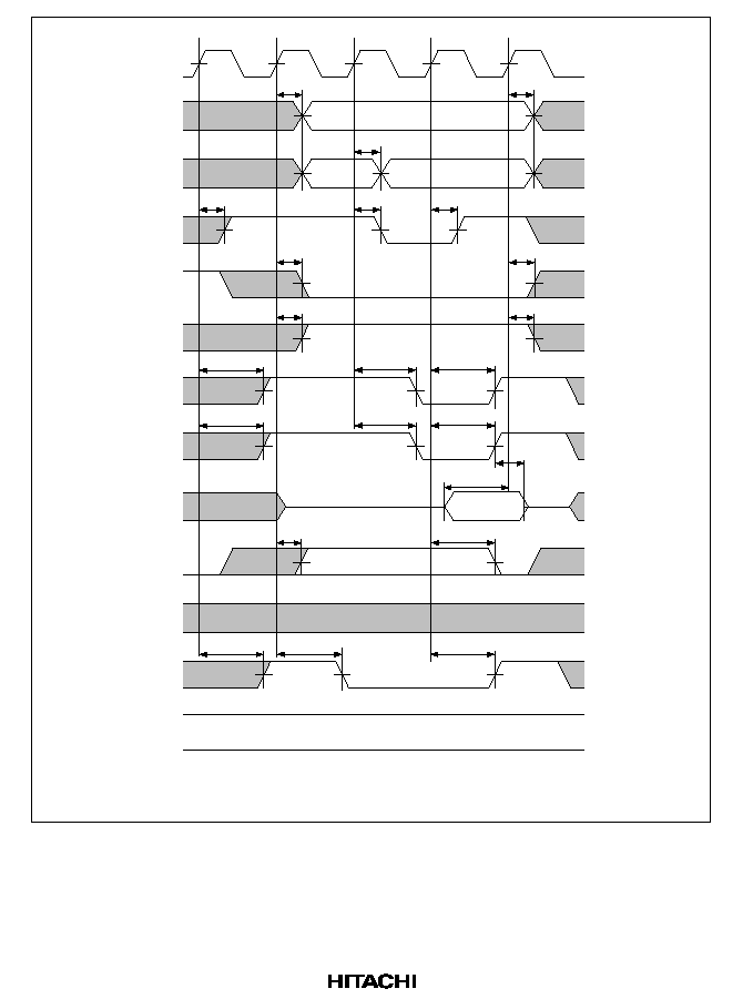
526
CKIO
T
p
T
r
T
c1
T
c2
t
AD
t
AD
t
BSD
t
BSD
t
RDS1
t
DACD2
t
AD
BS
CSn
RD/
WR
,
WE
RD
WEn
,
CASxx
,
DQMxx
RAS
,
CE
CAS
,
OE
CKE
D31D0
DACKn
WAIT
Upper
address
Lower
address
t
BSD
t
RSD1
t
RSD1
t
CASD2
t
CASD2
t
CSD1
t
CSD1
t
RWD
t
RWD
t
CASD2
t
RASD2
t
RASD2
t
RASD2
t
RDH5
t
DACD1
t
RSD1
Notes: 1.
2.
t
RDH5
is specified from the rise of
RD
or
CASxx
, whichever is first.
The DACKn waveform shown is for the case where active-high has been specified.
Figure 16.40 DRAM Read Cycle (TRP = 1 Cycle, RCD = 1 Cycle, No Waits, PLL On)
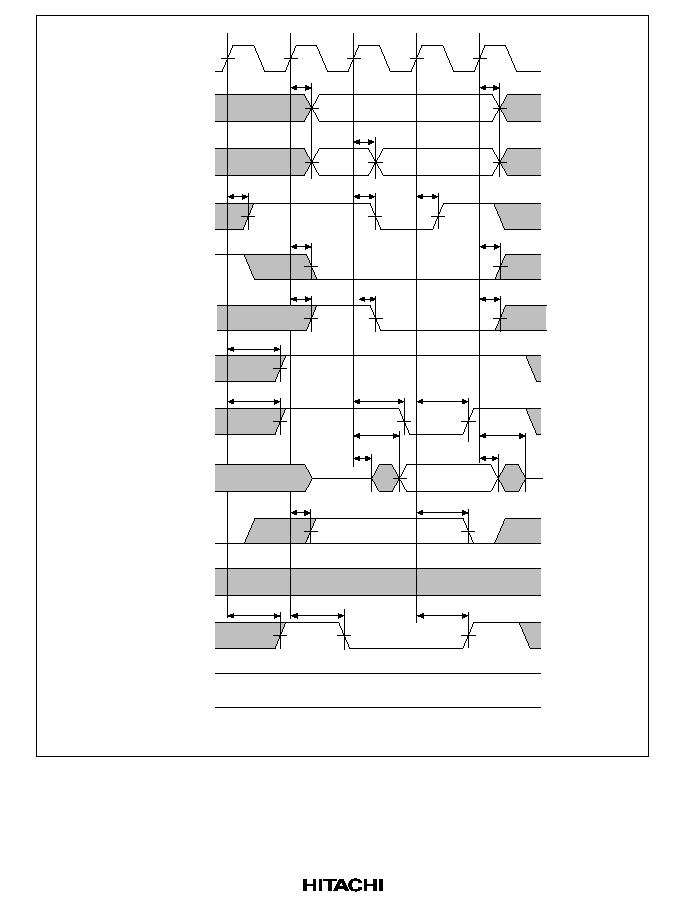
527
CKIO
T
p
T
r
T
c1
T
c2
t
AD
t
AD
t
BSD
t
BSD
t
DACD2
t
AD
BS
CSn
RD/
WR
,
WE
RD
WEn
,
CASxx
,
DQMxx
RAS
,
CE
CAS
,
OE
CKE
D31D0
DACKn
WAIT
Upper
address
Lower
address
t
BSD
t
CASD2
t
CASD2
t
CSD1
t
CSD1
t
RWD
t
RWD
t
CASD2
t
RASD2
t
RASD2
t
RASD2
t
DACD1
t
RSD1
t
RWD
t
DON
t
WDH1
t
WDD
t
DOF
Note:
The DACKn waveform shown is for the case where active-high has been specified.
Figure 16.41 DRAM Write Cycle
(TRP = 1 Cycle, RCD = 1 Cycle, No Waits, PLL On)
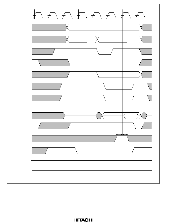
528
CKIO
BS
CSn
RD/
WR
,
WE
RD
WEn
,
CASxx
,
DQMxx
RAS
,
CE
CAS
,
OE
CKE
D31D0
DACKn
WAIT
Upper
address
Lower
address
T
p
T
pw
T
r
T
rw
T
c1
T
c2
T
w
t
WTH
t
WTS
Note:
The DACKn waveform shown is for the case where active-high has been specified.
Figure 16.42 DRAM Bus Cycle (TRP = 2 Cycles, RCD = 2 Cycles, 1 Wait)
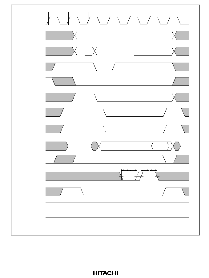
529
CKIO
T
p
T
r
T
c1
T
w
T
wx
T
c2
BS
CSn
RD/
WR
,
WE
RD
WEn
,
CASxx
,
DQMxx
RAS
,
CE
CAS
,
OE
CKE
D31D0
DACKn
WAIT
Upper
address
Lower
address
t
WTS
t
WTH
t
WTS
t
WTH
Note:
The DACKn waveform shown is for the case where active-high has been specified.
Figure 16.43 DRAM Bus Cycle (TRP = 1 Cycle, RCD = 1 Cycle, External Wait Input)

530
CKIO
T
p
T
r
T
c1
T
c2
T
c1
T
c2
t
AD
t
BSD
t
DACD1
BS
RD/
WR
,
WE
RD
WEn
,
CASxx
,
DQMxx
RAS
,
CE
CAS
,
OE
CKE
D31D0
DACKn
WAIT
Upper
address
Lower
address
t
RSD1
t
RSD1
t
CASD2
t
CASD2
t
DACD2
t
RDS1
CSn
t
BSD
t
RDH5
t
RDS1
t
RDH5
Notes: 1.
2.
t
RDH5
is specified from the rise of
RD
or
CASxx
, whichever is first.
The DACKn waveform shown is for the case where active-high has been specified.
Figure 16.44 DRAM Burst Read Cycle
(TRP = 1 Cycle, RCD = 1 Cycle, No Waits, PLL On)

531
CKIO
T
p
T
r
T
c1
T
c2
T
c1
T
c2
t
AD
t
BSD
t
DACD1
BS
CSn
RD/
WR
,
WE
RD
WEn
,
CASxx
,
DQMxx
RAS
,
CE
CAS
OE
CKE
D31D0
DACKn
WAIT
Upper
address
Lower
address
t
WDH1
t
BSD
t
CASD2
t
CASD2
t
WDD
t
DACD2
Note:
The DACKn waveform shown is for the case where active-high has been specified.
Figure 16.45 DRAM Burst Write Cycle
(TRP = 1 Cycle, RCD = 1 Cycle, No Waits, PLL On)
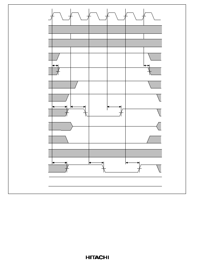
532
CKIO
BS
CSn
RD/
WR
,
WE
RD
WEn
,
CASxx
,
DQMxx
RAS
,
CE
CAS
,
OE
CKE
D31D0
DACKn
WAIT
Upper
address
Lower
address
T
p
t
CSD1
T
rr
T
rc1
T
rc2
T
re
t
CASD2
t
CASD2
t
CASD2
t
RASD2
t
RASD2
t
RASD2
t
CSD1
Figure 16.46 DRAM CAS-Before-RAS Refresh Cycle
(TRP = 1 Cycle, TRAS = 2 Cycles, PLL On)
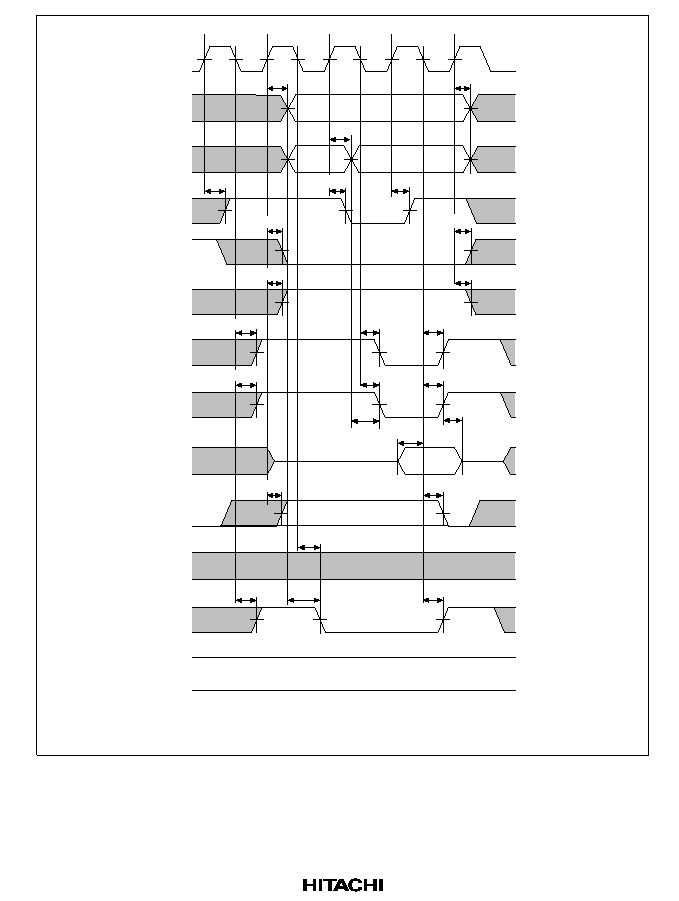
533
CKIO
T
p
T
r
T
c1
T
c2
t
AD
t
AD
t
BSD
t
BSD
t
RDS2
t
DACD3
t
AD
BS
CSn
RD/
WR
,
WE
RD
WEn
,
CASxx
,
DQMxx
RAS
,
CE
CAS
,
OE
CKE
D31D0
DACKn
WAIT
Upper
address
Lower
address
t
BSD
t
RSD2
t
RSD2
t
CASD3
t
CASD3
t
CSD1
t
CSD1
t
RWD
t
RWD
t
CASD3
t
RASD3
t
ASR
t
RASD3
t
ASC
t
RDH5
t
DACD1
t
RASD3
t
RSD2
Notes: 1.
2.
t
RDH5
is specified from the rise of
RD
or
CASxx
, whichever is first.
The DACKn waveform shown is for the case where active-high has been specified.
Figure 16.47 DRAM Read Cycle (TRP = 1 Cycle, RCD = 1 Cycle, No Waits, PLL Off)
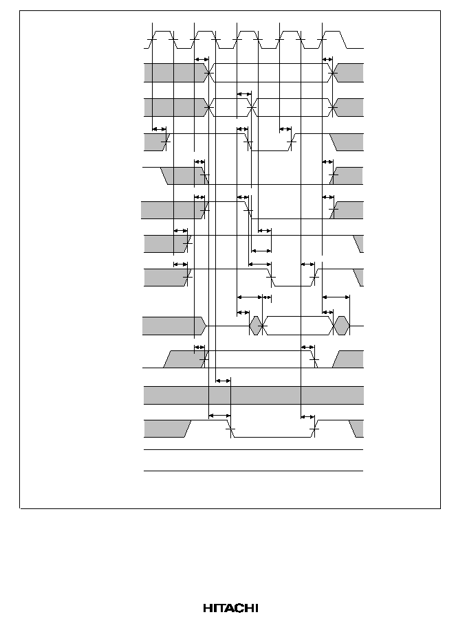
534
CKIO
T
p
T
r
T
c1
T
c2
t
AD
t
AD
t
BSD
t
BSD
t
DON
t
WDH1
t
DACD3
t
AD
BS
CSn
RD/
WR
,
WE
RD
WEn
,
CASxx
,
DQMxx
RAS
,
CE
CAS
,
OE
CKE
D31D0
DACKn
WAIT
Upper
address
Lower
address
t
BSD
t
RSD2
t
CASD3
t
WCS
t
ASC
t
CSD1
t
CSD1
t
RWD
t
RWD
t
CASD3
t
RASD3
t
ASR
t
WDD
t
DOF
t
DACD1
t
RASD3
t
RWD
t
CASD3
t
WDS
Note:
The DACKn waveform shown is for the case where active-high has been specified.
Figure 16.48 DRAM Write Cycle (TRP = 1 Cycle, RCD = 1 Cycle, No Waits, PLL Off)
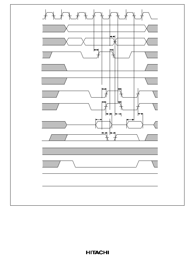
535
CKIO
T
p
T
r
T
c1
T
c2
T
c1
T
c2
t
AD
t
BSD
t
DACD1
BS
CSn
RD/
WR
,
WE
RD
WEn
,
CASxx
,
DQMxx
RAS
,
CE
CAS
,
OE
CKE
D31D0
DACKn
WAIT
Upper
address
Lower
address
t
RDH5
t
RDS2
t
BSD
t
RSD2
t
CASD3
t
CASD3
t
RDH5
t
RDS2
t
DACD3
t
RSD2
t
ASC
Notes: 1.
2.
t
RDH5
is specified from the rise of
RD
or
CASxx
, whichever is first.
The DACKn waveform shown is for the case where active-high has been specified.
Figure 16.49 DRAM Burst Read Cycle
(TRP = 1 Cycle, RCD = 1 Cycle, No Waits, PLL Off)

536
CKIO
T
p
T
r
T
c1
T
c2
T
c1
T
c2
t
AD
t
BSD
t
DACD1
BS
CSn
RD/
WR
,
WE
RD
WEn
,
CASxx
,
DQMxx
RAS
,
CE
CAS
,
OE
CKE
D31D0
DACKn
WAIT
Upper
address
Lower
address
t
BSD
t
CASD3
t
ASC
t
CASD3
t
WDD
t
DACD3
t
WDS
t
WDH1
Note:
The DACKn waveform shown is for the case where active-high has been specified.
Figure 16.50 DRAM Burst Write Cycle
(TRP = 1 Cycle, RCD = 1 Cycle, No Waits, PLL Off)

537
CKIO
BS
CSn
RD/
WR
,
WE
RD
WEn
,
CASxx
,
DQMxx
RAS
,
CE
CAS
,
OE
CKE
D31D0
DACKn
WAIT
Upper
address
Lower
address
T
p
t
CSD1
T
rr
T
rc1
T
rc2
T
re
t
RWD
t
RSD2
t
CASD3
t
CASD3
t
RASD3
t
RASD3
t
CSD1
t
CASD3
t
RASD3
Figure 16.51 DRAM CAS-Before-RAS Refresh Cycle
(TRP = 1 Cycle, TRAS = 2 Cycles, PLL Off)

538
CKIO
T
p
T
r
T
c1
T
c2
t
AD
t
BSD
t
RDS1
t
DACD2
t
AD
BS
CSn
RD/
WR
,
WE
RD
WEn
,
CASxx
,
DQMxx
RAS
,
CE
CAS
,
OE
CKE
D31D0
DACKn
WAIT
Upper
address
t
BSD
t
RSD1
t
RSD1
t
RSD1
t
WED1
t
CSD1
t
CSD1
t
RWD
t
RWD
t
WED1
t
CED1
t
CED1
t
CED1
t
DACD1
t
RSD1
t
OED1
t
OED1
t
OED1
t
RDH6
Note:
The DACKn waveform shown is for the case where active-high has been specified.
Figure 16.52 Pseudo-SRAM Read Cycle
(PLL On, TRP = 1 Cycle, RCD = 1 Cycle, No Waits)
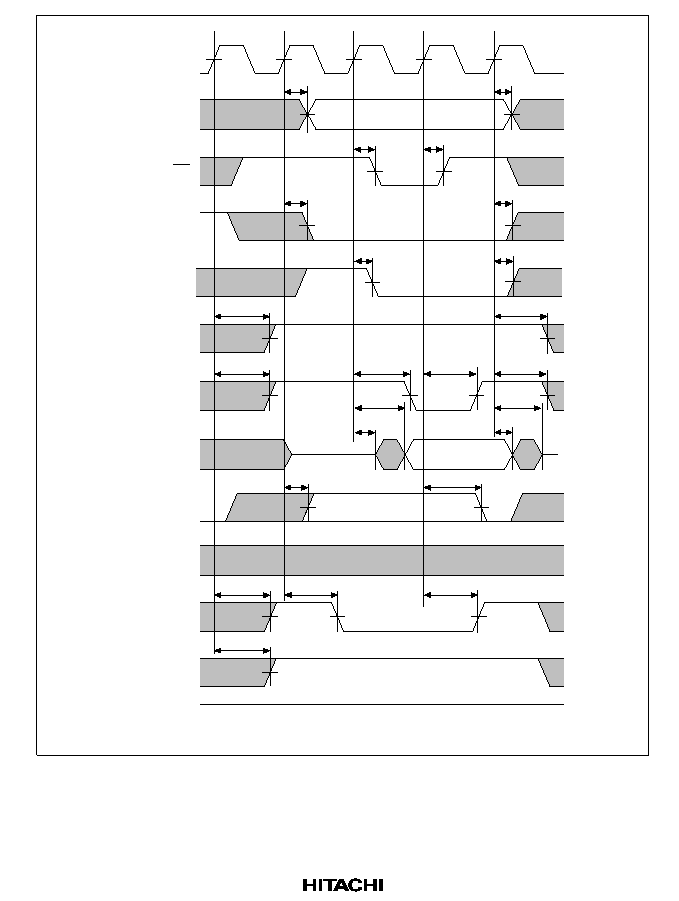
539
CKIO
T
p
T
r
T
c1
T
c2
t
AD
t
BSD
t
DACD2
t
AD
BS
CSn
RD/
WR
,
WE
RD
WEn
,
CASxx
,
DQMxx
RAS
,
CE
CAS
,
OE
CKE
D31D0
DACKn
WAIT
Address
t
BSD
t
WED1
t
WED1
t
WED1
t
RSD1
t
CSD1
t
CSD1
t
RSD1
t
CED1
t
CED1
t
CED1
t
DACD1
t
WED1
t
OED1
t
DOF
t
WDD
t
RWD
t
RWD
t
DON
t
WDH1
Note:
The DACKn waveform shown is for the case where active-high has been specified.
Figure 16.53 Pseudo-SRAM Write Cycle
(PLL On, TRP = 1 Cycle, RCD = 1 Cycle, No Waits)
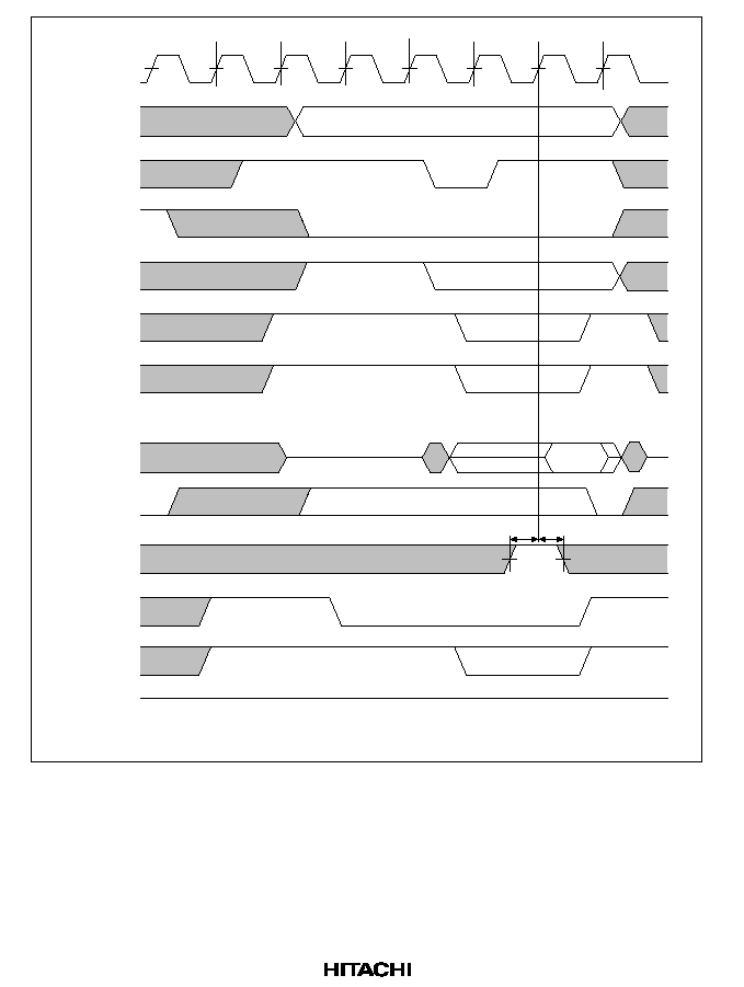
540
CKIO
BS
CSn
RD/
WR
,
WE
RD
WEn
,
CASxx
,
DQMxx
RAS
,
CE
CAS
,
OE
CKE
D31D0
DACKn
WAIT
Address
T
p
T
pw
T
r
T
rw
T
c1
T
c2
T
w
t
WTH
t
WTS
Note:
The DACKn waveform shown is for the case where active-high has been specified.
Figure 16.54 Pseudo-SRAM Bus Cycle (TRP = 2 Cycles, RCD = 2 Cycles, 1 Wait)
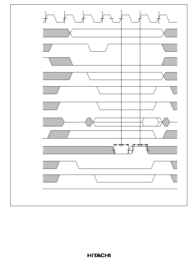
541
CKIO
T
p
T
r
T
c1
T
w
T
wx
T
c2
BS
CSn
RD/
WR
,
WE
RD
WEn
,
CASxx
,
DQMxx
RAS
,
CE
CAS
,
OE
CKE
D31D0
DACKn
WAIT
Address
t
WTS
t
WTH
t
WTS
t
WTH
Note:
The DACKn waveform shown is for the case where active-high has been specified.
Figure 16.55 Pseudo-SRAM Bus Cycle
(TRP = 1 Cycle, RCD = 1 Cycle, External Wait Input)
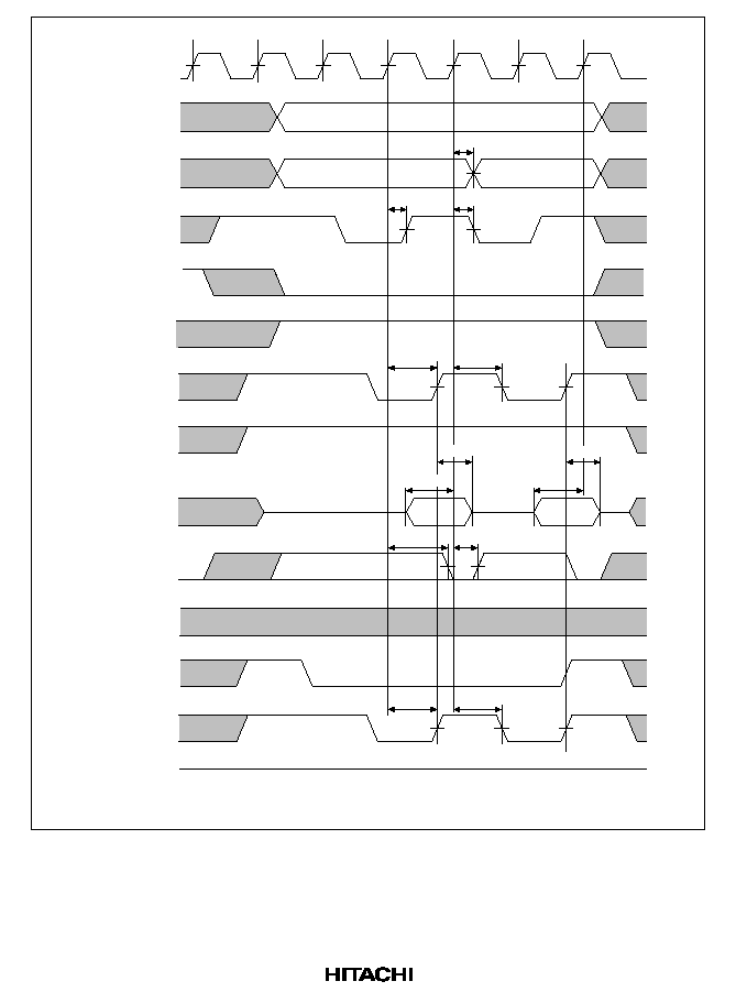
542
CKIO
T
p
T
r
T
c1
T
c2
T
c1
T
c2
t
AD
t
BSD
t
DACD1
BS
RD/
WR
,
WE
RD
WEn
,
CASxx
,
DQMxx
RAS
,
CE
CAS
,
OE
CKE
D31D0
DACKn
WAIT
Upper
address
Lower
address
t
RSD1
t
RSD1
t
OED1
t
OED1
t
DACD2
t
RDS1
CSn
t
BSD
t
RDH6
t
RDS1
t
RDH6
Note:
The DACKn waveform shown is for the case where active-high has been specified.
Figure 16.56 Pseudo-SRAM Read Cycle
(Static Column Mode, PLL On, TRP = 1 Cycle, RCD = 1 Cycle, No Waits)

543
CKIO
T
p
T
r
T
c1
T
c2
T
c1
T
c2
t
AD
t
BSD
t
DACD1
BS
CSn
RD/
WR
,
WE
RD
WEn
,
CASxx
,
DQMxx
RAS
,
CE
CAS
,
OE
CKE
D31D0
DACKn
WAIT
Upper
address
Lower
address
t
BSD
t
WED1
t
WED1
t
WDD
t
DACD2
t
WDH1
Note:
The DACKn waveform shown is for the case where active-high has been specified.
Figure 16.57 Pseudo-SRAM Write Cycle
(Static Column Mode, PLL On, TRP = 1 Cycle, RCD = 1 Cycle, No Waits)

544
CKIO
BS
Address
T
p
T
rr
T
rc1
T
rc2
T
re
WAIT
CSn
RD/
WR
,
WE
RD
D31D0
DACKn
WEn
,
CASxx
,
DQMxx
RAS
,
OE
CAS
,
OE
CKE
t
WED1
t
CED1
t
CED1
t
OED1
t
OED1
t
OED1
t
OED1
t
WED1
Figure 16.58 Pseudo-SRAM Auto-Refresh Cycle
(PLL On, TRP = 1 Cycle, TRAS = 2 Cycles)
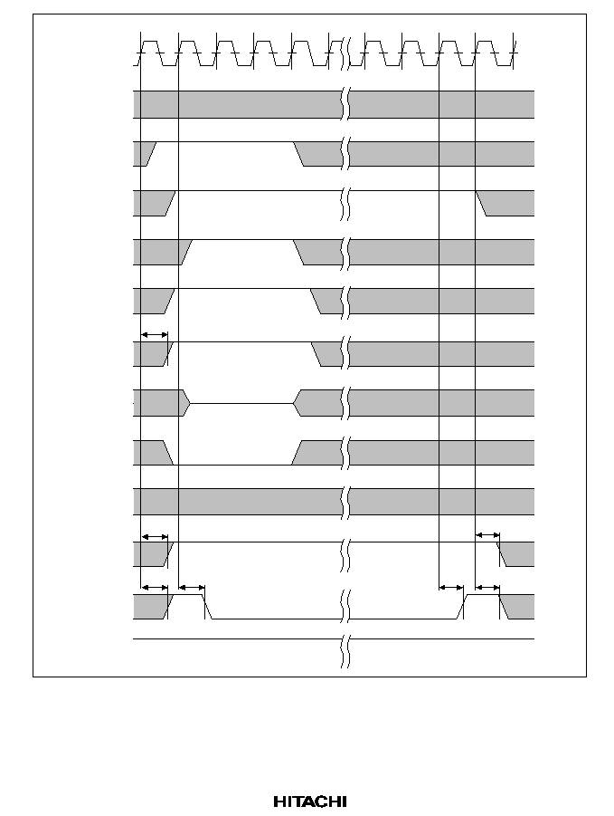
545
CKIO
Address
WAIT
BS
CSn
RD/
WR
,
WE
RD
WEn
,
CASxx
,
DQMxx
DACKn
RAS
,
CE
CKE
D31D0
CAS
,
OE
T
p
T
rc
T
rc1
T
rc2
T
rc1
T
re
t
WED1
t
CED1
t
OED1
t
OED1
t
OED1
t
OED1
t
CED1
Figure 16.59 Pseudo-SRAM Self-Refresh Cycle
(PLL On, TRP = 1 Cycle, TRAS = 2 Cycles)

546
CKIO
Address
T
p
T
r
T
c1
T
c2
BS
CSn
RD/
WR
,
WE
RD
WEn
,
CASxx
,
DQMxx
RAS
,
CE
CKE
D31D0
DACKn
WAIT
CAS
,
OE
t
AD
t
RSD2
t
BSD
t
BSD
t
CSD1
t
RWD
t
AD
t
RSD2
t
RSD2
t
RDH6
t
RDS2
t
OED2
t
CED2
t
AS2
t
CED2
t
CSD1
t
RWD
t
DACD1
t
DACD3
t
OED2
t
CED2
t
OED2
t
WED2
Note:
The DACKn waveform shown is for the case where active-high has been specified.
Figure 16.60 Pseudo-SRAM Read Cycle
(PLL Off, TRP = 1 Cycle, RCD = 1 Cycle, No Waits)
547
CKIO
Address
T
p
T
r
T
c1
T
c2
BS
CSn
RD/
WR
,
WE
RD
WEn
,
CASxx
,
DQMxx
RAS
,
CE
CKE
D31D0
DACKn
WAIT
CAS
,
OE
t
AD
t
RWD
t
BSD
t
BSD
t
CSD1
t
RWD
t
AD
t
WED2
t
WDD
t
DON
t
DOF
t
WDH1
t
CED2
t
CED2
t
AS2
t
CED2
t
OED2
t
CSD1
t
RWD
t
RSD2
t
WED2
t
WED2
t
DACD1
t
DACD3
t
WDH3
Note:
The DACKn waveform shown is for the case where active-high has been specified.
Figure 16.61 Pseudo-SRAM Write Cycle
(PLL Off, TRP = 1 Cycle, RCD = 1 Cycle, No Waits)
548
Upper
address
Lower
address
CKIO
BS
CSn
D31D0
CSn
WAIT
WEn
,
CASxx
DQMxx
RD/
WR
,
WE
RD
CAS
,
OE
CKE
RAS
,
CE
T
p
T
r
T
c1
T
c2
T
c1
T
c2
t
AD
t
BSD
t
BSD
t
RSD2
t
RSD2
t
RDH6
t
RDS2
t
OED2
t
DACD1
t
RDS2
t
RDH6
t
DACD3
t
OED2
Note:
The DACKn waveform shown is for the case where active-high has been specified.
Figure 16.62 Pseudo-SRAM Read Cycle
(Static Column Mode, PLL Off, TRP = 1 Cycle, RCD = 1 Cycle, No Waits)

549
Upper
address
Lower
address
CKIO
BS
CSn
D31D0
DACKn
WAIT
WEn
,
CASxx
,
DQMxx
RD/
WR
,
WE
RD
CAS
,
OE
CKE
RAS
,
CE
T
p
T
r
T
c1
T
c2
T
c1
T
c2
t
AD
t
BSD
t
BSD
t
CSD1
t
RWD
t
WED2
t
DOF
t
WDH1
t
BSD
t
BSD
t
AD
t
WDD
t
WDH1
t
RWD
t
WED2
t
DACD1
t
AD
t
DACD3
t
CED2
t
DON
t
CED2
t
WDD
t
WED2
t
WDH3
t
WDH3
t
DACD1
t
DACD3
t
WED2
t
CSD1
Note:
The DACKn waveform shown is for the case where active-high has been specified.
Figure 16.63 Pseudo-SRAM Write Cycle
(Static Column Mode, PLL Off, TRP = 1 Cycle, RCD = 1 Cycle, No Waits)
550
CKIO
BS
Address
T
p
T
rr
T
rc1
T
rc2
T
re
WAIT
CSn
RD/
WR
,
WE
RD
D31D0
DACKn
WEn
,
CASxx
,
DQMxx
RAS
,
OE
CAS
,
OE
CKE
t
CED2
t
CED2
t
OED2
t
OED2
t
OED2
t
OED2
Figure 16.64 Pseudo-SRAM Auto-Refresh Cycle
(PLL Off, TRP = 1 Cycle, TRAS = 2 Cycles)

551
CKIO
Address
WAIT
BS
CSn
RD/
WR
,
WE
RD
WEn
,
CASxx
,
DQMxx
DACKn
RAS
,
CE
CKE
D31D0
CAS
,
OE
Tp
Trc
Trc1
Trc2
Trc2
Trc2
Trc1
Tre
t
CED2
t
OED2
t
OED2
t
OED2
t
OED2
t
CED2
Figure 16.65 Pseudo-SRAM Self-Refresh Cycle
(PLL Off, TRP = 1 Cycle, TRAS = 2 Cycles)

552
CKIO
CKIO
BS
CSn
RD/
WR
,
WE
RD
WEn
,
CASxx
,
DQMxx
RAS
,
CE
CAS
,
OE
CKE
D31D0
DACKn
WAIT
T
1
T
W
T
2
T
W
T
2
t
AD
t
BSD
t
CSD1
t
RWD
t
RSD1
t
RWD
t
BSD
t
BSD
t
BSD
t
AD
t
AD
t
CSD2
t
RSD1
t
RDH2
t
RDS1
t
WTS
t
WTH
t
WTS
t
WTH
t
DACD1
t
DACD1
t
DACD2
t
DACD2
t
RDS1
t
RDH2
t
WED1
t
WED1
t
RSD1
t
RSD1
Note:
The DACKn waveform shown is for the case where active-high has been specified.
Figure 16.66 Burst ROM Read Cycle (PLL On, 1 Wait)
553
CKIO
BS
A26A0
CSn
RD/
WR
,
WE
RD
WEn
,
CASxx
,
DQMxx
RAS
,
CE
CAS
,
OE
CKE
D31D0
DACKn
WAIT
T
1
T
W
T
2
T
W
T
2
t
AD
t
BSD
t
RWD
t
RSD2
t
RWD
t
BSD
t
BSD
t
BSD
t
AD
t
AD
t
CSD3
t
RSD2
t
RDH2
t
RDH2
t
RDS2
t
WTS
t
WTH
t
WTS
t
WTH
t
RDS2
t
DACD3
t
DACD1
t
DACD1
t
DACD3
t
WED2
t
RSD2
t
RSD2
t
CSD1
Note:
The DACKn waveform shown is for the case where active-high has been specified.
Figure 16.67 Burst ROM Read Cycle (PLL Off, 1 Wait)
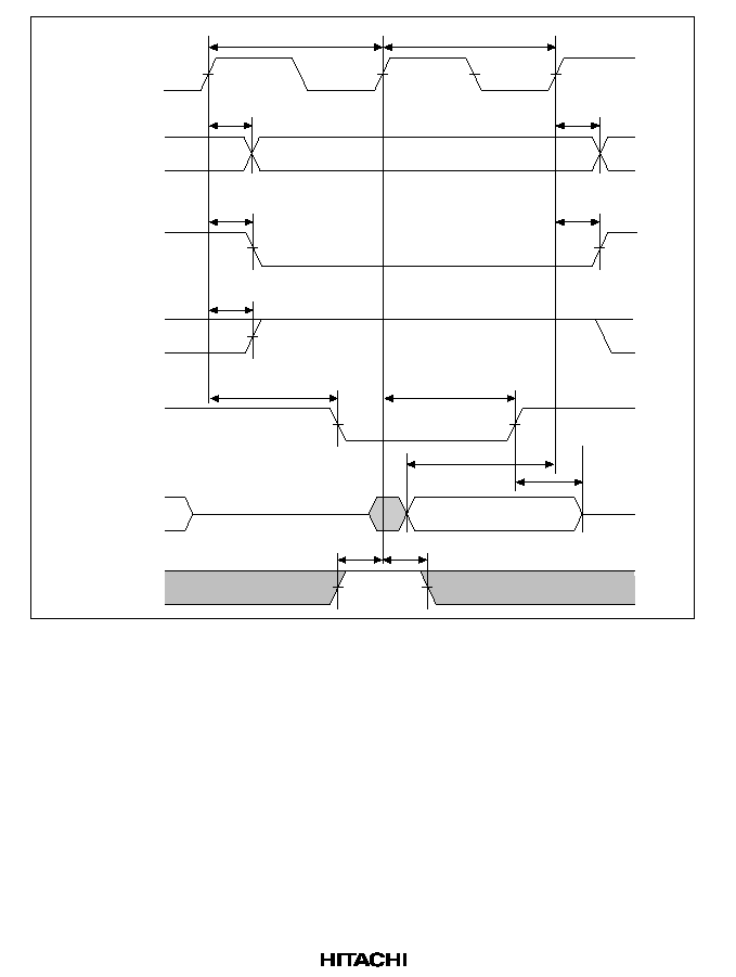
554
T1
T2
t
AD
t
AD
t
IVD
t
RWD
t
IVD
t
RSD1
t
RSD1
t
RDS1
CKIO
A4A0
IVECF
RD/
WR
RD
D7D0
t
RDH7
WAIT
t
WTS
t
WTH
Figure 16.68 Interrupt Vector Fetch Cycle (PLL On, No Waits)
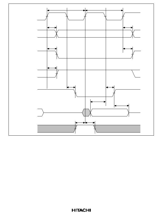
555
T1
T2
t
AD
t
AD
t
IVD
t
RWD
t
IVD
t
RSD2
t
RSD2
t
RDS2
CKIO
A4A0
IVECF
RD/
WR
RD
D7D0
t
RDH7
WAIT
t
WTS
t
WTH
Figure 16.69 Interrupt Vector Fetch Cycle (PLL Off, No Waits)
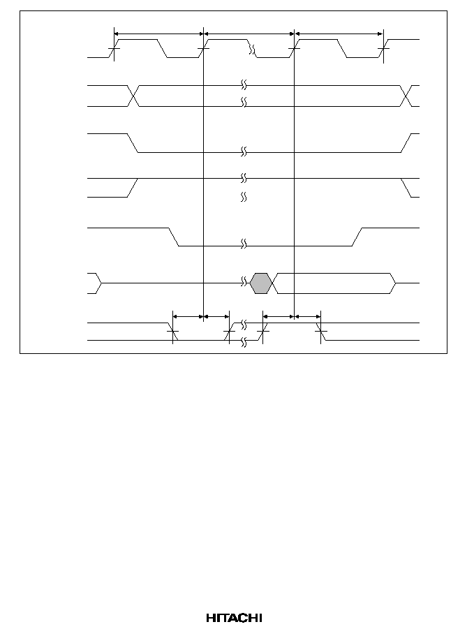
556
A4A0
CKI0
RD/
WR
WAIT
D7D0
RD
IVECF
T
1
T
W
T
2
t
WTH
t
WTS
t
WTH
t
WTS
Figure 16.70 Interrupt Vector Fetch Cycle (1 External Wait Cycle)

557
t
ASIN
t
AHIN
t
BSS
t
BSH
t
RWS
t
RWH
CKIO
A26A2
RD/
WR
BS
Figure 16.71 Address Monitor Cycle

558
16.3.4
DMAC Timing
Table 16.10
DMAC Timing (Conditions: V
CC
= 3.0 to 5.5 V, Ta = 20 to +75
°
C)
Item
Symbol Min
Max Unit Figure
DREQ0, DREQ1 setup time (PLL Off, On)
t
DRQS
50
--
ns
16.72
DREQ0, DREQ1 setup time (PLL On, 1/4 cycle delay) t
DRQS
50 1/4 tcyc --
ns
DREQ0, DREQ1 hold time (PLL Off, On)
t
DRQH
50
--
ns
DREQ0, DREQ1 hold time (PLL On, 1/4 cycle delay)
t
DRQH
1/4 tcyc + 50 --
ns
DREQ0, DREQ1 low level width
t
DRQW
1.5
--
t
cyc
t
DRQH
t
DRQS
t
DRQS
t
DRQS
CKIO
DREQ0, DREQ1
level
DREQ0, DREQ1
edge
DREQ0, DREQ1
level cancellation
Figure 16.72 DREQ0, DREQ1 Input Timing
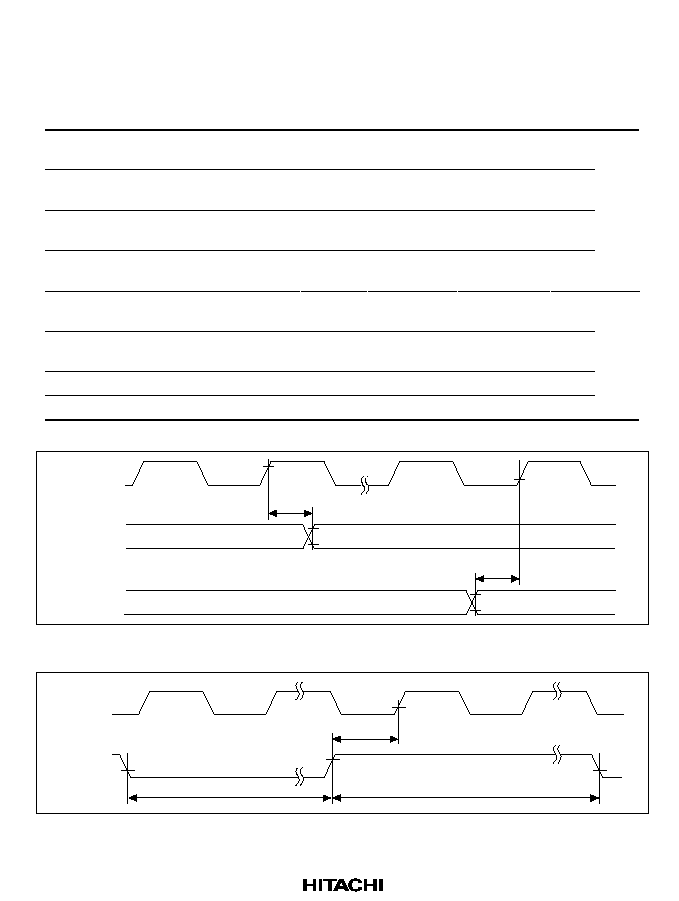
559
16.3.5
Free-Running Timer Timing
Table 16.11
Free-Running Timer Timing (Conditions: V
CC
= 3.0 to 5.5 V, Ta = 20 to
+75
°
C)
Item
Symbol
Min
Max
Unit
Figure
Output compare output delay time
(PLL Off, On)
t
TOCD
--
320
ns
16.73
Output compare output delay time
(PLL On, 1/4 cycle delay)
t
TOCD
--
1/4 tcyc + 320 ns
Input capture input setup time
(PLL Off, On)
t
TICS
80
--
ns
Input capture input setup time
(PLL On, 1/4 cycle delay)
t
TICS
80 1/4 tcyc
--
ns
Timer clock input setup time
(PLL Off, On)
t
TCKS
80
--
ns
16.74
Timer clock input setup time
(PLL On, 1/4 cycle delay)
t
TCKS
80 1/4 tcyc
--
ns
Timer clock pulse width (single edge)
t
TCKWH
4.5
--
t
cyc
Timer clock pulse width (both edges)
t
TCKWL
8.5
--
t
cyc
t
TOCD
t
TICS
CKIO
FTOA,
FTOB
FTI
Figure 16.73 FRT Input/Output Timing
t
TCKS
t
TCKWH
t
TCKWL
CKIO
FTCI
Figure 16.74 FRT Clock Input Timing
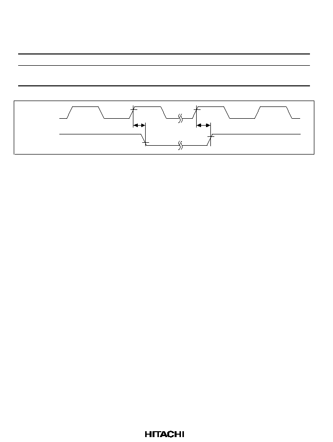
560
16.3.6
Watchdog Timer Timing
Table 16.12
Watchdog Timer Timing (Conditions: V
CC
= 3.0 to 5.5 V, Ta = 20 to +75
°
C)
Item
Symbol
Min
Max
Unit
Figure
WDTOVF
delay time (PLL Off, On)
t
WOVD
--
70
ns
16.75
WDTOVF
delay time (PLL On, 1/4 cycle
delay)
t
WOVD
--
1/4 tcyc + 70
ns
t
WOVD
t
WOVD
CKIO
WDTOVF
Figure 16.75 Watchdog Timer Output Timing

561
16.3.7
Serial Communication Interface Timing
Table 16.13
Serial Communication Interface Timing
(Conditions: V
CC
= 3.0 to 5.5 V, Ta = 20 to +75
°
C)
Item
Symbol
Min
Max
Unit
Figure
Input clock cycle
t
scyc
16
--
t
cyc
16.76
Input clock cycle (clocked synchronous mode)
t
scyc
24
--
t
cyc
Input clock pulse width
t
sckw
0.4
0.6
t
scyc
Transmission data delay time (clocked
synchronous mode)
t
TXD
--
70
ns
16.77
Receive data setup time (clocked synchronous
mode)
t
RXS
70
--
ns
Receive data hold time (clocked synchronous
mode)
t
RXH
70
--
ns
t
SCKW
t
scyc
SCK0
Figure 16.76 Input Clock Input/Output Timing
t
scyc
t
TXD
t
RXS
t
RXH
SCK0
TxD0
(transmit data)
RxD0
(receive data)
Figure 16.77 SCI Input/Output Timing (Clocked Synchronous Mode)

562
16.3.8
AC Characteristics Measurement Conditions
·
I/O signal reference level: 1.5 V
·
Input pulse level: V
SS
to 3.0 V (where RES, NMI, CKIO and MD5-MD0 are within the range
V
SS
to V
CC
)
·
Input rise and fall times: 1 ns
V
I
OH
I
OL
C
L
SH7604
output
pin
DUT output
V
REF
Notes: 1.
2.
C
L
is a total value that includes the capacitance of measurement instruments, etc.,
and is set as follows for each pin.
30 pF: CKIO,
RAS
,
CAS
, CKE,
CS0
CS3
,
BREQ
,
BACK
, DACK0, DACK1,
IVECF
,
CKPACK
.
50 pF: All output pins other than the above.
I
OL
and I
OH
values are as shown in section 16.2, DC Characteristics, and table
16.3, Permitted Output Current Values.
Figure 16.78 Output Load Circuit

563
Appendix A Pin States
Table A.1
Pin States During Resets, Power-Down State, and Bus-Released State
Pin States
Reset
Power-On
Reset
Manual
Power-Down
Modes
Bus-
Category
Pin
Master
Slave
Bus
Acquired
Bus
Released
Standby
Sleep
Released
Mode
Clock
CKIO
IO
*1
IO
*1
IO
*1
IO
*1
IO
*1
IO
*1
IO
*1
EXTAL
I
*1
I
*1
I
*1
I
*1
I
*1
I
*1
I
*1
XTAL
O
*1
O
*1
O
*1
O
*1
O
*1
O
*1
O
*1
CKPREQ
Z
Z
I
I
I
I
I
CKPACK
H
H
H
H
H
*2
H
H
System control
RESET
I
I
I
I
I
I
I
WDTOVF
H
H
H
H
O
O
O
BACK
,
BRLS
Z
Z
I
I
Z
I
I
BREQ,
BGR
H
H
O
O
H
O
O
MD5MD0
I
I
I
I
I
I
I
Interrupt
NMI
I
I
I
I
I
I
I
IRL3
IRL0
Z
Z
Z
Z
I
I
I
IVECF
H
H
H
H
H
*3
H
H
Address bus
A26A0
O
Z
O
Z
Z
O
Z
*4
Data bus
D31D0
Z
Z
IO
Z
Z
Z
Z
Bus control
CS3
CS0
H
Z
O
Z
H
H
Z
*4
BS
H
Z
O
Z
H
H
Z
RD/
WR
H
Z
O
Z
H
H
Z
*4
RAS,
CE
H
Z
O
Z
H
H
Z
CAS
,
OE
H
Z
O
Z
H
H
Z
CASHH
, DQMUU H
Z
O
Z
H
H
Z
CASHL
, DQMUL
H
Z
O
Z
H
H
Z
CASLH
, DQMLU
H
Z
O
Z
H
H
Z
CASLL
, DQMLL
H
Z
O
Z
H
H
Z
RD
H
Z
O
Z
H
H
Z
CKE
H
H
O
H
O
O
H
WAIT
Z
Z
I
Z
Z
I
Ignored

564
Table A.1
Pin States During Resets, Power-Down State, and Bus-Released State (cont)
Pin States
Reset
Power-On
Reset
Manual
Power-Down
Modes
Bus-
Category
Pin
Master
Slave
Bus
Acquired
Bus
Released
Standby
Sleep
Released
Mode
Direct memory
DACK0, DACK1
H
H
H
H
K
*3
O
O
access
controller
(DMAC)
DREQ0, DREQ1
Z
Z
Z
Z
Z
I
I
16-bit free-
FTOA
L
L
L
L
K
*3
O
O
running timer
FTOB
L
L
L
L
K
*3
O
O
(FRT)
FTI
Z
Z
Z
Z
K
*3
I
I
FTCI
Z
Z
Z
Z
K
*3
I
I
Serial
RXD
Z
Z
Z
Z
K
*3
I
I
communication
TXD
H
H
H
H
K
*3
O
O
interface (SCI)
SCK
Z
Z
Z
Z
K
*3
IO
I
I: Input
O: Output
H: High-level output
L: Low-level output
Z: High impedance
K: Input pins are high impedance, output pins retain their state
Notes: 1. Depends on the clock mode (MD2MD0 setting).
2. Low-level output in standby mode when the clock is paused.
3. When the high impedance bit (HIZ) in the standby control register (SBYCR) is set to 1,
output pins become high impedance.
4. Input when the external bus cycle address monitor function is used.
Other: In sleep mode, if the DMAC is running, the address/data bus and bus control signals
change according to the DMAC operation (the same applies during refreshing).

565
Appendix B List of Registers
B.1
List of I/O Registers
Abbrevia-
tion of
Bit Name
Address
Register
Bit 7
Bit 6
Bit 5
Bit 4
Bit 3
Bit 2
Bit 1
Bit 0
Module
H'FFFFFE00
SMR
C/
A
CHR
PE
O/
E
STOP
MP
CKS1
CKS0
SCI
H'FFFFFE01
BRR
H'FFFFFE02
SCR
TIE
RIE
TE
RE
MPIE
TEIE
CKE1
CKE0
H'FFFFFE03
TDR
H'FFFFFE04
SSR
TDRE
RDRF
ORER
FER
PER
TEND
MPB
MPBT
H'FFFFFE05
RDR
H'FFFFFE06
to
H'FFFFFE09
--
--
--
--
--
--
--
--
--
--
H'FFFFFE10
TIER
ICIE
--
--
--
OCIAE OCIBE OVIE
--
FRT
H'FFFFFE11
FTCSR
ICF
--
--
--
OCFA
OCFB
OVF
CCLRA
H'FFFFFE12
FRC
H'FFFFFE13
OCRA/B
H'FFFFFE14
H'FFFFFE15
TCR
H'FFFFFE16
IEDGA --
--
--
--
--
CKS1
CKS0
H'FFFFFE17
TOCR
--
--
--
OCRS
--
--
OLVLA OLVLB
H'FFFFFE18
FICR
H'FFFFFE19
H'FFFFFE20
to
H'FFFFFE59
--
--
--
--
--
--
--
--
--
--
H'FFFFFE60
IPRB
SCIIP3 SCIIP2 SCIIP1 SCIIP0 FRTIP3 FRTIP2 FRTIP1 FRTIP0 INTC
H'FFFFFE61
--
--
--
--
--
--
--
--
H'FFFFFE62
VCRA
--
SERV6 SERV5 SERV4 SERV3 SERV2 SERV1 SERV0
H'FFFFFE63
--
SRXV6 SRXV5 SRXV4 SRXV3 SRXV2 SRXV1 SRXV0
H'FFFFFE64
VCRB
--
STXV6 STXV5 STXV4 STXV3 STXV2 STXV1 STXV0
H'FFFFFE65
--
STEV6 STEV5 STEV4 STEV3 STEV2 STEV1 STEV0

566
Abbrevia-
tion of
Bit Name
Address
Register
Bit 7
Bit 6
Bit 5
Bit 4
Bit 3
Bit 2
Bit 1
Bit 0
Module
H'FFFFFE66
VCRC
--
FICV6
FICV5
FICV4
FICV3
FICV2
FICV1
FICV0
INTC
H'FFFFFE67
--
FOCV6 FOCV5 FOCV4 FOCV3 FOCV2 FOCV1 FOCV0
H'FFFFFE68
VCRD
--
FOVV6 FOVV5 FOVV4 FOVV3 FOVV2 FOVV1 FOVV0
H'FFFFFE69
--
--
--
--
--
--
--
--
H'FFFFFE6A
to
H'FFFFFE70
--
--
--
--
--
--
--
--
--
--
H'FFFFFE71
DRCR0
--
--
--
--
--
--
RS1
RS0
DMAC
(channel 0)
H'FFFFFE72
DRCR1
--
--
--
--
--
--
RS1
RS0
DMAC
(channel 1)
H'FFFFFE73
to
H'FFFFFE7F
--
--
--
--
--
--
--
--
--
--
H'FFFFFE80
WTCSR*
OVF
WT/
IT
TME
---
--
CKS2
CKS1
CKS0
WDT
H'FFFFFE81
WTCNT*
H'FFFFFE82
--
--
--
--
--
--
--
--
--
H'FFFFFE83
RSTCSR* WOVF
RSTE
RSTS
--
--
--
--
--
H'FFFFFE84
to
H'FFFFFE90
--
--
--
--
--
--
--
--
--
H'FFFFFE91
SBYCR
SBY
HIZ
--
MSTP4 MSTP3 MSTP2 MSTP1 MSTP0 Power-
down
H'FFFFFE92
CCR
W1
W0
--
CP
TW
OC
ID
CE
Cache
H'FFFFFE93
to
H'FFFFFE9F
--
--
--
--
--
--
--
--
--
--
Note:
Address for reading. When writing, the address is H'FFFFFE80 for WTCSR and WTCNT,
and H'FFFFFE82 for RSTCSR. See Section 12.2.4, Register Access, in Section 12,
Watchdog Timer (WDT), for more information.

567
Abbrevia-
tion of
Bit Name
Address
Register
Bit 7
Bit 6
Bit 5
Bit 4
Bit 3
Bit 2
Bit 1
Bit 0
Module
H'FFFFFEE0
ICR
NIMIL
--
--
--
--
--
--
NIMIE
INTC
H'FFFFFEE1
--
--
--
--
--
--
--
VECMD
H'FFFFFEE2
IPRA
DIVUIP3 DIVUIP2 DIVUIP1 DIVUIP0 DMACI3 DMACI2 DMACI1 DMACI0
H'FFFFFEE3
WDTIP3 WDTIP2 WDTIP1 WDTIP0
--
--
--
--
H'FFFFFEE4
VCRWDT
--
WITV6
WITV5
WITV4
WITV3
WITV2
WITV1
WITV0
H'FFFFFEE5
--
BCMV6 BCMV5 BCMV4 BCMV3 BCMV2 BCMV1 BCMV0
H'FFFFFEE6
to
H'FFFFFEFF
--
--
--
--
--
--
--
--
--
--
H'FFFFFF00
DVSR
DIVU
H'FFFFFF01
H'FFFFFF02
H'FFFFFF03
H'FFFFFF04
DVDNT
H'FFFFFF05
H'FFFFFF06
H'FFFFFF07
H'FFFFFF08
DVCR
--
--
--
--
--
--
--
--
H'FFFFFF09
--
--
--
--
--
--
--
--
H'FFFFFF0A
--
--
--
--
--
--
--
--
H'FFFFFF0B
--
--
--
--
--
--
OVFIE
OVF
H'FFFFFF0C
VCRDIV
--
--
--
--
--
--
--
--
H'FFFFFF0D
--
--
--
--
--
--
--
--
H'FFFFFF0E
H'FFFFFF0F
H'FFFFFF10
DVDNTH
H'FFFFFF11
H'FFFFFF12
H'FFFFFF13

568
Abbrevia-
tion of
Bit Name
Address
Register
Bit 7
Bit 6
Bit 5
Bit 4
Bit 3
Bit 2
Bit 1
Bit 0
Module
H'FFFFFF14
DVDNTL
DIVU
H'FFFFFF15
H'FFFFFF16
H'FFFFFF17
H'FFFFFF18
to
H'FFFFFF3F
--
--
--
--
--
--
--
--
--
--
H'FFFFFF40
BARAH
BAA31 BAA30 BAA29 BAA28 BAA27 BAA26 BAA25 BAA24
UBC
H'FFFFFF41
BAA23 BAA22 BAA21 BAA20 BAA19 BAA18 BAA17 BAA16
(channel A)
H'FFFFFF42
BARAL
BAA15 BAA14 BAA13 BAA12 BAA11 BAA10 BAA9
BAA8
H'FFFFFF43
BAA7
BAA6
BAA5
BAA4
BAA3
BAA2
BAA1
BAA0
H'FFFFFF44
BAMRAH
BAMA31 BAMA30 BAMA29 BAMA28 BAMA27 BAMA26 BAMA25 BAMA24
H'FFFFFF45
BAMA23 BAMA22 BAMA21 BAMA20 BAMA19 BAMA18 BAMA17 BAMA16
H'FFFFFF46
BAMRAL
BAMA15 BAMA14 BAMA13 BAMA12 BAMA11 BAMA10 BAMA9
BAMA8
H'FFFFFF47
BAMA7
BAMA6
BAMA5
BAMA4
BAMA3
BAMA2
BAMA1
BAMA0
H'FFFFFF48
BBRA
--
--
--
--
--
--
--
--
H'FFFFFF49
CPA1
CPA0
IDA1
IDA0
RWA1
RWA0
SZA1
SZA0
H'FFFFFF4A
to
H'FFFFFF5F
--
--
--
--
--
--
--
--
--
--
H'FFFFFF60
BARBH
BAB31 BAB30 BAB29 BAB28 BAB27 BAB26 BAB25 BAB24
UBC
H'FFFFFF61
BAB23 BAB22 BAB21 BAB20 BAB19 BAB18 BAB17 BAB16
(channel B)
H'FFFFFF62
BARBL
BAB15 BAB14 BAB13 BAB12 BAB11 BAB10 BAB9
BAB8
H'FFFFFF63
BAB7
BAB6
BAB5
BAB4
BAB3
BAB2
BAB1
BAB0
H'FFFFFF64
BAMRBH
BAMB31 BAMB30 BAMB29 BAMB28 BAMB27 BAMB26 BAMB25 BAMB24
H'FFFFFF65
BAMB23 BAMB22 BAMB21 BAMB20 BAMB19 BAMB18 BAMB17 BAMB16

569
Abbrevia-
tion of
Bit Name
Address
Register
Bit 7
Bit 6
Bit 5
Bit 4
Bit 3
Bit 2
Bit 1
Bit 0
Module
H'FFFFFF66
BAMRBL
BAMB15 BAMB14 BAMB13 BAMB12 BAMB11 BAMB10 BAMB9
BAMB8
UBC
H'FFFFFF67
BAMB7 BAMB6 BAMB5 BAMB4 BAMB3 BAMB2 BAMB1 BAMB0
(channel B)
H'FFFFFF68
BBRB
--
--
--
--
--
--
--
--
H'FFFFFF69
CPB1
CPB0
IDB1
IDB0
RWB1
RWB0
SZB1
SZB0
H'FFFFFF6A
to
H'FFFFFF6F
--
--
--
--
--
--
--
--
--
H'FFFFFF70
BDRBH
BDB31 BDB30 BDB29 BDB28 BDB27 BDB26 BDB25 BDB24
H'FFFFFF71
BDB23 BDB22 BDB21 BDB20 BDB19 BDB18 BDB17 BDB16
H'FFFFFF72
BDRBL
BDB15 BDB14 BDB13 BDB12 BDB11 BDB10 BDB9
BDB8
H'FFFFFF73
BDB7
BDB6
BDB5
BDB4
BDB3
BDB2
BDB1
BDB0
H'FFFFFF74
BDMRBH
BDMB31 BDMB30 BDMB29 BDMB28 BDMB27 BDMB26 BDMB25 BDMB24
H'FFFFFF75
BDMB23 BDMB22 BDMB21 BDMB20 BDMB19 BDMB18 BDMB17 BDMB16
H'FFFFFF76
BDMRBL
BDMB15 BDMB14 BDMB13 BDMB12 BDMB11 BDMB10 BDMB9
BDMB8
H'FFFFFF77
BDMB7
BDMB6
BDMB5
BDMB4
BDMB3
BDMB2
BDMB1
BDMB0
H'FFFFFF78
BRCR
CMFCA
CMFPA
EBBE
UMD
--
PCBA
--
--
H'FFFFFF79
CMFCB
CMFPB
--
SEQ
DBEB
PCBB
--
--
H'FFFFFF7A
to
H'FFFFFF7F
--
--
--
--
--
--
--
--
--
--

570
Abbrevia-
tion of
Bit Name
Address
Register
Bit 7
Bit 6
Bit 5
Bit 4
Bit 3
Bit 2
Bit 1
Bit 0
Module
H'FFFFFF80
SAR0
DMAC
H'FFFFFF81
(channel 0)
H'FFFFFF82
H'FFFFFF83
H'FFFFFF84
DAR0
H'FFFFFF85
H'FFFFFF86
H'FFFFFF87
H'FFFFFF88
TCR0
--
--
--
--
--
--
--
--
H'FFFFFF89
H'FFFFFF8A
H'FFFFFF8B
H'FFFFFF8C
CHCR0
--
--
--
--
--
--
--
--
H'FFFFFF8D
--
--
--
--
--
--
--
--
H'FFFFFF8E
DM1
DM0
SM1
SM0
TS1
TS0
AR
AM
H'FFFFFF8F
AL
DS
DL
TB
TA
IE
TE
DE
H'FFFFFF90
SAR1
DMAC
H'FFFFFF91
(channel 1)
H'FFFFFF92
H'FFFFFF93
H'FFFFFF94
DAR1
H'FFFFFF95
H'FFFFFF96
H'FFFFFF97
H'FFFFFF98
TCR1
--
--
--
--
--
--
--
--
H'FFFFFF99
H'FFFFFF9A
H'FFFFFF9B

571
Abbrevia-
tion of
Bit Name
Address
Register
Bit 7
Bit 6
Bit 5
Bit 4
Bit 3
Bit 2
Bit 1
Bit 0
Module
H'FFFFFF9C
CHCR1
--
--
--
--
--
--
--
--
DMAC
H'FFFFFF9D
--
--
--
--
--
--
--
--
(channel 1)
H'FFFFFF9E
DM1
MD0
SM1
SM0
TS1
TS0
AR
AM
H'FFFFFF9F
AL
DS
DL
TB
TA
IE
TE
DE
H'FFFFFFA0
VCRMA0
--
--
--
--
--
--
--
--
DMAC
H'FFFFFFA1
--
--
--
--
--
--
--
--
(channel 0)
H'FFFFFFA2
--
--
--
--
--
--
--
--
H'FFFFFFA3
VC7
VC6
VC5
VC4
VC3
VC2
VC1
VC0
H'FFFFFFA4
to
H'FFFFFFA7
--
--
--
--
--
--
--
--
--
H'FFFFFFA8
VCRDMA1 --
--
--
--
--
--
--
--
DMAC
H'FFFFFFA9
--
--
--
--
--
--
--
--
(channel 1)
H'FFFFFFAA
--
--
--
--
--
--
--
--
H'FFFFFFAB
VC7
VC6
VC5
VC4
VC3
VC2
VC1
VC0
H'FFFFFFAC
to
H'FFFFFFAF
--
--
--
--
--
--
--
--
--
H'FFFFFFB0
DMAOR
--
--
--
--
--
--
--
--
DMAC
H'FFFFFFB1
--
--
--
--
--
--
--
--
(channels
H'FFFFFFB2
--
--
--
--
--
--
--
--
0 and 1)
H'FFFFFFB3
--
--
--
--
PR
AE
NMIF
DME
H'FFFFFFB4
to
H'FFFFFFDF
--
--
--
--
--
--
--
--
--

572
Abbrevia-
tion of
Bit Name
Address
Register
Bit 7
Bit 6
Bit 5
Bit 4
Bit 3
Bit 2
Bit 1
Bit 0
Module
H'FFFFFFE0
--
--
--
--
--
--
--
--
BSC
H'FFFFFFE1
--
--
--
--
--
--
--
--
H'FFFFFFE2
BCR1
MASTR
--
--
ENDIAN
BSTROM
PSHR
AHLW1 AHLW0
H'FFFFFFE3
A1LW1 A1LW0 A0LW1 A0LW0 --
DRAM2 DRAM1 DRAM0
H'FFFFFFE4
BCR2
--
--
--
--
--
--
--
--
H'FFFFFFE5
--
--
--
--
--
--
--
--
H'FFFFFFE6
--
--
--
--
--
--
--
--
H'FFFFFFE7
A3SZ1
A3SZ0
A2SZ1
A2SZ0
A1SZ1
A1SZ0
--
--
H'FFFFFFE8
WCR
--
--
--
--
--
--
--
--
H'FFFFFFE9
--
--
--
--
--
--
--
--
H'FFFFFFEA
IW31
IW30
IW20
IW21
IW10
IW11
IW01
IW00
H'FFFFFFEB
W31
W30
W20
W21
W10
W11
W01
W00
H'FFFFFFEC
MCR
--
--
--
--
--
--
--
--
H'FFFFFFED
--
--
--
--
--
--
--
--
H'FFFFFFEE
TRP
RCD
TRWL
TRAS1 TRS0
BE
RASD
--
H'FFFFFFEF
AMX2
SZ
AMX1
AMX0
RFSH
RMD
--
--
H'FFFFFFF0
RTCSR
--
--
--
--
--
--
--
--
H'FFFFFFF1
--
--
--
--
--
--
--
--
H'FFFFFFF2
--
--
--
--
--
--
--
--
H'FFFFFFF3
CMF
CMIE
CKS2
CKS1
CKS0
--
--
--
H'FFFFFFF4
RTCNT
--
--
--
--
--
--
--
--
H'FFFFFFF5
H'FFFFFFF6
H'FFFFFFF7
H'FFFFFFF8
RTCOR
--
--
--
--
--
--
--
--
H'FFFFFFF9
H'FFFFFFFA
H'FFFFFFFB
H'FFFFFFFC
to
H'FFFFFFFF
--
--
--
--
--
--
--
--
--
--
573
B.2
Register Chart
Register
overview
Serial mode register (SMR)
H'FFFFFE00
8
Register name (abbreviation)
SCI
Module
Access size
Start address
Bit Name
Initial Value
R/W
Item
7
C/
A
0
R/W
6
CHR
0
R/W
5
PE
0
R/W
4
O/
E
0
R/W
3
STOP
0
R/W
2
MP
0
R/W
1
CKS1
0
R/W
0
CKS0
0
R/W
Bit
7
6
5
4
3
2
1
0
Bit
Bit Name
Communication mode
(C/
A
)
Character length
(CHR)
Parity enable
(PE)
Parity mode
(O
E
)
Stop bit length
(STOP)
Multiprocessor mode
(MP)
Clock select 1 and 0
(CKS1, CKS0)
Value
0
1
0
1
0
1
0
1
0
1
0
1
0 0
0 1
1 0
1 1
Description
Asynchronous mode (Initial value)
Clocked synchronous mode
Eight-bit data (Initial value)
Seven-bit data
Parity bit not added or checked (Initial value)
Parity bit added and checked
Even parity (Initial value)
Odd parity
One stop bit (Initial value)
Two stop bits
Multiprocessor function disabled (Initial value)
Multiprocessor format selected
/4 (Initial value)
/16
/64
/256
Bit
function
Bit value
(When there is a set of bits,
the upper bit is on the left,
and the lower bit on the right.)
Bit number
Bit name
(abbreviation)
Bit description
574
SCI
Serial mode register (SMR)
H'FFFFFE00
8
Bit
Item
7
6
5
4
3
2
1
0
Bit Name
C/
A
CHR
PE
O/E
STOP
MP
CKS1
CKS0
Initial Value
0
0
0
0
0
0
0
0
R/W
R/W
R/W
R/W
R/W
R/W
R/W
R/W
R/W
Bit
Bit Name
Value
Description
7
Communication mode
0
Asynchronous mode (Initial value)
(C/A)
1
Clocked synchronous mode
6
Character length
0
Eight-bit data (Initial value)
(CHR)
1
Seven-bit data
5
Parity enable
0
Parity bit not added or checked (Initial value)
(PE)
1
Parity bit added and checked
4
Parity mode
0
Even parity (Initial value)
(OE)
1
Odd parity
3
Stop bit length
0
One stop bit (Initial value)
(STOP)
1
Two stop bits
2
Multiprocessor mode
0
Multiprocessor function disabled (Initial value)
(MP)
1
Multiprocessor format selected
1
Clock select 1 and 0
0
0
/4 (Initial value)
(CKS1, CKS0)
0
1
/16
0
1
0
/64
1
1
/256
Bit rate register (BRR)
H'FFFFFE01
8
Bit
Item
7
6
5
4
3
2
1
0
Bit Name
Initial Value
1
1
1
1
1
1
1
1
R/W
R/W
R/W
R/W
R/W
R/W
R/W
R/W
R/W
Bit
Bit Name
Description
7 to 0
(Bit rate setting)
Sets serial transmit/receive bit rate
575
SCI
Serial control register (SCR)
H'FFFFFE02
8
Bit
Item
7
6
5
4
3
2
1
0
Bit Name
TIE
RIE
TE
RE
MPIE
TEIE
CKE1
CKE0
Initial Value
0
0
0
0
0
0
0
0
R/W
R/W
R/W
R/W
R/W
R/W
R/W
R/W
R/W
Bit
Bit Name
Value
Description
7
Transmit interrupt
enable (TIE)
0
Transmit-data-empty interrupt request (TXI) is disabled
(Initial value)
1
Transmit-data-empty interrupt request (TXI) is enabled
6
Receive interrupt enable
(RIE)
0
Receive-data-full interrupt (RXI) and receive-error
interrupt (ERI) requests are disabled (Initial value)
1
Receive-data-full interrupt (RXI) and receive-error
interrupt (ERI) requests are enabled
5
Transmit enable (TE)
0
Transmitter disabled (Initial value)
1
Transmitter enabled
4
Receive enable (RE)
0
Receiver disabled (Initial value)
1
Receiver enabled
3
Multiprocessor interrupt
enable (MPIE)
0
Multiprocessor interrupts are disabled (nomal receive
operation) (Initial value).
MPE is cleared to 0 when MPIE is cleared to 0, or the
multiprocessor bit (MPB) is set to 1 in receive data.
1
Multiprocessor interrupts are enabled. Receive-data-full
interrupt requests (RXI), receive-error interrupt requests
(ERI), and setting of the RDRF, FER, and ORER status
flags in the serial status register (SSR) are disabled until
the multiprocessor bit is set to 1.
2
Transmit-end interrupt
enable (TEIE)
0
Transmit-end interrupt (TEI) requests are disabled
(Initial value)
1
Transmit-end interrupt (TEI) requests are enabled
1, 0
Clock enable 1 and 0
(CKE1 and CKE2)
0
0 Asynchronous
mode
Internal clock, SCK pin used for
input pin (input signal is ignored or
output pin output level is undefined)
Clocked
synchronous mode
Internal clock, SCK pin used for
synchronous clock output
0
1 Asynchronous
mode
Internal clock, SCK pin used for
clock output
Clocked
synchronous mode
Internal clock, SCK pin used for
synchronous clock output
1
0 Asynchronous
mode
Internal clock, SCK pin used for
clock input
Clocked
synchronous mode
Internal clock, SCK pin used for
synchronous clock input
1
1 Asynchronous
mode
Internal clock, SCK pin used for
clock input
Clocked
synchronous mode
Internal clock, SCK pin used for
synchronous clock input
576
SCI
Transmit data register (TDR)
H'FFFFFE03
8
Bit
Item
7
6
5
4
3
2
1
0
Bit Name
Initial Value
1
1
1
1
1
1
1
1
R/W
R/W
R/W
R/W
R/W
R/W
R/W
R/W
R/W
Bit
Bit Name
Description
7 to 0
(Stores transmit data)
Stores data for serial transmission
Serial status register (SSR)
H'FFFFFE04
8
Bit
Item
7
6
5
4
3
2
1
0
Bit Name
TDRE
RDRF
ORER
FER
PER
TEND
MPB
MPBT
Initial Value
1
0
0
0
0
1
0
0
R/W
R(W)*
R(W)*
R(W)*
R(W)*
R(W)*
R
R
R/W
Note: Only 0 can be written to clear flags.
Bit
Bit Name
Value
Description
7
Transmit data register
empty (TDRE)
0
TDR contains valid transmit data
TDRE is cleared to 0 when software reads TDRE after it
has been set to 1, then writes 0 in TDRE, or the DMAC
writes data in TDR.
1
TDR does not contain valid transmit data (Initial value)
TDRE is set to 1 when the chip is reset or enters standby
mode, the TE bit in the serial control register (SCR) is
cleared to 0, or TDR contents are loaded into TSR, so
new data can be written in TDR.
6
Receive data register
full (RDRF)
0
RDR does not contain valid received data (Initial value)
RDRF is cleared to 0 when the chip is reset or enters
standby mode, software reads RDRF after it has been set
to 1, then writes 0 in RDRF, or the DMAC reads data
from RDR.
1
RDR contains valid received data
RDRF is set to 1 when serial data is received normally
and transferred from RSR to RDR.

577
SCI
Bit
Bit Name
Value
Description
5
Overrun error (ORER)
0
Receiving is in progress or has ended normally (Initial
value)
ORER is cleared to 0 when the chip is reset or enters
standby mode, or software reads ORER after it has been
set to 1, then writes 0 in ORER.
1
A receive overrun error occurred
ORER is set to 1 if reception of the next serial data ends
when RDRF is set to 1.
4
Framing error (FER)
0
Receiving is in progress or has ended normally (Initial
value)
FER is cleared to 0 when the chip is reset or enters
standby mode, or software reads FER after it has been
set to 1, then writes 0 in FER.
1
A receive framing error occurred
FER is set to 1 if the stop bit at the end of receive data is
checked and found to be 0.
3
Parity error (PER)
0
Receiving is in progress or has ended nomally (Initial
value)
PER is cleared to 0 when the chip is reset or enters
standby mode or software reads PER after it has been
set to 1, then writes 0 in PER.
1
A receive parity error occurred
PER is set to 1 if the number of ls in receive data,
including the parity bit, does not match the even or odd
parity setting of the parity mode bit (O/
E
) in the serial
mode register (SMR).
2
Transmit end (TEND)
0
Transmission is in progress
TEND is cleared to 0 when software reads TDRD after it
has been set to 1, then writes 0 in TDRE, or the DMAC
writes data in TDR.
1
End of transmission (Initial value)
TEND is set to 1 when the chip is reset or enters standby
mode, TE is cleared to 0 in the serial control register
(SCR), or TDRE is 1 when the last bit of a one-byte serial
character is transmitted.
1
Multiprocessor bit
0
Multiprocessor bit value in receive data is 0 (Initial value)
(MPB)
1
Multiprocessor bit value in receive data is 1
0
Multiprocessor bit
transfer (MPBT)
0
Multiprocessor bit value in transmit data is 0 (Initial value)
1
Multiprocessor bit value in transmit data is 1
578
SCI
Receive data register (RDR)
H'FFFFFE05
8
Bit
Item
7
6
5
4
3
2
1
0
Bit Name
Initial Value
0
0
0
0
0
0
0
0
R/W
R
R
R
R
R
R
R
R
Bit
Bit Name
Description
7 to 0
(Stores serial receive
data)
Stores the received serial data
579
FRT
Timer interrupt enable register
(TIER)
H'FFFFFE10
8
Bit
Item
7
6
5
4
3
2
1
0
Name
ICIE
--
--
--
OCIAE
OCIBE
OVIE
--
Initial Value
0
0
0
0
0
0
0
1
R/W
R/W
R/W
R/W
R/W
R/W
R/W
R/W
R/W
Bit
Bit Name
Value
Description
7
Input capture interrupt
enable (ICIE)
0
Disables interrupt requests (ICI) from ICF (Initial value)
1
Enables interrupt requests (ICI) from the ICF
3
Output compare
interrupt A enable
0
Disables interrupt requests (OCIA) from OCFA
(Initial value)
(OCIAE)
1
Enables interrupt requests (OCIA) from OCFA
2
Output compare
interrupt B enable
0
Disables interrupt requests (OCIB) from OCFB
(Initial value)
(OCIBE)
1
Enables interrupt requests (OCIB) from OCFB
1
Timer overflow interrupt
enable (OVIE)
0
Disables interrupt requests (OVI) from OVF (Initial value)
1
Enables interrupt requests (OVI) from OVF
Free-running timer control/status
register (FTCSR)
H'FFFFFE11
8
Bit
Item
7
6
5
4
3
2
1
0
Bit Name
ICF
--
--
--
OCFA
OCFB
OVF
CCLRA
Initial Value
0
0
0
0
0
0
0
0
R/W
R/(W)*
--
--
--
R/(W)*
R/(W)*
R/(W)*
R/W
Note:
For bits 7, and 3 to 1, the only value that can be written is 0 (to clear the flags)
Bit
Bit Name
Value
Description
7
Input capture flag (ICF)
0
Clear conditions: When ICF = 1, ICF is read and then 0 is
written to it (Initial value)
1
Set conditions: When FRC value is sent to ICR by the
input capture signal
3
Output compare flag A
(OCFA)
0
Clear conditions: When OCFA = 1, OCFA is read and
then 0 is written to it (Initial value)
1
Set conditions: When FRC value becomes equal to
OCRA
580
FRT
Bit
Bit Name
Value
Description
2
Output compare flag B
(OCFB)
0
Clear conditions: When OCFB = 1, OCFB is read and
then 0 is written to it (Initial value)
1
Set conditions: When FRC value becomes equal to
OCRB
1
Timer overflow flag
(OVF)
0
Clear conditions: When OVF = 1, OVF is read and then 0
is written to it (Initial value)
1
Set conditions: When FRC value changes from H'FFFF to
H'0000
0
Counter clear A
0
Disables FRC clear (Initial value)
(CCLRA)
1
Clears FRC on compare match A
Free-running counter (FRC)
H'FFFFFE12(FRCH)
H'FFFFFE13(FRCL)
16*
Note:
Access FRCH first and then FRCL, two 8-bit units.
Bit
Item
15
14
13
12
11
10
9
8
7
6
5
4
3
2
1
0
Bit Name
Initial Value
0
0
0
0
0
0
0
0
0
0
0
0
0
0
0
0
R/W
R/W R/W R/W R/W R/W R/W R/W R/W R/W R/W R/W R/W R/W R/W R/W R/W
Bit
Bit Name
Description
15 to 0
(Count value)
Counts input clock pulses
Output compare register A/B*
1
(OCRA/B)
H'FFFFFE14(OCRA/BH
H'FFFFFE15(OCRA/BL)
16*
2
Notes: 1. Switch registers with OCRS in TOCR.
2. Access OCRA/BH first and then OCRA/BL, in two 8-bit units.
Bit
Item
15
14
13
12
11
10
9
8
7
6
5
4
3
2
1
0
Bit Name
Initial Value
0
0
0
0
0
0
0
0
0
0
0
0
0
0
0
0
R/W
R/W R/W R/W R/W R/W R/W R/W R/W R/W R/W R/W R/W R/W R/W R/W R/W
Bit
Bit Name
Description
15 to 0
(FRC value comparison) Sets OCFA when OCFA = FRC
Sets OCFB when OCFB = FFC
581
FRT
Timer control register (TCR)
H'FFFFFE16
8
Bit
Item
7
6
5
4
3
2
1
0
Bit Name
IEDGA
--
--
--
--
--
CKS1
CKS0
Initial Value
0
0
0
0
0
0
0
0
R/W
R/W
R/W
R/W
R/W
R/W
R/W
R/W
R/W
Bit
Bit Name
Value
Description
7
Input edge select
0
Captures input on falling edge (Initial value)
(IEDG)
1
Captures input on rising edge
1, 0
Clock selects
0
0 Internal clock: count on
/8 (Initial value)
(CKS1 and CKS0)
0
1 Internal clock: count on
/32
1
0 Internal clock: count on
/128
1
1 External clock: count on rising edge
Timer output compare control
register (TOCR)
H'FFFFFE17
8
Bit
Item
7
6
5
4
3
2
1
0
Bit Name
--
--
--
OCRS
--
--
OLVLA
OLVLB
Initial Value
1
1
1
0
0
0
0
0
R/W
--
--
--
R/W
R/W
R/W
R/W
R/W
Bit
Bit Name
Value
Description
4
Output compare register
0
Selects OCRA register
(Initial value)
select (OCRS)
1
Selects OCRB register
1
Output level A (OLVLA)
0
Outputs 0 on compare match A
(Initial value)
1
Outputs 1 on compare match A
0
Output level B (OLVLB)
0
Outputs 0 on compare match B
(Initial value)
1
Outputs 1 on compare match B
582
FRT
Input capture register (ICR)
H'FFFFFE18 (ICRH)
H'FFFFFE19 (ICRL)
16*
Note:
Access ICRH first and then ICRL, in two 8-bit units.
Bit
Item
15
14
13
12
11
10
9
8
7
6
5
4
3
2
1
0
Bit Name
Initial Value
0
0
0
0
0
0
0
0
0
0
0
0
0
0
0
0
R/W
R
R
R
R
R
R
R
R
R
R
R
R
R
R
R
R
Bit
Bit Name
Description
15 to 0
(Stores FRC value)
Stores FRC value when an input capture signal occurs

583
INTC
Interrupt priority level setting
register A (IPRA)
H'FFFFFEE2
8/16
Bit
Item
15
14
13
12
11
10
9
8
7
6
5
4
3
2
1
0
Bit Name
DIVU DIVU DIVU DIVU DMACDMAC DMACDMAC WDT WDT WDT WDT
IP3
IP2
IP1
IP0
IP3
IP2
IP1
IP0
P3
IP2
IP1
IP0
--
--
--
--
Initial Value
0
0
0
0
0
0
0
0
0
0
0
0
0
0
0
0
R/W
R/W R/W R/W
R/W
R/W
R/W
R/W
R/W
R/W R/W R/W R/W
R
R
R
R
Bit
Bit Name
Description
15 to 12
Division unit (DIVU) interrupt
priority level (DIVUIP3DIVUIP0)
These bits set the division unit (DIVU) interrupt
priority level
11 to 8
DMA controller interrupt priority
level (DMACIP3DMACIP0)
These bits set the DMA controller (DMAC) interrupt
priority level
7 to 4
Watchdog timer (WDT) interrupt
priority level (WDTIP3WDTIP0)
These bits set the watchdog timer (WDT) interrupt
priority level and bus state controller (BSC) interrupt
priority level
Interrupt priority level setting
register B (IPRB)
H'FFFFFE60
8/16
Bit
Item
15
14
13
12
11
10
9
8
7
6
5
4
3
2
1
0
Bit Name
SCI
SCI
SCI
SCI
FRT FRT FRT FRT
IP3
IP2
IP1
IP0
IP3
IP2
IP1
IP0
--
--
--
--
--
--
--
--
Initial Value
0
0
0
0
0
0
0
0
0
0
0
0
0
0
0
0
R/W
R/W R/W R/W R/W
R/W R/W R/W R/W
R
R
R
R
R
R
R
R
Bit
Bit Name
Description
15 to 12
Serial communication interface
(SCI) interrupt priority level
(SCIIP3SCIIP0)
These bits set the serial communication interface
(SCI) interrupt priority level
11 to 8
Free-running timer (FRT) interrupt
priority level (FRTIP3FRTIP0)
These bits set the free-running timer (FRT) interrupt
priority level

584
INTC
Vector number setting register A
(VCRA)
H'FFFFFE62
8/16
Bit
Item
15
14
13
12
11
10
9
8
7
6
5
4
3
2
1
0
Bit Name
SER SER SER SER SER SER SER
SRX SRX SRX SRX SRX SRX SRX
--
V6
V5
V4
V3
V2
V1
V0
--
V6
V5
V4
V3
V2
V1
V0
Initial Value
0
0
0
0
0
0
0
0
0
0
0
0
0
0
0
0
R/W
R
R/W R/W R/W
R/W R/W R/W R/W
R
R/W R/W R/W
R/W R/W R/W R/W
Bit
Bit Name
Description
14 to 8
Serial communication interface
(SCI) receive-error interrupt vector
number (SERV6SERV0)
These bits set the vector number for the serial
communication interface (SCI) receive-error interrupt
(ERI)
6 to 0
Serial communication interface
(SCI) receive-data-full interrupt
vector number (SRXV6SRXV0)
These bits set the vector number for the serial
communication interface (SCI) receive-data-full
interrupt (RXI)
Vector number setting register B
(VCRB)
H'FFFFFE64
8/16
Bit
Item
15
14
13
12
11
10
9
8
7
6
5
4
3
2
1
0
Bit Name
STX STX STX
STX STX STX STX
STE STE STE
STE STE STE STE
--
V6
V5
V4
V3
V2
V1
V0
--
V6
V5
V4
V3
V2
V1
V0
Initial Value
0
0
0
0
0
0
0
0
0
0
0
0
0
0
0
0
R/W
R
R/W R/W R/W
R/W R/W R/W R/W
R
R/W R/W R/W
R/W R/W R/W R/W
Bit
Bit Name
Description
14 to 8
Serial communication interface
(SCI) transmit-data-empty
interrupt vector number (STXV6
STXV0)
These bits set the vector number for the serial
communication interface (SCI) transmit-data-empty
interrupt (TXI)
6 to 0
Serial communication interface
(SCI) transmit-end interrupt vector
number (STEV6STEV0)
These bits set the vector number for the serial
communication interface (SCI) transmit-end interrupt
(TEI)
585
INTC
Vector number setting register C
(VCRC)
H'FFFFFE66
8/16
Bit
Item
15
14
13
12
11
10
9
8
7
6
5
4
3
2
1
0
Bit Name
FIC
FIC
FIC
FIC
FIC
FIC
FIC
FOC FOC FOC FOC FOC FOC FOC
--
V6
V5
V4
V3
V2
V1
V0
--
V6
V5
V4
V3
V2
V1
V0
Initial Value
0
0
0
0
0
0
0
0
0
0
0
0
0
0
0
0
R/W
R
R/W R/W R/W
R/W R/W R/W R/W
R
R/W R/W R/W
R/W R/W R/W R/W
Bit
Bit Name
Description
14 to 8
Free-running timer (FRT) input-
capture interrupt vector number
(FICV6FICV0)
These bits set the vector number for the free-running
timer (FRT) input-capture interrupt (ICI)
6 to 0
Free-running timer (FRT) output-
compare interrupt vector number
(FOCV6FOCV0)
These bits set the vector number for the free-running
timer (FRT) output-compare interrupt (OCI)
Vector number setting register D
(VCRD)
H'FFFFFE68
8/16
Bit
Item
15
14
13
12
11
10
9
8
7
6
5
4
3
2
1
0
Bit Name
FOV FOV FOV FOV FOV FOV FOV
--
V6
V5
V4
V3
V2
V1
V0
--
--
--
--
--
--
--
--
Initial Value
0
0
0
0
0
0
0
0
0
0
0
0
0
0
0
0
R/W
R
R/W R/W R/W
R/W R/W R/W R/W
R
R
R
R
R
R
R
R
Bit
Bit Name
Description
14 to 8
Free-running timer (FRT) overflow
interrupt vector number (FOVV6
FOVV0)
These bit set the vector number for the free-running
timer(FRT) overflow interrupt (OVI)

586
INTC
Vector number setting register
WDT (VCRWDT)
H'FFFFFEE4
8/16
Bit
Item
15
14
13
12
11
10
9
8
7
6
5
4
3
2
1
0
Bit Name
WIT WIT WIT
WIT WIT WIT WIT
BCM BCM BCM BCM BCM BCM BCM
--
V6
V5
V4
V3
V2
V1
V0
--
V6
V5
V4
V3
V2
V1
V0
Initial Value
0
0
0
0
0
0
0
0
0
0
0
0
0
0
0
0
R/W
R
R/W R/W R/W
R/W R/W R/W R/W
R
R/W R/W R/W
R/W R/W R/W R/W
Bit
Bit Name
Description
14 to 8
Watchdog timer (WDT) interval
interupt vector number (WITV6
WITV0)
These bits set the vector number for the interval
interrupt (ITI) of the watchdog timer (WDT)
6 to 0
Bus state controller (BSC) compare
match interrupt vector number
(BCMV6BCMV0)
These bits set the vector number for the compare
match interrupt (CMI) of the bus state controller
(BSC)
Vector number setting register
DIV (VCRDIV)
H'FFFFFF0C
32
Bit
Item
31
30
29
28
27
26
25
24
23
22
21
20
19
18
17
16
Bit Name
--
--
--
--
--
--
--
--
--
--
--
--
--
--
--
--
Initial Value
0
0
0
0
0
0
0
0
0
0
0
0
0
0
0
0
R/W
R
R
R
R
R
R
R
R
R
R
R
R
R
R
R
R
Item
15
14
13
12
11
10
9
8
7
6
5
4
3
2
1
0
Bit Name
Initial Value
--
--
--
--
--
--
--
--
--
--
--
--
--
--
--
--
R/W
R/W R/W R/W R/W
R/W R/W R/W R/W
R/W R/W R/W R/W
R/W R/W R/W R/W
Bit
Bit Name
Description
15 to 0
(Vector number setting)
These bits set the vector number for the interrupt
when caused by overflow or underflow of the division
unit
587
INTC
Vector number setting registers
DMA0 and DMA1 (VCRDMA0,
VCRDMA1)
H'FFFFFFA0 (channel 0)
H'FFFFFFA8 (channel 1)
32
Bit
Item
31
30
29
28
27
26
25
24
23
22
21
20
19
18
17
16
Bit Name
--
--
--
--
--
--
--
--
--
--
--
--
--
--
--
--
Initial Value
0
0
0
0
0
0
0
0
0
0
0
0
0
0
0
0
R/W
R
R
R
R
R
R
R
R
R
R
R
R
R
R
R
R
Item
15
14
13
12
11
10
9
8
7
6
5
4
3
2
1
0
Bit Name
--
--
--
--
--
--
--
--
VC7 VC6 VC5 VC4
VC3 VC2 VC1 VC0
Initial Value
0
0
0
0
0
0
0
0
--
--
--
--
--
--
--
--
R/W
R
R
R
R
R
R
R
R
R/W R/W R/W R/W
R/W R/W R/W R/W
Bit
Bit Name
Description
7 to 0
Vector number bits (VC7VC0)
These bits set the vector number at the end of DMA
transfer
Interrupt control register (ICR)
H'FFFFFEE0
8/16
Bit
Item
15
14
13
12
11
10
9
8
7
6
5
4
3
2
1
0
Bit Name
VEC
NMIL
--
--
--
--
--
--
NMIE
--
--
--
--
--
--
--
MD
Initial Value
0/1*
0
0
0
0
0
0
0
--
--
--
--
--
--
--
--
R/W
R
R
R
R
R
R
R
R/W
R
R
R
R
R
R
R
R/W
Note:
When NMI input is high: 1; when NMI input is low: 0
Bit
Bit Name
Value
Description
15
NMI input level (NMIL)
0
NMI input level is low
1
NMI input level is high
8
NMI edge select (NMIE)
0
Interrupt request is detected on falling edge of NMI input
(Initial value)
1
Interrupt request is detected on rising edge of NMI input
1
RL interrupt vector
0
Auto-vector mode, automatically set internall
(Initial value)
mode select (VECMD)
1
External vector mode, external input

588
WDT
Watchdog timer control/status
register (WTCSR)
H'FFFFFE80
8 (read)
16 (write)
Bit
Item
7
6
5
4
3
2
1
0
Bit Name
OVF
WT/
IT
TME
--
--
CKS2
CKS1
CKS0
Initial Value
0
0
0
1
1
0
0
0
R/W
R/(W)*
R/W
R/W
--
--
R/W
R/W
R/W
Note:
WTCSR differs from other registers in being more difficult to write. See section 12.2.4,
Register Access, for details.
Bit
Bit Name
Value
Description
7
Overflow flag (OVF)
0
No overflow of WTCNT in interval timer mode (Initial
value)
Cleared by reading OVF, then writing 0 in OVF
1
WTCNT overflow in interval timer mode
6
Timer mode select
(WT/
IT
)
0
Interval timer mode: Interval timer interrupt (ITI) request
to the CPU when WTCNT overflows (Initial value)
1
Watchdog timer mode:
WDTOVF
signal is output
externally when WTCNT overflows
5
Timer enable (TME)
0
Timer disabled: WTCNT is initialized to H'00 and count-
up stops (Initial value)
1
Timer enabled: WTCNT starts counting
A
WDTOVF
signal or interrupt is generated when
WTCNT overflows
2 to 0
Clock select 2 to 0
(CKS2 to CKS0)
CKS2 CKS1 CKS0 Clock Source
Overflow Interval
(
= 28.7 MHz)
0
0
0
/2 (Initial value)
17.8
µ
s
0
0
1
/64
570.8
µ
s
0
1
0
/128
1.1ms
0
1
1
/256
2.2ms
1
0
0
/512
4.5ms
1
0
1
/1024
9.1ms
1
1
0
/4096
35.5ms
1
1
1
/8192
73.0ms
589
WDT
Watchdog timer counter
(WTCNT)
H'FFFFFE80 (write)
H'FFFFFE81 (read)
16 (write)
8 (read)
Bit
Item
7
6
5
4
3
2
1
0
Bit Name
Initial Value
0
0
0
0
0
0
0
0
R/W
R/W
R/W
R/W
R/W
R/W
R/W
R/W
R/W
Bit
Bit Name
Description
7 to 0
(Count value)
Input clock count value
Reset control/status register
(RSTCSR)
H'FFFFFE82 (write)
H'FFFFFE83 (read)
16 (write)
8 (read)
Bit
Item
7
6
5
4
3
2
1
0
Bit Name
WOVF
RSTE
RSTS
--
--
--
--
--
Initial Value
0
0
0
1
1
1
1
1
R/W
R/(W)*
R/W
R/W
--
--
--
--
--
Note:
Only 0 can be written in bit 7 to clear the flag.
Bit
Bit Name
Value
Description
7
Watchdog timer
overflow flag (WOVF)
0
No WTCNT overflow in watchdog timer mode
(Initial value)
Cleared when software reads WOVF, then writes 0 in
WOVF
1
Set by WTCNT overflow in watchdog timer mode
6
Reset enable (RSTE)
0
No internal reset when WTCNT overflows
(Initial value)
1
Internal reset when WTCNT overflows
5
Reset select (RSTS)
0
Power-on reset
(Initial value)
1
Manual reset
590
DIVU
Divisor register (DVSR)
H'FFFFFE00
32
Bit
Item
31
30
29
28
27
26
25
24
23
22
21
20
19
18
17
16
Bit Name
Initial Value
--
--
--
--
--
--
--
--
--
--
--
--
--
--
--
--
R/W
R/W R/W R/W R/W R/W R/W R/W R/W R/W R/W R/W R/W R/W R/W R/W R/W
Item
15
14
13
12
11
10
9
8
7
6
5
4
3
2
1
0
Bit Name
Initial Value
--
--
--
--
--
--
--
--
--
--
--
--
--
--
--
--
R/W
R/W R/W R/W R/W R/W R/W R/W R/W R/W R/W R/W R/W R/W R/W R/W R/W
Bit
Bit Name
Description
31 to 0
(Written with divisor)
Used to write the divisor for the operation
Dividend register L for 32-bit
division (DVDNT)
H'FFFFFE04
32
Bit
Item
31
30
29
28
27
26
25
24
23
22
21
20
19
18
17
16
Bit Name
Initial Value
--
--
--
--
--
--
--
--
--
--
--
--
--
--
--
--
R/W
R/W R/W R/W R/W R/W R/W R/W R/W R/W R/W R/W R/W R/W R/W R/W R/W
Item
15
14
13
12
11
10
9
8
7
6
5
4
3
2
1
0
Bit Name
Initial Value
--
--
--
--
--
--
--
--
--
--
--
--
--
--
--
--
R/W
R/W R/W R/W R/W R/W R/W R/W R/W R/W R/W R/W R/W R/W R/W R/W R/W
Bit
Bit Name
Description
31 to 0
(Dividend setting)
Set with the 32-bit dividend used for 32-bit/32-bit division
operations
591
DIVU
Division control register (DVCR)
H'FFFFFF08
16/32
Bit
Item
31
30
29
28
27
26
25
24
23
22
21
20
19
18
17
16
Bit Name
--
--
--
--
--
--
--
--
--
--
--
--
--
--
--
--
Initial Value
0
0
0
0
0
0
0
0
0
0
0
0
0
0
0
0
R/W
R
R
R
R
R
R
R
R
R
R
R
R
R
R
R
R
Item
15
14
13
12
11
10
9
8
7
6
5
4
3
2
1
0
Bit Name
OVF
--
--
--
--
--
--
--
--
--
--
--
--
--
--
IE
OVF
Initial Value
0
0
0
0
0
0
0
0
0
0
0
0
0
0
0
0
R/W
R
R
R
R
R
R
R
R
R
R
R
R
R
R
R/W R/W
Bit
Bit Name
Value
Description
1
OVF interrupt enable
(OVFIE)
0
Disables interrupt request (OVFI) caused by OVF
(Initial value)
1
Enables interrupt request (OVFI) caused by OVF
0
Overflow flag (OVF)
0
No overflow has occurred (Initial value)
1
Overflow has occurred
Dividend register H (DVDNTH)
H'FFFFFF10
32
Bit
Item
31
30
29
28
27
26
25
24
23
22
21
20
19
18
17
16
Bit Name
Initial Value
--
--
--
--
--
--
--
--
--
--
--
--
--
--
--
--
R/W
R/W R/W R/W R/W R/W R/W R/W R/W R/W R/W R/W R/W R/W R/W R/W R/W
Item
15
14
13
12
11
10
9
8
7
6
5
4
3
2
1
0
Bit Name
Initial Value
--
--
--
--
--
--
--
--
--
--
--
--
--
--
--
--
R/W
R/W R/W R/W R/W R/W R/W R/W R/W R/W R/W R/W R/W R/W R/W R/W R/W
Bit
Bit Name
Description
31 to 1
(Dividend setting)
Set with the upper 32 bits of the dividend used for 64-bit/32-
bit division operations
592
DIVU
Dividend regiater L (DVDNTL)
H'FFFFFF14
32
Bit
Item
31
30
29
28
27
26
25
24
23
22
21
20
19
18
17
16
Bit Name
Initial Value
--
--
--
--
--
--
--
--
--
--
--
--
--
--
--
--
R/W
R/W R/W R/W R/W R/W R/W R/W R/W R/W R/W R/W R/W R/W R/W R/W R/W
Item
15
14
13
12
11
10
9
8
7
6
5
4
3
2
1
0
Bit Name
Initial Value
--
--
--
--
--
--
--
--
--
--
--
--
--
--
--
--
R/W
R/W R/W R/W R/W R/W R/W R/W R/W R/W R/W R/W R/W R/W R/W R/W R/W
Bit
Bit Name
Description
31 to 1
(Dividend setting)
Set with the lower 32 bits of the dividend used for 64-bit/32-
bit division operations
593
UBC
Break address register AH
(BARAH)
H'FFFFFF40
16/32
Bit
Item
15
14
13
12
11
10
9
8
7
6
5
4
3
2
1
0
Bit Name
BAA
31
BAA
30
BAA
29
BAA
28
BAA
27
BAA
26
BAA
25
BAA
24
BAA
23
BAA
22
BAA
21
BAA
20
BAA
19
BAA
18
BAA
17
BAA
16
Initial Value
0
0
0
0
0
0
0
0
0
0
0
0
0
0
0
0
R/W
R/W R/W R/W R/W R/W R/W R/W R/W R/W R/W R/W R/W R/W R/W R/W R/W
Bit
Bit Name
Description
15 to 0
Break address BAA31
BAA16
These bits specify the upper bits (bit 31 to bit 16) of the
channel A break condition address
Break address register AL
(BARAL)
H'FFFFFF42
16
Bit
Item
15
14
13
12
11
10
9
8
7
6
5
4
3
2
1
0
Bit Name
BAA
15
BAA
14
BAA
13
BAA
12
BAA
11
BAA
10
BAA
9
BAA
8
BAA
7
BAA
6
BAA
5
BAA
4
BAA
3
BAA
2
BAA
1
BAA
0
Initial Value
0
0
0
0
0
0
0
0
0
0
0
0
0
0
0
0
R/W
R/W R/W R/W R/W R/W R/W R/W R/W R/W R/W R/W R/W R/W R/W R/W R/W
Bit
Bit Name
Description
15 to 0
Break address BAA15
BAA0
These bits specify the lower bits (bit 15 to bit 0) of the
channel A break condition address

594
UBC
Break address mask register AH
(BAMRAH)
H'FFFFFF44
16/32
Bit
Item
15
14
13
12
11
10
9
8
7
6
5
4
3
2
1
0
Bit Name
BAM
A31
BAM
A30
BAM
A29
BAM
A28
BAM
A27
BAM
A26
BAM
A25
BAM
A24
BAM
A23
BAM
A22
BAM
A21
BAM
A20
BAM
A19
BAM
A18
BAM
A17
BAM
A16
Initial Value
0
0
0
0
0
0
0
0
0
0
0
0
0
0
0
0
R/W
R/W R/W R/W R/W R/W R/W R/W R/W R/W R/W R/W R/W R/W R/W R/W R/W
Bit
Bit Name
Value
Description
15 to 0 Break address
BAMA31BAMA16
0
Channel A break address BAAn is included in the break
conditions (Initial value)
1
Channel A break address BAAn is not included in the
break conditions
n = 31 to 16
Break address mask register AL
(BAMRAL)
H'FFFFFF46
16
Bit
Item
15
14
13
12
11
10
9
8
7
6
5
4
3
2
1
0
Bit Name
BAM
A15
BAM
A14
BAM
A13
BAM
A12
BAM
A11
BAM
A10
BAM
A9
BAM
A8
BAM
A7
BAM
A6
BAM
A5
BAM
A4
BAM
A3
BAM
A2
BAM
A1
BAM
A0
Initial Value
0
0
0
0
0
0
0
0
0
0
0
0
0
0
0
0
R/W
R/W R/W R/W R/W R/W R/W R/W R/W R/W R/W R/W R/W R/W R/W R/W R/W
Bit
Bit Name
Value
Description
15 to 0 Break address
BAMA15BAMA0
0
Channel A break address BAAn is included in the break
conditions (Initial value)
1
Channel A break address BAAn is not included in the
break conditions
n = 15 to 0
595
UBC
Break bus cycle register A
(BBRA)
H'FFFFFF48
16/32
Bit
Item
15
14
13
12
11
10
9
8
7
6
5
4
3
2
1
0
Bit Name
--
--
--
--
--
--
--
--
CPA
1
CPA
0
IDA1 IDA0 RWA
1
RW
A0
SZA
1
SZA
0
Initial Value
0
0
0
0
0
0
0
0
0
0
0
0
0
0
0
0
R/W
R
R
R
R
R
R
R
R
R/W R/W R/W R/W
R/W R/W R/W R/W
Bit
Bit Name
Value
Description
7, 6
CPU cycle/peripheral
cycle select A
0
0 No channel A user break interrupt generated
(Initial value)
(CPA1, CPA0)
0
1 Break only on CPU cycles
1
0 Break only on peripheral cycles
1
1 Break on both CPU and peripheral cycles
5, 4
Instruction fetch/data
access select A
0
0 No channel A user break interrupt generated
(Initial value)
(IDA1, IDA0)
0
1 Break only on instruction fetch cycles
1
0 Break only on data access cycles
1
1 Break on both instruction fetch and data access cycles
3, 2
Read/write select A
(RWA1, RWA0)
0
0 No channel A user break interrupt generated
(Initial value)
0
1 Break only on read cycles
1
0 Break only on write cycles
1
1 Break on both read and write cycles
1, 0
Operand size select A
0
0 Operand size is not a break condition (Initial value)
(SZA1, SZA0)
0
1 Break on byte access
1
0 Break on word access
1
1 Break on longword access
Break address register BH
(BARBH)
H'FFFFFF60
16/32
Bit
Item
15
14
13
12
11
10
9
8
7
6
5
4
3
2
1
0
Bit Name
BAB
31
BAB
30
BAB
29
BAB
28
BAB
27
BAB
26
BAB
25
BAB
24
BAB
23
BAB
22
BAB
21
BAB
20
BAB
19
BAB
18
BAB
17
BAB
16
Initial Value
0
0
0
0
0
0
0
0
0
0
0
0
0
0
0
0
R/W
R/W R/W R/W R/W R/W R/W R/W R/W R/W R/W R/W R/W R/W R/W R/W R/W
Bit
Bit Name
Description
15 to 0
Break address BAB31
BAB16
These bits specify the upper bits (bit 31 to bit 16) of the
channel B break condition address

596
UBC
Break address register BL
(BARBL)
H'FFFFFF62
16
Bit
Item
15
14
13
12
11
10
9
8
7
6
5
4
3
2
1
0
Bit Name
BAB
15
BAB
14
BAB
13
BAB
12
BAB
11
BAB
10
BAB
9
BAB
8
BAB
7
BAB
6
BAB
5
BAB
4
BAB
3
BAB
2
BAB
1
BAB
0
Initial Value
0
0
0
0
0
0
0
0
0
0
0
0
0
0
0
0
R/W
R/W R/W R/W R/W R/W R/W R/W R/W R/W R/W R/W R/W R/W R/W R/W R/W
Bit
Bit Name
Description
15 to 0
Break address BAB15
BAB0
These bits specify the lower bits (bit 15 to bit 0) of the
channel B break condition address
Break address mask register BH
(BAMRBH)
H'FFFFFF64
16/32
Bit
Item
15
14
13
12
11
10
9
8
7
6
5
4
3
2
1
0
Bit Name
BAM
B31
BAM
B30
BAM
B29
BAM
B28
BAM
B27
BAM
B26
BAM
B25
BAM
B24
BAM
B23
BAM
B22
BAM
B21
BAM
B20
BAM
B19
BAM
B18
BAM
B17
BAM
B16
Initial Value
0
0
0
0
0
0
0
0
0
0
0
0
0
0
0
0
R/W
R/W R/W R/W R/W R/W R/W R/W R/W R/W R/W R/W R/W R/W R/W R/W R/W
Bit
Bit Name
Value
Description
15 to 0 Break address mask
BAMB31BAMB16
0
Channel B break address BABn is included in the break
conditions (Initial value)
1
Channel B break address BABn is not included in the
break conditions
n = 31 to 16
597
UBC
Break address mask register BL
(BAMRBL)
H'FFFFFF66
16
Bit
Item
15
14
13
12
11
10
9
8
7
6
5
4
3
2
1
0
Bit Name
BAM
B15
BAM
B14
BAM
B13
BAM
B12
BAM
B11
BAM
B10
BAM
B9
BAM
B8
BAM
B7
BAM
B6
BAM
B5
BAM
B4
BAM
B3
BAM
B2
BAM
B1
BAM
B0
Initial Value
0
0
0
0
0
0
0
0
0
0
0
0
0
0
0
0
R/W
R/W R/W R/W R/W R/W R/W R/W R/W R/W R/W R/W R/W R/W R/W R/W R/W
Bit
Bit Name
Value
Description
15 to 0 Break address mask
BAMB15BAMB0
0
Channel B break address BABn is included in the break
conditions (Initial value)
1
Channel B break address BABn is not included in the
break conditions
n = 15 to 0
Break data register BH (BDRBH)
H'FFFFFF70
16/32
Bit
Item
15
14
13
12
11
10
9
8
7
6
5
4
3
2
1
0
Bit Name
BDB
31
BDB
30
BDB
29
BDB
28
BDB
27
BDB
26
BDB
25
BDB
24
BDB
23
BDB
22
BDB
21
BDB
20
BDB
19
BDB
18
BDB
17
BDB
16
Initial Value
0
0
0
0
0
0
0
0
0
0
0
0
0
0
0
0
R/W
R/W R/W R/W R/W R/W R/W R/W R/W R/W R/W R/W R/W R/W R/W R/W R/W
Bit
Bit Name
Description
15 to 0
Break data BDB31
BDB16
These bits specify the upper bits (bit 31 to bit 16) of the
channel B break condition data

598
UBC
Break data register BL (BDRBL)
H'FFFFFF72
16/32
Bit
Item
15
14
13
12
11
10
9
8
7
6
5
4
3
2
1
0
Bit Name
BDB
15
BDB
14
BDB
13
BDB
12
BDB
11
BDB
10
BDB
9
BDB
8
BDB
7
BDB
6
BDB
5
BDB
4
BDB
3
BDB
2
BDB
1
BDB
0
Initial Value
0
0
0
0
0
0
0
0
0
0
0
0
0
0
0
0
R/W
R/W R/W R/W R/W R/W R/W R/W R/W R/W R/W R/W R/W R/W R/W R/W R/W
Bit
Bit Name
Description
15 to 0
Break data BDB15BDB0
These bits specify the lower bits (bit 15 to bit 0) of the
channel B break condition data
Break data mask register BH
(BDMRBH)
H'FFFFFF74
16/32
Bit
Item
15
14
13
12
11
10
9
8
7
6
5
4
3
2
1
0
Bit Name
BDM
B31
BDM
B30
BDM
B29
BDM
B28
BDM
B27
BDM
B26
BDM
B25
BDM
B24
BDM
B23
BDM
B22
BDM
B21
BDM
B20
BDM
B19
BDM
B18
BDM
B17
BDM
B16
Initial Value
0
0
0
0
0
0
0
0
0
0
0
0
0
0
0
0
R/W
R/W R/W R/W R/W R/W R/W R/W R/W R/W R/W R/W R/W R/W R/W R/W R/W
Bit
Bit Name
Value
Description
15 to 0 Break data mask
BDMB31BDMB16
0
Channel B break address BDBn is included in the break
conditions (Initial value)
1
Channel B break address BDBn is masked and therefore
not included in the break conditions
n = 31 to 16
599
UBC
Break data mask register BL
(BDMRBL)
H'FFFFFF76
16
Bit
Item
15
14
13
12
11
10
9
8
7
6
5
4
3
2
1
0
Bit Name
BDM
B15
BDM
B14
BDM
B13
BDM
B12
BDM
B11
BDM
B10
BDM
B9
BDM
B8
BDM
B7
BDM
B6
BDM
B5
BDM
B4
BDM
B3
BDM
B2
BDM
B1
BDM
B0
Initial Value
0
0
0
0
0
0
0
0
0
0
0
0
0
0
0
0
R/W
R/W R/W R/W R/W R/W R/W R/W R/W R/W R/W R/W R/W R/W R/W R/W R/W
Bit
Bit Name
Value
Description
15 to 0 Break data mask
BDMB15BDMB0
0
Channel B break address BDBn is included in the break
conditions (Initial value)
1
Channel B break address BDBn is masked and therefore
not included in the break conditions
n = 15 to 0
600
UBC
Break bus cycle register B
(BBRB)
H'FFFFFF68
16/32
Bit
Item
15
14
13
12
11
10
9
8
7
6
5
4
3
2
1
0
Bit Name
--
--
--
--
--
--
--
--
CPB
1
CPB
0
IDB
1
IDB
0
RWB
1
RWB
0
SZB
1
SZB
0
Initial Value
0
0
0
0
0
0
0
0
0
0
0
0
0
0
0
0
R/W
R
R
R
R
R
R
R
R
R/W R/W R/W R/W
R/W R/W R/W R/W
Bit
Bit Name
Value
Description
7, 6
CPU cycle/peripheral
cycle select B
0
0 No channel B user break interrupt generated
(Initial value)
(CPB1, CPB0)
0
1 Break only on CPU cycles
1
0 Break only on peripheral cycles
1
1 Break on both CPU and peripheral cycles
5, 4
Instruction fetch/data
access select B
0
0 No channel B user break interrupt generated
(Initial value)
(IDB1, IDB0)
0
1 Break only on instruction fetch cyclcs
1
0 Break only on data access cycles
1
1 Break on both instruction fetch and data access cycles
3, 2
Read/write select B
(RWB1, RWB0)
0
0 No channel B user break interrupt generated
(Initial value)
0
1 Break only on read cycles
1
0 Break only on write cycles
1
1 Break on both read and write cycles
1, 0
Operand size select B
0
0 Operand size is not a break condition (Initial value)
(SZB1, SZB0)
0
1 Break on byte access
1
0 Break on word access
1
1 Break on longword access
601
UBC
Break control register (BRCR)
H'FFFFFF78
16/32
Bit
Item
15
14
13
12
11
10
9
8
7
6
5
4
3
2
1
0
Bit Name
CMF CMF
CMF CMF
CA
PA
EBBE UMD
--
PCBA
--
--
CB
PB
--
SEQ DBEB PCBB
--
--
Initial Value
0
0
0
0
0
0
0
0
0
0
0
0
0
0
0
0
R/W
R/W R/W R/W R/W
R
R/W
R
R
R/W R/W
R
R/W
R/W R/W
R
R
Bit
Bit Name
Value
Description
15
CPU condition match
flag A (CMFCA)
0
Channel A CPU cycle conditions do not match, no user
break interrupt generated (Initial value)
1
Channel A CPU cycle conditions have matched, user
break interrupt generated
14
Peripheral condition
match flag A (CMFPA)
0
Channel A peripheral cycle conditions do not match, no
user break interrupt generated (Initial value)
1
Channel A peripheral cycle conditions have matched,
user break interrupt generated
13
External bus break
enable (EBBE)
0
Chip-external bus cycle not included in break conditions
(Initial value)
1
Chip-external bus cycle included in break conditions
12
UBC mode (UMD)
0
Compatible mode for SH7000-series UBCs (Initial value)
1
SH7604 mode
10
PC break select A
(PCBA)
0
Places the channel A instruction fetch cycle break before
instruction execution (Initial value)
1
Places the channel A instruction fetch cycle break after
instruction execution
7
CPU condition match
flag B (CMFCB)
1
Channel B CPU cycle conditions do not match, no user
break interrupt generated (Initial value)
0
Channel B CPU cycle conditions have matched, user
break interrupt generated
6
Peripheral condition
match flag B (CMFPB)
0
Channel B peripheral cycle conditions do not match, no
user break interrupt generated (Initial value)
1
Channel B peripheral cycle conditions have matched,
user break interrupt generated
4
Sequence condition
select (SEQ)
0
Compare channel A and B conditions independently
(Initial value)
1
Compare channel A and B conditions sequentially
(channel A, then channel B)
3
Data break enable B
(DBEB)
0
Do not include data bus conditions in the channel B
conditions (Initial value)
1
Include data bus conditions in the channel B conditions
2
Instruction break select
B (PCBB)
0
Places the channel B instruction fetch cycle break before
instruction execution (Initial value)
1
Places the channel B instruction fetch cycle break after
instruction execution

602
DMAC
DMA source address registers 0
and 1 (SAR0 and SAR1)
H'FFFFFF80 (channel 0)
H'FFFFFF90 (channel 1)
32
Bit
Item
31
30
29
28
27
26
25
24
23
22
21
20
19
18
17
16
Bit Name
Initial Value
--
--
--
--
--
--
--
--
--
--
--
--
--
--
--
--
R/W
R/W R/W R/W R/W R/W R/W R/W R/W R/W R/W R/W R/W R/W R/W R/W R/W
Item
15
14
13
12
11
10
9
8
7
6
5
4
3
2
1
0
Bit Name
Initial Value
--
--
--
--
--
--
--
--
--
--
--
--
--
--
--
--
R/W
R/W R/W R/W R/W R/W R/W R/W R/W R/W R/W R/W R/W R/W R/W R/W R/W
Bit
Bit Name
Description
31 to 0
(Transfer source address
specification)
These bits specify the DMA transfer source address
DMA destination address registers
0 and 1 (DAR0 and DAR1)
H'FFFFFF84 (channel 0)
H'FFFFFF94 (channel 1)
32
Bit
Item
31
30
29
28
27
26
25
24
23
22
21
20
19
18
17
16
Bit Name
Initial Value
--
--
--
--
--
--
--
--
--
--
--
--
--
--
--
--
R/W
R/W R/W R/W R/W R/W R/W R/W R/W R/W R/W R/W R/W R/W R/W R/W R/W
Item
15
14
13
12
11
10
9
8
7
6
5
4
3
2
1
0
Bit Name
Initial Value
--
--
--
--
--
--
--
--
--
--
--
--
--
--
--
--
R/W
R/W R/W R/W R/W R/W R/W R/W R/W R/W R/W R/W R/W R/W R/W R/W R/W
Bit
Bit Name
Description
31 to 0
(Transfer destination
address specification)
These bits specify the DMA transfer destination address
603
DMAC
DMA transfer count registers 0 and
1 (TCR0 and TCR1)
H'FFFFFF88 (channel 0)
H'FFFFFF98 (channel 1)
32
Bit
Item
31
30
29
28
27
26
25
24
23
22
21
20
19
18
17
16
Bit Name
--
--
--
--
--
--
--
--
Initial Value
0
0
0
0
0
0
0
0
--
--
--
--
--
--
--
--
R/W
R
R
R
R
R
R
R
R
R/W R/W R/W R/W R/W R/W R/W R/W
Item
15
14
13
12
11
10
9
8
7
6
5
4
3
2
1
0
Bit Name
Initial Value
--
--
--
--
--
--
--
--
--
--
--
--
--
--
--
--
R/W
R/W R/W R/W R/W R/W R/W R/W R/W R/W R/W R/W R/W R/W R/W R/W R/W
Bit
Bit Name
Description
23 to 0
(Transfer count
specification)
Specifies the DMA transfer count (during a DMA transfer,
these bits indicate the remaining transfer count)
DMA channel control registers 0, 1
(CHCR0, CHCR1)
H'FFFFFF8C (channel 0)
H'FFFFFF9C (channel 1)
32
Bit
Item
31
30
29
28
27
26
25
24
23
22
21
20
19
18
17
16
Bit Name
--
--
--
--
--
--
--
--
--
--
--
--
--
--
--
--
Initial Value
0
0
0
0
0
0
0
0
0
0
0
0
0
0
0
0
R/W
R
R
R
R
R
R
R
R
R
R
R
R
R
R
R
R
Item
15
14
13
12
11
10
9
8
7
6
5
4
3
2
1
0
Bit Name
DM1 DM0 SM1 SM0 TS1 TS0
AR
AM
AL
DS
DL
TB
TA
IE
TE
DE
Initial Value
0
0
0
0
0
0
0
0
0
0
0
0
0
0
0
0
R/W
R/W R/W R/W R/W R/W R/W R/W R/W R/W R/W R/W R/W R/W R/W
R/
(W)*
R/W
Note:
Only 0 can be written, after reading 1, to clear the flag.
Bit
Bit Name
Value
Description
14, 15 Destination address
0
0 Fixed destination address (Initial value)
mode bits 1, 0
(DM1, DM0)
0
1 Destination address is incremented (+1 for byte transfer
size, +2 for word transfer size, +4 for longword transfer
size, and +16 for 16-byte transfer size)
1
0 Destination address is decremented (1 for byte transfer
size, 2 for word transfer size, 4 for longword transfer
size, and 16 for 16-byte transfer size)
1
1 Reserved (setting prohibited)

604
DMAC
Bit
Bit Name
Value
Description
13, 12 Source address mode
bits 1, 0 (SM1, SM0)
0
0 Fixed source address (+16 for 16-byte transfer size)
(Initial value)
0
1 Source address is incremented (+1 for byte transfer size,
+2 for word transfer size, +4 for longword transfer size,
and +16 for 16-byte transfer size)
1
0 Source address is decremented (1 for byte transfer size,
2 for word transfer size, 4 for longword transfer size,
and +16 for 16-byte transfer size)
1
1 Reserved (setting prohibited)
11, 10 Transfer size bits 1, 0
0
Byte unit (Initial value)
(TS1, TS0)
0
Word (2-byte) unit
1
Longword (4-byte) unit
1
16-byte unit (4 longword transfers)
9
Auto-request mode bit
0
Module request mode (Initial value)
(AR)
1
Auto-request mode
8
Acknowledge/transfer
mode bit (AM)
0
DACK output in read cycle/transfer from memory to
device (Initial value)
1
DACK output in write cycle/transfer from device to
memory
7
Acknowledge level bit
0
DACK is an active-low signal (Initial value)
(AL)
1
DACK is an active-high signal
6
DREQ select bit (DS)
0
Detected by level (Initial value)
1
Detected by edge
5
DREQ level bit (DL)
0
When DS is 0, DREQ is detected by low level; when DS
is 1, DREQ is detected by fall (Initial value)
1
When DS is 0, DREQ is detected by high level; when DS
is 1, DREQ is detected by rise
4
Transfer bus mode bit
(TB)
0
Cycle-steal mode
1
Burst mode
3
Transfer address mode
bit (TA)
0
Dnal address mode
1
Single address mode
2
Interrupt enable bit (IE)
0
Interrupt disabled (Initial value)
1
Interrupt enabled
1
Transfer-end flag bit
(TE)
0
DMA has not ended or was aborted (Initial value)
Cleared by reading 1 from the TE bit and then writing 0
1
DMA has ended nomally (by TCR = 0)
0
DMA enable bit (DE)
0
DMA transfer disabled (Initial value)
1
DMA transfer enabled
605
DMAC
DMA request/response selection control
registers 0 and 1 (DRCR0,
DRCR1)
H'FFFFFE71 (channel 0)
H'FFFFFE72 (channel 1)
8
Bit
Item
7
6
5
4
3
2
1
0
Bit Name
--
--
--
--
--
--
RS1
RS0
Initial Value
0
0
0
0
0
0
0
0
R/W
R
R
R
R
R
R
R/W
R/W
Bit
Bit Name
Value
Description
1, 0
Resource select bits
0
0 DREQ (external request) (Initial value)
1, 0 (RS1, RS0)
0
1 RXI (receive-data-full interrupt transfer request of the on-
chip serial communication interface (SCI))
1
0 TXI (transmit-data-full interrupt transfer request of the on-
chip SCI)
1
1 Reserved (setting prohibited)
606
DMAC
DMA operation register (DMAOR)
H'FFFFFFB0
32
Bit
Item
31
30
29
28
27
26
25
24
23
22
21
20
19
18
17
16
Bit Name
--
--
--
--
--
--
--
--
--
--
--
--
--
--
--
--
Initial Value
0
0
0
0
0
0
0
0
0
0
0
0
0
0
0
0
R/W
R
R
R
R
R
R
R
R
R
R
R
R
R
R
R
Item
15
14
13
12
11
10
9
8
7
6
5
4
3
2
1
0
Bit Name
--
--
--
--
--
--
--
--
--
--
--
--
PR
AE NMIF DME
Initial Value
0
0
0
0
0
0
0
0
0
0
0
0
0
0
0
0
R/W
R
R
R
R
R
R
R
R
R
R
R
R
R/W
R/
(W)*
R/
(W)*
R/W
Note:
Only 0 can be written, to clear the flag.
Bit
Bit Name
Value
Description
3
Priority mode bit (PR)
0
Fixed priority (Ch 0 > Ch 1) (Initial value)
1
Round-robin mode (High priority switches to low after
each transfer)
(The priority for the first DMA transfer after a reset is
Ch 1 > Ch 0)
2
Address error flag bit
0
No DMAC address error (Initial value)
(AE)
1
Address error by DMAC
1
NMI flag bit (NMIF)
0
No NMIF interrupt (Initial value)
To clear the NMIF bit, read 1 from it and then write 0
1
NMIF has occurred
0
DMA master enable bit
0
DMA transfers disabled on all channels (Initial value)
(DME)
1
DMA transfers enabled on all channels

607
BSC
Bus control register 1 (BCR1)
H'FFFFFFE0
16/32
Bit
Item
15
14
13
12
11
10
9
8
7
6
5
4
3
2
1
0
Bit Name
MAS
END
BST PSHR AHLW AHLW A1LW A1LW A0LW A0LW
DRAM DRAM DRAM
TER
--
--
IAN
ROM
1
0
1
0
1
0
--
2
1
0
Initial Value
--
0
0
0
0
0
1
1
1
1
1
1
0
0
0
0
R/W
R
R
R
R/W R/W R/W
R/W
R/W R/W R/W
R/W R/W
R
R/W
R/W
R/W
Bit
Bit Name
Value
Description
15
Bus arbitration
0
Master mode
(MASTER)
1
Slave mode
12
Endian specification for
0
Big-endian, as in other areas (Initial value)
area 2 (ENDIAN)
1
Little-endian
11
Area 0 burst ROM
0
Area 0 is accessed normally (Initial value)
enable (BSTROM)
1
Area 0 is accessed as burst ROM
10
Partial space share
0
Total master mode when MD5 = 0 (Initial mode)
specification (PSHR)
1
Partial-share master mode when MD5 = 0
9, 8
Long wait specification
0
0
3 waits (Initial value)
for areas 2 and 3
0
1
4 waits
(AHLW1, AHLW0)
1
0
5 waits
1
1
6 waits
7, 6
Long wait specification
0
0
3 waits (Initial value)
for area 1 (A1LW1,
0
1
4 waits
A1LW0)
1
0
5 waits
1
1
6 waits
5, 4
Long wait specification
0
0
3 waits (Initial value)
for area 0 (A0LW1,
0
1
4 waits
A0LW0)
1
0
5 waits
1
1
6 waits
2 to 0
Enable for DRAM and
0
0
0 Areas 2 and 3 are ordinary spaces (Initial value)
other memory (DRAM2
DRAM0)
0
0
1 Area 2 is ordinary space; area 3 is synchronous
DRAM space
0
1
0 Area 2 is ordinary space; area 3 is DRAM space
0
1
1 Area 2 is ordinary space; area 3 is pseudo-SRAM
space
1
0
0 Area 2 is synchronous DRAM space; area 3 is
ordinary space
1
0
1 Areas 2 and 3 are synchronous DRAM spaces
1
1
0 Reserved (setting prohibited)
1
1
1 Reserved (setting prohibited)

608
BSC
Bus control register 2 (BCR2)
H'FFFFFFE4
16/32
Bit
Item
15
14
13
12
11
10
9
8
7
6
5
4
3
2
1
0
Bit Name
A3
A3
A2
A2
A1
A1
--
--
--
--
--
--
--
--
SZ1 SZ0 SZ1 SZ0
SZ1 SZ0
--
--
Initial Value
0
0
0
0
0
0
0
0
1
1
1
1
1
1
0
0
R/W
R
R
R
R
R
R
R
R
R/W R/W R/W R/W
R/W R/W
R
R
Bit
Bit Name
Value
Description
7, 6
Bus size specification
for area 3 (A3SZ1
0
0
Reserved (setting prohibited)
A3SZ0)(Valid only
0
1
Byte (8-bit) size
when setting ordinary
1
0
Word (16-bit) size
space)
1
1
Longword (32-bit) size (Initial value)
5, 4
Bus size specification
for area 2 (A2SZ1
0
0
Reserved (setting prohibited)
A2SZ0) (Valid only
0
1
Byte (8-bit) size
when setting ordinary
1
0
Word (16-bit) size
space)
1
1
Longword (32-bit) size (Initial value)
3, 2
Bus size specification
0
0
Reserved (setting prohibited)
for area 1 (A1SZ1
0
1
Byte (8-bit) size
A1SZ0)
1
0
Word (16-bit) size
1
1
Longword (32-bit) size (Initial value)
Wait control register (WCR)
H'FFFFFFE8
16/32
Bit
Item
15
14
13
12
11
10
9
8
7
6
5
4
3
2
1
0
Bit Name
IW31 IW30 IW21 IW20 IW11 IW10 IW01 IW00 W31 W30 W21 W20 W11 W10 W01 W00
Initial Value
1
0
1
0
1
0
1
0
1
1
1
1
1
1
1
1
R/W
R/W R/W R/W R/W
R/W R/W R/W R/W
R/W R/W R/W R/W
R/W R/W R/W R/W
Bit
Bit Name
Value
Description
15 to 8 Idles between cycles
for areas 3 to 0
(IW31IW00)
IW31
IW21
IW11
IW01
IW30
IW20
IW10
IW00
0
0
No idle cycle
0
1
One idle cycle inserted
1
0
Two idle cycles inserted (Initial value)
1
1
Reserved (setting prohibited)
609
BSC
Bit
Bit Name
Value
Description
7 to 0
Wait control of areas 3 During basic cycle
to 0 (W31W00)
W31
W21
W11
W01
W30
W20
W10
W00
0
0
External wait input disabled without waits
0
1
External wait input enabled with one wait
1
0
External wait input enabled with two waits
1
1
Complies with the long wait specification of bus control
register 1 (BCR1)
External wait input is enabled (Initial value)
When area 3 is DRAM
W31 W30
0
0
1 CAS assert cycle
0
1
2 CAS assert cycles
1
0
3 CAS assert cycles
1
1
Reserved (setting prohibited)
When area 2 or 3 is synchronous DRAM
W31
W21
W30
W20
0
0
1 CAS latency cycle
0
1
2 CAS latency cycles
1
0
3 CAS latency cycles
1
1
4 CAS latency cycles (Initial value)
When area 3 is pseudo-SRAM
W31 W30
0
0
2 cycles from BS signal assertion to end of cycle
0
1
3 cycles from BS signal assertion to end of cycle
1
0
4 cycles from BS signal assertion to end of cycle
1
1
Reserved (setting prohibited)
Individual memory control register
(MCR)
H'FFFFFFEC
16/32
Bit
Item
15
14
13
12
11
10
9
8
7
6
5
4
3
2
1
0
Bit Name
TRAS TRAS
TRP
RCD TRWL
1
0
BE
RASD
--
AMX2
SZ
AMX1 AMX0 RFSH RMD
--
--
Initial Value
0
0
0
0
0
0
0
0
0
0
0
0
0
0
0
0
R/W
R/W R/W R/W R/W
R/W R/W R/W
R
R/W R/W R/W R/W
R/W R/W
R
R

610
BSC
Bit
Bit Name
Value
Description
15
RAS precharge time
0
1 cycle (Initial value)
(TRP)
1
2 cycles
14
RAS-CAS delay (RCD)
0
1 cycle (Initial value)
1
2 cycles
13
Write-precharge delay
0
1 cycle (Initial value)
(TRWL)
1
2 cycles
12, 11 CAS-before-RAS
0
0 2 cycles (Initial value)
refresh RAS assert time
0
1 3 cycles
(TRAS1, TRAS0)
1
0 4 cycles
1
1 Reserved (setting prohibited)
10
Burst enable (BE)
0
Burst disabled (Initial value)
1
High-speed page mode during DRAM interface is
enabled. Data is continuously transferred in static
column mode during pseudo-SRAM interfacing.
During synchronous DRAM access, burst is always
enabled regardless of this bit.
9
Bank active mode (RASD)
0
For synchronous DRAM, read or write is performed
using auto-precharge mode.
The next access always starts with a bank active
command.
1
For synchronous DRAM, access ends with bank
active status. This is only valid for area 3. When
area 2 is synchronous DRAM, the mode is always
auto-precharge.
611
BSC
Bit
Bit Name
Value
Description
7, 5, 4 Address multiplex
For DRAM interface
(AMX2AMX0)
0
0
0 8-bit column address DRAM (Initial value)
0
0
1 9-bit column address DRAM
0
1
0 10-bit column address DRAM
0
1
1 11-bit column address DRAM
1
0
0 Reserved (setting prohibited)
1
0
1 Reserved (setting prohibited)
1
1
0 Reserved (setting prohibited)
1
1
1 Reserved (setting prohibited)
For synchronous DRAM interface
0
0
0 16-Mbit DRAM (1M
×
16 bits) (Initial value)
0
0
1 16-Mbit DRAM (2M
×
8 bits)
0
1
0 16-Mbit DRAM (4M
×
4 bits)
0
1
1 4-Mbit DRAM (256k
×
16 bits)
1
0
0 Reserved (setting prohibited)
1
0
1 Reserved (setting prohibited)
1
1
0 Reserved (setting prohibited)
1
1
1 2-Mbit DRAM (128k
×
16 bits)
6
Memory data size (SZ)
0
Word (Initial value)
1
Longword
3
Refresh control (RFSH)
0
No refresh (Initial value)
1
Refresh
2
Refresh mode (RMODE)
0
Normal refresh (Initial value)
1
Self-refresh

612
BSC
Refresh timer control/status
register (RTCSR)
H'FFFFFFF0
16/32
Bit
Item
15
14
13
12
11
10
9
8
7
6
5
4
3
2
1
0
Bit Name
--
--
--
--
--
--
--
--
CMF CMIE CKS2 CKS1 CKS0
--
--
--
Initial Value
0
0
0
0
0
0
0
0
0
0
0
0
0
0
0
0
R/W
R
R
R
R
R
R
R
R
R/W R/W R/W R/W
R/W
R
R
R
Bit
Bit Name
Value
Description
7
Compare match flag
(CMF)
--
RTCNT and RTCOR match
Clear condition: After RTCSR is read when CMF is 1,
0 is written in CMF
6
Compare match
interrupt enable (CMIE)
0
Disables interrupt request caused by CMF (Initial value)
1
Enables interrupt request caused by CMF
5 to 3
Clock select bits
0
0
0 Disables count up (Initial value)
(CKS2CKS0)
0
0
1 CLK/4
0
1
0 CLK/16
0
1
1 CLK/64
1
0
0 CLK/256
1
0
1 CLK/1024
1
1
0 CLK/2048
1
1
1 CLK/4096
Refresh timer counter (RTCNT)
H'FFFFFFF4
16/32
Bit
Item
15
14
13
12
11
10
9
8
7
6
5
4
3
2
1
0
Bit Name
--
--
--
--
--
--
--
--
Initial Value
0
0
0
0
0
0
0
0
0
0
0
0
0
0
0
0
R/W
R
R
R
R
R
R
R
R
R/W R/W R/W R/W
R/W R/W R/W R/W
Bit
Bit Name
Description
7 to 0
(Count value)
Input clock count value
Refresh time constant register
(RTCOR)
H'FFFFFFF8
16/32
Bit
Item
15
14
13
12
11
10
9
8
7
6
5
4
3
2
1
0
Bit Name
--
--
--
--
--
--
--
--
Initial Value
0
0
0
0
0
0
0
0
0
0
0
0
0
0
0
0
R/W
R
R
R
R
R
R
R
R
R/W R/W R/W R/W
R/W R/W R/W R/W
Bit
Bit Name
Description
7 to 0
(Timer constant)
Sets the refresh cycle
613
Cache
Cache control register (CCR)
H'FFFFFE92
8
Bit
Item
7
6
5
4
3
2
1
0
Bit Name
W1
W0
--
CP
TW
OD
ID
CE
Initial Value
0
0
0
0
0
0
0
0
R/W
R/W
R/W
R/W
R/W
R/W
R/W
R/W
R/W
Bit
Bit Name
Value
Description
7, 6
Way specification
0
0 Way 0 (Initial value)
(W1, W0)
0
1 Way 1
1
0 Way 2
1
1 Way 3
4
Cache purge (CP)
0
Normal operation (Initial value)
1
Cache purge
3
Two-way mode (TW)
0
Four-way mode (Initial value)
1
Two-way mode
2
Data replacement
0
Normal operation (Initial value)
disable (OD)
1
Data not replaced even when cache miss occurs in data
access
1
Instruction replacement
0
Normal operation (Initial value)
disable (ID)
1
Data not replaced even when cache miss occurs in
instruction fetch
0
Cache enable (CE)
0
Cache disabled (Initial value)
1
Cache enabled
614
Power-down
Standby control register
(SBYCR)
H'FFFFFE91
8
Bit
Item
7
6
5
4
3
2
1
0
Bit Name
SBY
HIZ
--
MSTP4
MSTP3
MSTP2
MSTP1
MSTP0
Initial Value
0
0
0
0
0
0
0
0
R/W
R/W
R/W
--
R/W
R/W
R/W
R/W
R/W
Bit
Bit Name
Value
Description
7
Standby (SBY)
0
Executing SLEEP instruction puts the chip into sleep
mode (Initial value)
1
Executing SLEEP instruction puts the chip into standby
mode
6
Port high impedance
0
Pin states held in standby mode (Initial value)
(HIZ)
1
Pins at high impedance in standby mode
4
Module stop 4 (MSTP4)
0
DMAC running (Initial value)
1
Clock supply to DMAC halted
3
Module stop 3 (MSTP3)
0
MULT running (Initial value)
1
Clock supply to MULT halted
2
Module stop 2 (MSTP2)
0
DIVU running (Initial value)
1
Clock supply to DIVU halted
1
Module stop 1 (MSTP1)
0
FRT running (Initial value)
1
Clock supply to FRT halted
0
Module stop 0 (MSTP0)
0
SCI running (Initial value)
1
Clock supply to SCI halted
615
Appendix C External Dimensions
Figure C.1 shows the external dimensions of the SH7604 (FP144J).
Hitachi Code
JEDEC
EIAJ
Mass (reference value)
FP-144J
--
Conforms
2.4 g
*Dimension including the plating thickness
Base material dimension
0.10 M
20
22.0
±
0.2
73
36
144
0.5
0.10
3.05 Max
0
°
8
°
22.0
±
0.2
108
72
37
109
1
0.17
±
0.05
2.70
0.22
±
0.05
0.5
±
0.1
1.0
0.10
+0.15
0.10
1.25
0.20
±
0.04
0.15
±
0.04
*
*
As of January, 2001
Unit: mm
Figure C.1 External Dimensions
616
Figure C.2 shows the external dimensions of the SH7604 (TBP-176).
Hitachi Code
JEDEC
EIAJ
Mass (reference value)
TBP-176
--
--
0.32 g
13.0
0.4
±
0.05
0.2
0.1
C
0.08
A B
12.6
±
0.1
13.0
C
C
A
176
×
0.5
±
0.05
Details of the part A
M
1.2 Max
0.3 C A
0.3
C
B
0.8
15
1
2
3
4
5
6
7
8
9
10
11
12
13
14
0.8
0.9
0.9
B
C
A
A
B
C
D
E
F
G
H
J
K
L
M
N
P
R
0.20
4
×
Unit: mm
Figure C.2 External Dimensions

SH7604 Hardware Manual
Publication Date: 1st Edition, March 1995
4th Edition, September 2001
Published by:
Customer Service Division
Hitachi, Ltd.
Edited by:
Technical Documentation Center
Hitachi Kodaira Semiconductor Co., Ltd.
Copyright
©
Hitachi, Ltd., 1995. All rights reserved. Printed in Japan.
Document Outline