HD74HC4518/HD74HC4520
Dual BCD Use Converters/Dual Binary Up Converters
Description
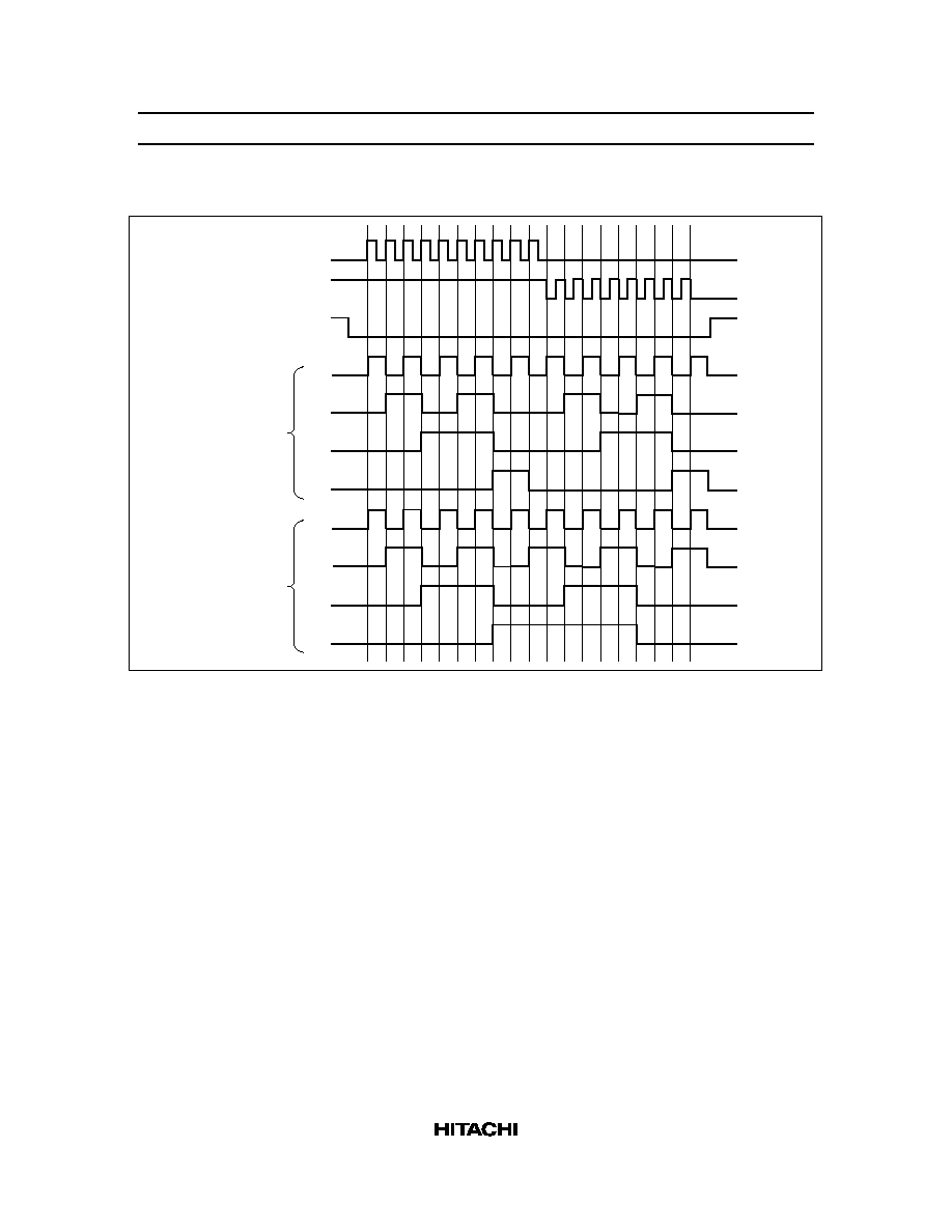
The HD74HC4518 dual BCD counter and the HD74HC4520 dual binary counter consist of two identical,
independent, internally synchronous 4-stage counters. The counter stages are type D flip-flops, with
interchangeable Clock and Enable lines for incrementing on either the positive-going or negative-going
transition as required when cascading multiple stages. Each counter can be cleared by applying a high
level on the Reset line. In addition, the HD74HC4518 will count out of all undefined states within two
clock periods. These complementary MOS up counters find primary use in multi-stage synchronous or
ripple counting applications requiring low power dissipation and/or high noise immunity.
Features
∑
High Speed Operation
∑
High Output Current: Fanout of 10 LSTTL Loads
∑
Wide Operating Voltage: V
CC
= 2 to 6 V
∑
Low Input Current: 1 ĶA max
∑
Low Quiescent Supply Current: I
CC
(static) = 4 ĶA max (Ta = 25įC)
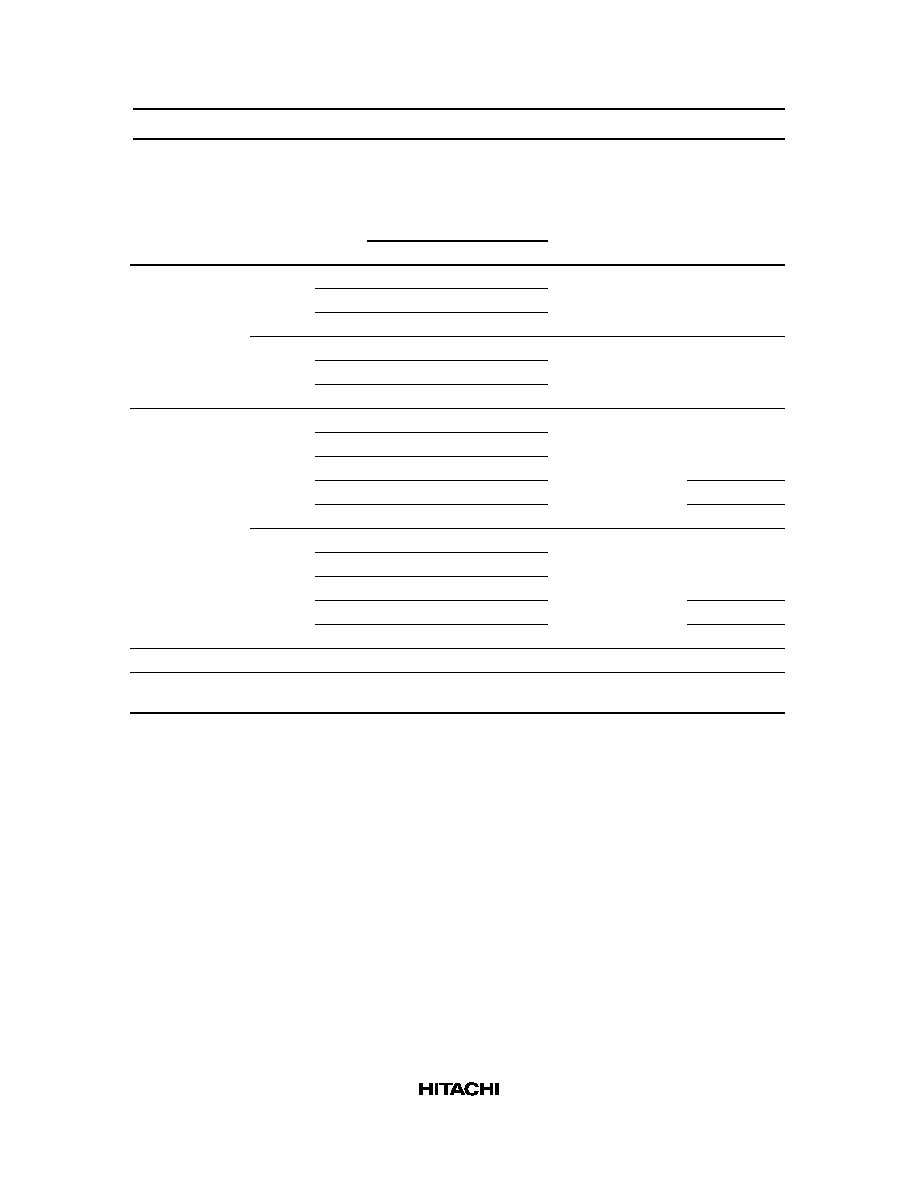
Function Table
Clock
Enable
Reset
Operation
H
L
Increment counter
L
L
Increment counter
X
L
No change
X
L
No change
L
L
No change
H
L
No change
X
X
H
Q
0
to Q
3
= L