HD74HC299
8-bit Universal Shift/Storage Register (with 3-state outputs)
Description
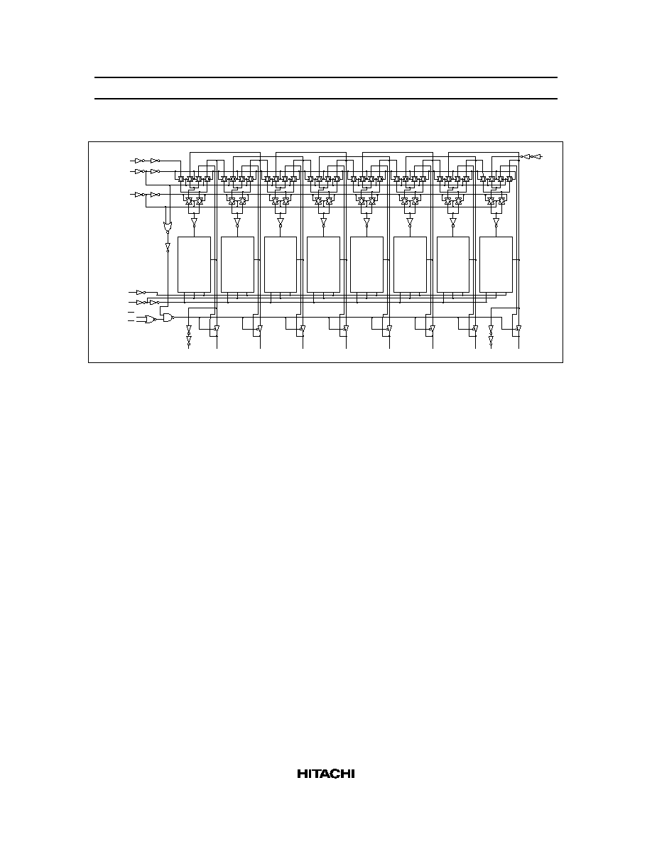
The HD74HC299 features multiplexed inputs/outputs to achieve full 8-bit data handling in a single 20-pin
package. Due to the large output drive capability and 3-state feature, this device is ideally suited for
interfacing with bus lines in a bus oriented system. Two function select inputs and two output control
inputs are used to choose the mode of operation as listed in the function table. Synchronous parallel
loading is accomplished by taking both function select lines S
0
and S
1
high. This places the 3-state outputs
in a high impedance state, which permits data applied to the input/output lines to be clocked into the
register. Reading out of the register can be done while the outputs are enabled in any mode. A direct
overriding clear input is provided to clear the register whether the outputs are enabled or disabled.
Features
∑
High Speed Operation
∑
High Output Current: Fanout of 15 LSTTL Loads
∑
Wide Operating Voltage: V
CC
= 2 to 6 V
∑
Low Input Current: 1 ĶA max
∑
Low Quiescent Supply Current: I
CC
(static) = 4 ĶA max (Ta = 25įC)

HD74HC299
2
Function Table
Inputs
Function
Select
Output
Control
Serial Inputs/Outputs
Outputs
Mode
Clear
S
1
S
0
G
1
G
2
Clock S
L
S
R
A/Q
A
B/Q
B
C/Q
C
D/Q
D
E/Q
E
F/Q
F
G/Q
G
H/Q
H
Q
A
'
Q
H
'
Clear
L
X
L
L
L
X
X
X
L
L
L
L
L
L
L
L
L
L
L
L
X
L
L
X
X
X
L
L
L
L
L
L
L
L
L
L
Hold
H
L
L
L
L
X
X
X
Q
A0
Q
B0
Q
C0
Q
D0
Q
E0
Q
F0
Q
G0
Q
H0
Q
A0
Q
H0
H
X
X
L
L
L
X
X
Q
A0
Q
B0
Q
C0
Q
D0
Q
E0
Q
F0
Q
G0
Q
H0
Q
A0
Q
H0
Shift
H
L
H
L
L
X
H
H
Q
An
Q
Bn
Q
Cn
Q
Dn
Q
En
Q
Fn
Q
Gn
H
Q
Gn
Right
H
L
H
L
L
X
L
L
Q
An
Q
Bn
Q
Cn
Q
Dn
Q
En
Q
Fn
Q
Gn
L
Q
Gn
Shift
H
H
L
L
L
H
X
Q
Bn
Q
Cn
Q
Dn
Q
En
Q
Fn
Q
Gn
Q
Hn
H
Q
Bn
H
Left
H
H
L
L
L
L
X
Q
Bn
Q
Cn
Q
Dn
Q
En
Q
Fn
Q
Gn
Q
Hn
L
Q
Bn
L
Load
H
H
H
X
X
X
X
a
b
c
d
e
f
g
h
a
h
Notes: 1. a to h; the level of steady-state input at inputs A through H, respectively. These data are
loaded into the flip-flop outputs are isolated from the input/output terminals.
2. Q
A0
to Q
H0
; the level of Q
A
through Q
H
, respectively, before the indicated steady-state input
conditions were established.
3. Q
An
to Q
Hn
; the level of Q
A
through Q
H
, respectively, before the most-recent
transition of the
clock.
4. = ; When one or both output controls are high the eight input/output terminals are desabled to
the high-impedance state, however, sequential operation or clearing of the register is not
affected.
5. When clear is low, outputs of Q
A
' and Q
H
' are low, in spite of other inputs.