HD74AC194
4-bit Bidirectional Unviersal Shift Register
Description
This bidirectional shift register is designed to incorporate virtually all of the features a system designer may
want in a shift register. It features parallel inputs, parallel outputs, right shift and left shift serial inputs,
operating mode control inputs, and a direct overriding clear line. The register has four destinct modes of
operation: parallel (broadside) load, shift right (in the direction Q
0
toward Q
3
); shift left; inhibit clock (do
nothing).
Synchronous parallel loading is accomplished by applying the four bits of data and taking both mode
control inputs, S
0
and S
1
, high. The data are loaded into their respective flip-flops and appear at the output
after the positive transition of the clock input. During loading, serial data flow is inhibited. Shift right is
accomplished synchronously with the rising edge of the clock pulse when S
0
is high and S
1
is low. Serial
date for this mode is entered at the shift right data input. When S
0
is low and S
1
is high, data shifts left
synchronously and new data is entered at the shifts left serial input. Clocking of the flip-flops is inhibited
when both mode control inputs are low. The mode control inputs should be changed only when the clock
input is high.
Features
·
Asynchronous Master Reset
·
Hole (Do Nothing) Mode
·
Outputs Source/Sink 24 mA
HD74AC194
2
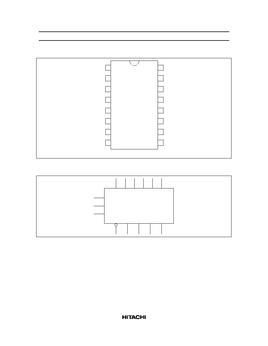
Pin Arrangement
1
2
3
4
5
6
7
8
16
15
14
13
12
11
10
9
MR
D
SR
P
0
P
1
P
2
D
SL
P
3
GND
V
CC
Q
0
Q
1
Q
2
Q
3
CP
S
1
S
0
(Top view)
Logic Symbol
S
0
D
SR
MR
Q
0
Q
1
Q
2
Q
3
D
SL
P
0
P
1
P
2
P
3
S
1
CP
Pin Names
S
0
, S
1
Mode Control Inputs
P
0
to P
3
Parallel Data Inputs
D
SR
Serial Data Input (Shift Right)
D
SL
Serial Data Input (Shift Left)
CP
Clock Pulse Input (Active Rising Edge)
MR
Asynchronous Master Reset Input (Active LOW)
Q
0
to Q
3
Parallel Outputs
HD74AC194
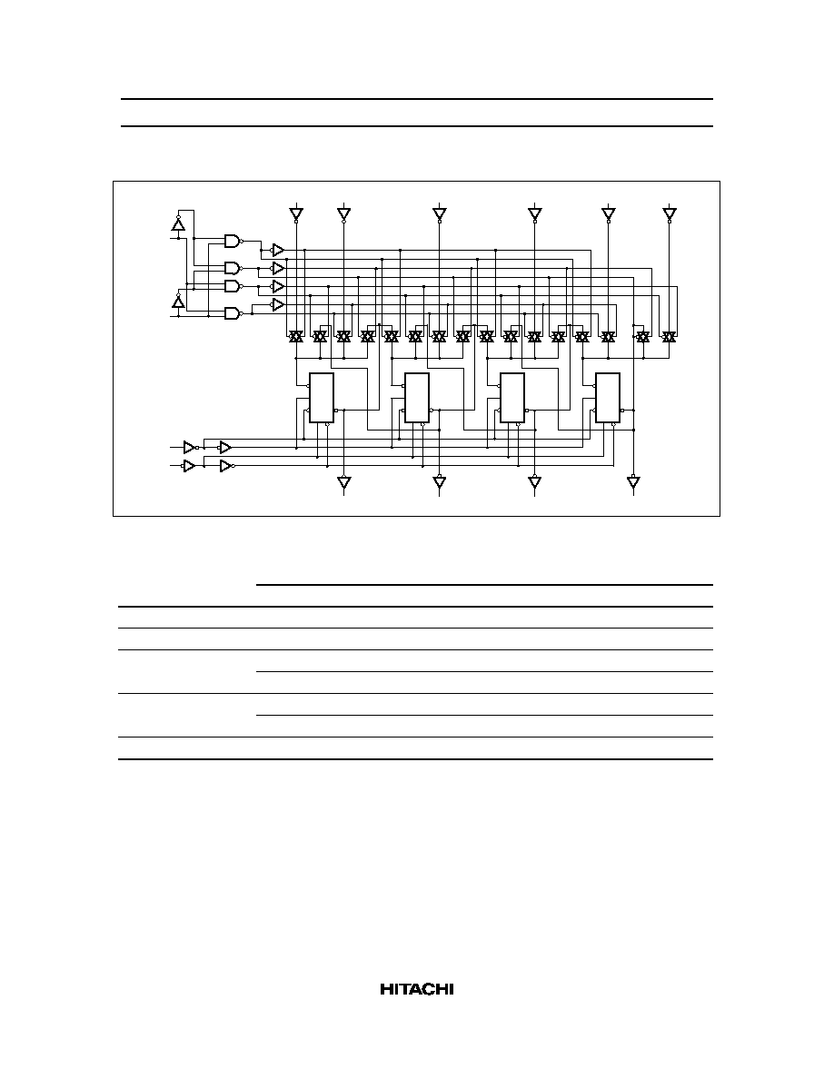
3
Logic Diagram
S
0
D
SL
P
3
P
2
P
1
P
0
D
SR
Q
0
Q
1
Q
2
Q
3
S
1
CP
MR
D
C
C
Q
CL CL
D
C
C
Q
CL CL
D
C
C
Q
CL CL
D
C
C
Q
CL CL
Mode Select Table
Inputs
Output
Operating Mode
MR
S
1
S
0
D
SR
D
SL
P
n
Q
0
Q
1
Q
2
Q
3
Reset
L
X
X
X
X
X
L
L
L
L
Hold
H
L
L
X
X
X
q
0
q
1
q
2
q
3
Shift Left
H
H
L
X
L
X
q
1
q
2
q
3
L
H
H
L
X
H
X
q
1
q
2
q
3
H
Shift Right
H
L
H
L
X
X
L
q
0
q
1
q
2
H
L
H
H
X
X
H
q
0
q
1
q
2
Parallel Load
H
H
H
X
X
p
n
p
0
p
1
p
2
p
3
H
: HIGH Voltage Level
L
: LOW Voltage Level
p
n
(q
n
) : Lower case letters indicate the state of the referenced input (or output) one setup time prior to the
LOW-to-HIGH clock transition
X
: Immaterial
HD74AC194
4
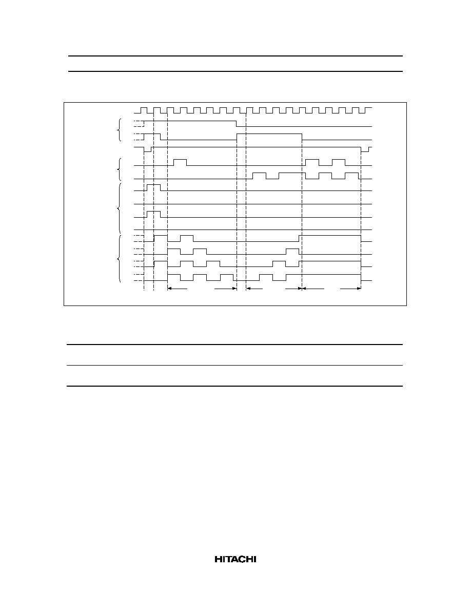
Timing Diagram
Mode
Control
Inputs
Parallel
Data
Inputs
Parallel
Data
Inputs
Outputs
CP
MR
S
0
S
1
P
0
P
1
P
2
P
3
Q
0
Q
1
Q
2
Q
3
D
SH
D
SL
Clear
Clear
Load
Shift Right
Shift Left
Inhibit
H
H
L
L
DC Characteristics (unless otherwise specified)
Item
Symbol
Max
Unit
Condition
Maximum quiescent supply current
I
CC
80
µ
A
V
IN
= V
CC
or ground, V
CC
= 5.5 V,
Ta = Worst case
Maximum quiescent supply current
I
CC
8.0
µ
A
V
IN
= V
CC
or ground, V
CC
= 5.5 V,
Ta = 25
°
C
HD74AC194
5
AC Characteristics: HD74AC194
Ta = +25
°
C
C
L
= 50 pF
Ta = 40
°
C to +85
°
C
C
L
= 50 pF
Item
Symbol
V
CC
(V)*
1
Min
Typ
Max
Min
Max
Unit
Maximum clock
f
max
3.3
7.5
--
65
MHz
frequency
5.0
100
--
85
Propagation delay
t
PLH
3.3
1.0
--
13.0
1.0
15.0
ns
CP to Q
n
5.0
1.0
--
10.0
1.0
11.5
Propagation delay
t
PHL
3.3
1.0
--
13.0
1.0
15.0
ns
CP to Q
n
5.0
1.0
--
10.0
1.0
11.5
Propagation delay
t
PHL
3.3
1.0
--
10.5
1.0
12.5
ns
MR
to Q
n
5.0
1.0
--
8.0
1.0
9.0
Note:
1. Voltage Range 3.3 is 3.3 V
±
0.3 V
Voltage Range 5.0 is 5.0 V
±
0.5 V
AC Operating Requirements: HD74AC194
Ta = +25
°
C
C
L
= 50 pF
Ta = 40
°
C
to +85
°
C
C
L
= 50 pF
Item
Symbol
V
CC
(V)*
1
Typ
Guaranteed Minimum
Unit
Setup time, HIGH or LOW
t
su
3.3
--
5.5
7.0
ns
Pn or D
SR
or D
SL
to CP
5.0
--
4.0
5.0
Hold time, HIGH or LOW
t
h
3.3
--
2.0
3.0
ns
Pn or D
SR
or D
SL
to CP
5.0
--
1.5
2.0
Setup time, HIGH or LOW
t
su
3.3
--
6.0
7.5
ns
S
n
to CP
5.0
--
4.5
5.5
Hold time, HIGH or LOW
t
h
3.3
--
0.0
0.0
ns
S
n
to CP
5.0
--
0.0
0.0
Recovery time
t
rec
3.3
--
0.5
0.5
ns
MR
to CP
5.0
--
0.5
0.5
Pulse width
t
w
3.3
--
5.5
7.0
ns
5.0
--
4.5
5.0
Note:
1. Voltage Range 3.3 is 3.3 V
±
0.3 V
Voltage Range 5.0 is 5.0 V
±
0.5 V