 | –≠–ª–µ–∫—Ç—Ä–æ–Ω–Ω—ã–π –∫–æ–º–ø–æ–Ω–µ–Ω—Ç: GS1540 | –°–∫–∞—á–∞—Ç—å:  PDF PDF  ZIP ZIP |

GENNUM CORPORATION P.O. Box 489, Stn. A, Burlington, Ontario, Canada L7R 3Y3
Tel. +1 (905) 632-2996 Fax. +1 (905) 632-5946 E-mail: info@gennum.com
www.gennum.com
Revision Date: August 2000
Document No. 522 - 27- 00
PRELIMINARY DATA SHEET
G
S
1
540
FEATURES
∑ SMPTE 292M compliant
∑ 1.485 and 1.485/1.001Gb/s operation
∑ integrated adjustment-free reclocker
∑ 1:20 serial to parallel conversion
∑ selectable reclocked serial output
∑ reclocker BYPASS capability
∑ LOCK detect
∑ input jitter indicator (IJI)
∑ 20 bit output
∑ 74.25MHz or 74.25/1.001MHz clock output
∑ single +5.0V power supply
∑ minimal component count for HD SDI receive
solutions
APPLICATIONS
SMPTE 292M Serial Digital Interfaces for Production
Switchers, Master Control Switchers, NLE's, and VTR's.
DESCRIPTION
The GS1540 is a high performance integrated Receiver
designed for HDTV component signals, conforming to the
SMPTE 292M standard. The GS1540 includes adjustment
free clock and data recovery, and 1:20 serial to parallel
conversion.
The Clock and Data Recovery stage was designed to
automatically recover the embedded clock signal and
retime the data from SMPTE 292M compliant digital video
signals. There is also a selectable reclocked serial data
buffer output and the ability to bypass the reclocker stage.
A unique feature, Input Jitter Indicator (IJI), is included for
robust system design. This feature is used to indicate
excessive input jitter before the chip mutes the outputs.
The Serial to Parallel conversion stage provides 1:20 S/P
conversion.
The GS1540 uses the GO1515 external VCO connected to
the internal PLL circuitry to achieve ultra low noise PLL
performance.
SIMPLIFIED BLOCK DIAGRAM
ORDERING INFORMATION
PART NUMBER
PACKAGE
TEMPERATURE
GS1540-CQR
128 pin MQFP
0∞C to 70∞C
RECLOCKER
CORE
S/P CONVERTER
BUFFER2
SDO_EN
SDO
SDO
DATA_OUT[19:0]
SDOint
SDOint
DDI
DDI_V
TT
(opt)
DDI
BUFFER1
PCLK_OUT
HD-LINX
TM
GS1540
HDTV Serial Digital
Non-Equalizing Receiver

GENNUM CORPORATION
522 - 27- 00
2
G
S
1
540
FUNCTIONAL BLOCK DIAGRAM
ABSOLUTE MAXIMUM RATINGS
T
A
= 25∞C, unless otherwise indicated.
PARAMETER
VALUE
Supply Voltage (V
S
)
5.5V
Input Voltage Range (any input)
V
EE
≠ 0.5 < V
IN
< V
CC
+ 0.5
Operating Temperature Range
0∞C
T
A
70∞C
Storage Temperature Range
-40∞C
T
S
150∞C
Power Dissipation (V
CC
= 5.25V)
1.85W
Lead Temperature (soldering 10 seconds)
260∞C
Input ESD Voltage
TBD
Junction Temperature
125∞C
PLL_LOCK
RECLOCKER CORE
S/P CONVERTER
CORE
BUFFER2
SDO_EN
BYPASS
SDO
SDO
DATA_OUT[19:0]
DDI
DDI_V
TT
(opt)
DDI
BUFFER1
PCLK_OUT
MUTE
PHASE
DETECTOR
CHARGE
PUMP
PHASE
LOCK
LOGIC
GO1515
BYP
ASS
MUX
LFS
PLCAP
IJI
PLCAP
LFS
VCO
LFA
LBCONT

GENNUM CORPORATION
522 - 27- 00
3
G
S
1
540
DC ELECTRICAL CHARACTERISTICS
V
CC
= 5V, V
EE
= 0V, T
A
= 0∞C to 70∞C, Data Rate = 1.485Gb/s.
PARAMETER
CONDITIONS
SYMBOL
MIN
TYP
MAX
UNITS
TEST LEVEL
Positive Supply Voltage
Operating range
V
CC
4.75
5.00
5.25
V
1
Power Consumption
V
CC
= 5; T
A
= 25∞c
P
D
-
1050
-
mW
5
Supply Current
V
CC
= 5; T
A
= 25∞C
I
S
-
210
-
mA 1
Output CM Voltage (SDO, SDO)
V
CM
3.75
4.0
4.25
V
5
Input DC Voltage (DDI, DDI)
-
4.0
-
V
1
Serial Inputs (DDI, DDI)
Differential mode
V
SID
100
-
1000
mV
7
Common mode
V
CM
2.5+V
SID/2
-
V
CC
-V
SID/2
V
7
High Level Input Voltage (BYPASS)
V
CC
= 5, T
A
= 25∞C
V
IH
2.0
-
-
V
1
Low Level Input Voltage (BYPASS)
V
CC
= 5, T
A
= 25∞C
V
IL
-
-
0.8
V
1
High Level Output Voltage
(D[19:0], PCLK)
V
CC
= 5, T
A
= 25∞C,
I
SOURCE
= 1.0mA
V
OH
2.4
-
3.0
V
1
Low Level Output Voltage
(D[19:0], PCLK)
V
CC
= 5, T
A
= 25∞C,
I
SINK
= 1.0mA
V
OL
-
-
0.4
V
1
High Level Output Voltage
(PLL_LOCK)
V
CC
= 5, T
A
= 25∞C,
I
SOURCE
= 200µA
V
OH
3.0
-
-
V
1
Low Level Output Voltage
(PLL_LOCK)
V
CC
= 5, T
A
= 25∞C,
I
SINK
= 500µA
V
OL
-
-
0.4
V
1
TEST LEVELS
1. Production test at room temperature and nominal supply voltage with guardbands for supply and temperature ranges.
2. Production test at room temperature and nominal supply voltage with guardbands for supply and temperature ranges using correlated
test.
3. Production test at room temperature and nominal supply voltage.
4. QA sample test.
5. Calculated result based on Level 1,2, or 3.
6. Not tested. Guaranteed by design simulations.
7. Not tested. Based on characterization of nominal parts.
8. Not tested. Based on existing design/characterization data of similar product.
AC ELECTRICAL CHARACTERISTICS - RECLOCKER STAGE
V
CC
= 5V, T
A
= 0∞C to 70∞C unless otherwise shown.
PARAMETER
CONDITIONS
SYMBOL
MIN
TYP
MAX
UNITS
TEST
LEVEL
Serial Input ≠
Data Rate
SMPTE 292M
BR
SDI
1.485/1.001
1.485
-
Gb/s
1
Serial Input ≠
Jitter Tolerance
Sinewave Modulation (p ≠ p)
J
TOL
-
0.5
-
UI
1
Phase Lock Time -
Asynchronous
Loop bandwidth approximately
1.4MHz @ 0.2 UI input jitter
modulation (LBCONT floating).
T
ALOCK
-
200
250
ms
7
Phase Lock Time -
Synchronous
Loop bandwidth approximately
1.4MHz @ 0.2 UI input jitter
modulation (LBCONT floating).
T
SLOCK
-
2
4
µs
7

GENNUM CORPORATION
522 - 27- 00
4
G
S
1
540
Carrier Detect Timer
Loop bandwidth approximately
1.4MHz @ 0.2 UI input jitter
modulation (LBCONT floating).
-
12
-
ms
7
Phase Lock/Unlock Timer
(1nF PLCAP)
Loop bandwidth approximately
1.4MHz @ 0.2 UI input jitter
modulation (LBCONT floating).
60
-
-
µs
7
Serial Output ≠ Signal Swing
V
SDO
320
400
480
mV
1
Serial Digital Output ≠
Rise and Fall Time
t
R-SDO
, t
F-SDO
-
150
270
ps
7
Serial Digital Output ≠
Rise and Fall Time Mismatch
-
-
100
ps
7
Serial Digital Output ≠
Intrinsic Jitter
(RMS Jitter for clean PRN 2
23
≠ 1
input on DDI/DDI inputs)
t
IJ
-
10
-
ps
2
Loop bandwidth
@ 0.2UI jitter modulation
LBCONT floating
-
1.4
-
MHz
7
Jitter peaking
-
-
0.1
dB
7
AC ELECTRICAL CHARACTERISTICS - SERIAL TO PARALLEL STAGE
V
CC
= 5V, T
A
= 0∞C to 70∞C unless otherwise shown.
PARAMETER
CONDITIONS
SYMBOL
MIN
TYP
MAX
UNITS
TEST LEVEL
Parallel Output Clock Frequency
SMPTE 292M
P
CLK_OUT
74.25/1.001
74.25
-
MHz
1
Clock Pulse Width Low
15pF load
t
PWL
5
7
-
ns
7
Clock Pulse Width High
15pF load
t
PWH
5
6
-
ns
7
Output signal Rise/Fall time
15pF load
t
r
, t
f
-
2000
4000
ps
7
Output Signal Rise/Fall Time Matching
15pF load
t
rfm
-
1000
2000
ps
7
Output Setup Time
15pF load
t
OD
4
6
-
ns
2
Output Hold Time
15pF load
t
OH
5
7
-
ns
2
TEST LEVELS
1. Production test at room temperature and nominal supply voltage with guardbands for supply and temperature ranges.
2. Production test at room temperature and nominal supply voltage with guardbands for supply and temperature ranges using
correlated test.
3. Production test at room temperature and nominal supply voltage.
4. QA sample test.
5. Calculated result based on Level 1,2, or 3.
6. Not tested. Guaranteed by design simulations.
7. Not tested. Based on characterization of nominal parts.
8. Not tested. Based on existing design/characterization data of similar product.
AC ELECTRICAL CHARACTERISTICS - RECLOCKER STAGE (Continued)
V
CC
= 5V, T
A
= 0∞C to 70∞C unless otherwise shown.
PARAMETER
CONDITIONS
SYMBOL
MIN
TYP
MAX
UNITS
TEST
LEVEL
GE
NN
U
M
C
O
RP
ORA
T
I
O
N
52
2 -
27-
00
5
GS
1540
P
I
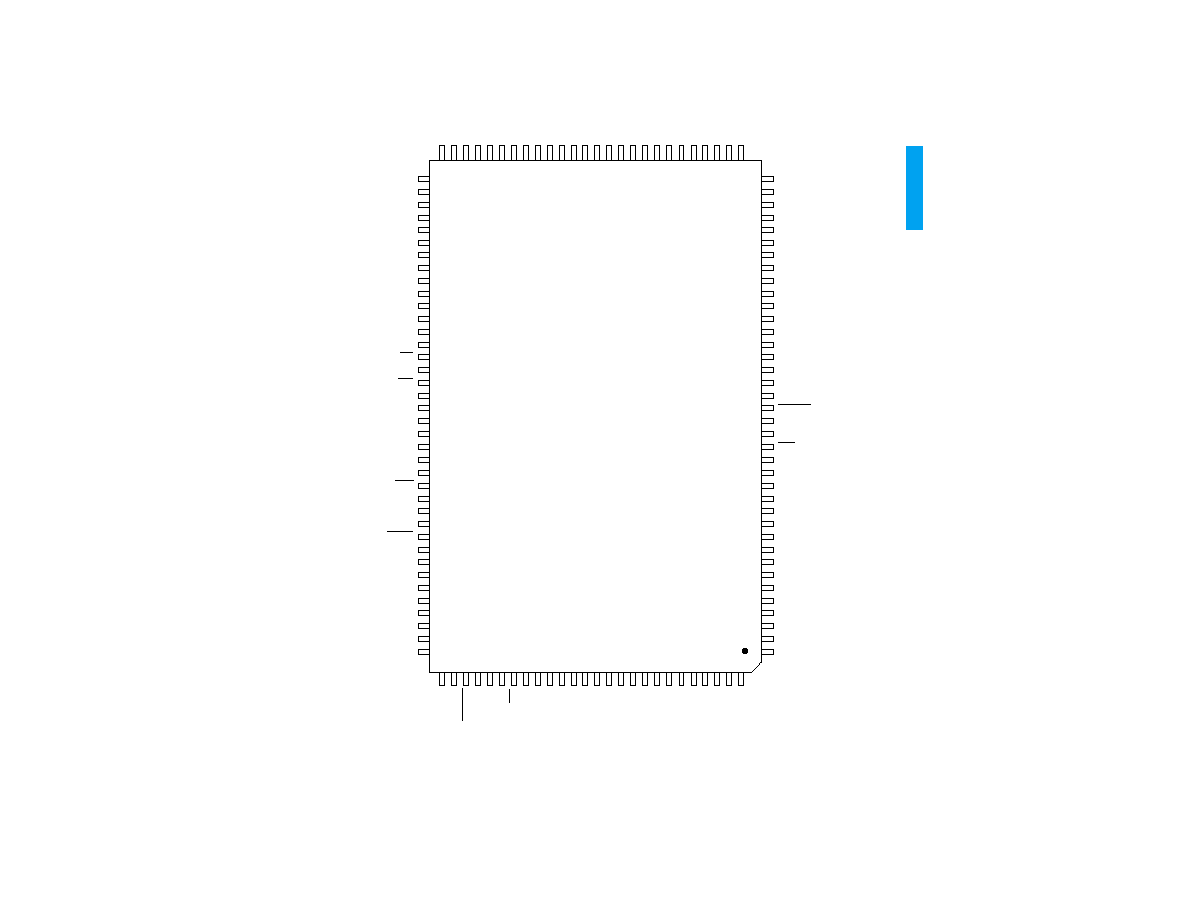
N CO
NNE
CTIO
NS
NC
NC
PCLK_V
EE
PCLK_V
CC
PCLK_OUT
SP_V
EE
SP_V
EE
SP_V
CC
SP_V
CC
NC
NC
NC
NC
NC
NC
NC
NC
SDO_V
CC
SDO_EN
SDO_V
EE
SDO
SDO
NC
NC
NC
NC
NC
NC
NC
NC
NC
NC
NC
NC
NC
NC
NC
NC
NC
NC
NC
NC
NC
NC
LF
A_V
CC
LF
A
LBCONT
LF
A_V
EE
DFT_V
EE
NC
NC
DM
DM
LFS
NC
NC
NC
LFS
IJI
NC
NC
VCO
NC
VCO
NC
PLCAP
NC
NC
PLCAP
NC
PLL_LOCK
NC
NC
NC
NC
DATA_OUT[19]
DATA_OUT[18]
DATA_OUT[17]
DATA_OUT[16]
DATA_OUT[15]
DATA_OUT[14]
NC
NC
DATA_OUT[13]
DATA_OUT[12]
DATA_OUT[11]
DATA_OUT[10]
NC
NC
DATA_OUT[9]
DATA_OUT[8]
DATA_OUT[7]
DATA_OUT[6]
DATA_OUT[5]
DATA_OUT[4]
DATA_OUT[3]
DATA_OUT[2]
DATA_OUT[1]
DATA_OUT[0]
NC
NC
NC
NC
BYPASS
DDI_V
TT
NC
DDI
DDI
PD_V
CC
NC
PDSUB_V
EE
PD_V
EE
NC
NC
NC
NC
NC
NC
NC
NC
NC
NC
NC
NC
NC
NC
NC
38
37
36
35
34
33
32
31
30
29
28
27
26
25
24
23
22
21
20
19
18
17
16
15
14
13
12
11
10
9
8
7
6
5
4
3
2
1
65
66
67
68
69
70
71
72
73
74
75
76
77
78
79
80
81
82
83
84
85
86
87
88
89
90
91
92
93
94
95
96
97
98
99
100
101
102
64
63
62
61
60
59
58
57
56
55
54
53
52
51
50
49
48
47
46
45
44
43
42
41
40
39
103
104
105
106
107
108
109
110
111
112
113
114
115
116
117
118
119
120
121
122
123
124
125
126
127
128
GS1540
TO
P
VIEW
NC