
DS04-13514-2E
FUJITSU SEMICONDUCTOR
DATA SHEET
Linear IC Converter
CMOS
D/A Converter for Digital Tuning
MB40D001
s
DESCRIPTION
The MB40D001 is an 8-bit D/A converter with 12 built-in channels. The 12 sets of analog outputs have built-in
OP amps to enable use with large current drive applications.
CS (chip select) data input/output format is used to enable connection to a serial bus. A built-in 12-bit I/O expander
provides serial <=> parallel conversion (8 of the 12 bits are also used with analog output).
The MB40D001 can be adapted for microcontroller port expansion, or replacement of electronic volume control
or semi-fixed calibration resistance.
Also, the MB40D001 is function- and pin-compatible with the MB88146A, for easy replacement when reducing
sysytem operating voltage.
s
FEATURES
∑ Supply voltage 2.7 V to 3.6 V (Power consumption 0.7 mW/ch typ.)
∑ Compact package: SSOP-24
∑ R-2R type 8-bit D/A converter with 12 built-in channels
∑ Built-in 12-bit I/O expander (8 of 12 bits also used with analog output)
∑ Built-in analog amplifier (sink current max. 0.4 mA, source current max. 1.0 mA)
∑ Built-in power-on detector circuit (detects VccD power-on, and performs initialization)
∑ Separate MCU interface power supply (VccD), OP amp supply (VccA), D/A converter supply V
DD
∑ Analog output range 0 V to VccA.
∑ Serial data input/output operation to maximum of 2.5 MHz (1.5 MHz in cascade operation)
∑ CMOS process
s
PACKAGES
24-pin plastic SSOP
(FPT-24P-M03)
3
MB40D001
s
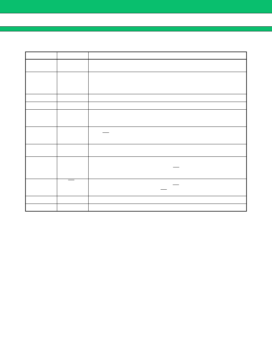
PIN DESCRIPTION
*1: Be sure that V
CC
A
V
CC
D, and that V
CC
A
V
DD
.
*2: Do not leave this pin in floating state.
Pin no.
Symbol
Description
1 to 4
AO
1
to AO
4
D/A converter analog output pins (V
DD
-GND output).
(Default state: #00 setting level output)
5 to 12
D
11
/AO
5
to
D
4
/AO
12
I/O expander parallel I/O pins (VccA/GND output 0.5 VccA/0.2 VccA input), also
used as D/A converter analog output pins (V
DD
- GND output).
Pin state is controlled by input data.
See "Data Configuration". (Default state: Input mode, high-impedance state.)
13
V
DD
*
1
D/A converter reference power supply pin.
14
V
CC
D*
1
MCU interface power supply (Power supply for I/O expander).
15 to 18
D
3
to D
0
I/O expander parallel I/O pins (VccD/GND output 0.5 VccD/0.2VccD input).
Pin state is controlled by input data.
See "Data Configuration". (Default state: Input mode, high-impedance state.)
19
CLK*
2
Shift clock input pin.
When CS = "L", SI data is loaded into the shift register at the rise of the shift
clock signal.
20
SI*
2
Data input pin (serial input pin).
Used for 16-bit serial data input.
21
SO
Data output pin (serial output pin).
First-bit (LSB) data from the 16-bit shift register is output in synchronization
with the fall of the shift clock signal. When CS = "H", this pin is in high
impedance state.
22
CS*
2
Chip select signal input pin.
Input to shift registers is enabled when the CS signal falling edges. Shift register
contents can be executed when the CS signal rising edges.
23
V
CC
A*
1
Analog unit power supply pin (Power supply for the OP amp.).
24
GND
Common GND pin.


