 | ÐлекÑÑоннÑй компоненÑ: SSTV16859 | СкаÑаÑÑ:  PDF PDF  ZIP ZIP |
Äîêóìåíòàöèÿ è îïèñàíèÿ www.docs.chipfind.ru
© 2002 Fairchild Semiconductor Corporation
DS500414
www.fairchildsemi.com
March 2001
Revised July 2002
SSTV168
59 Dual
Out
put
13-
Bit
Regi
ster
wi
th
SSTL-2
Compati
b
le
I
/
O a
nd Reset
SSTV16859
Dual Output 13-Bit Register with
SSTL-2 Compatible I/O and Reset
General Description
The SSTV16859 is a dual output 13-bit register designed
for use with 184 and 232 pin DDR-1 memory modules. The
device has a differential input clock, SSTL-2 compatible
data inputs and a LVCMOS compatible RESET input. The
device has been designed to meet the JEDEC DDR mod-
ule register specifications.
The device has been fabricated on an advanced sub-
micron CMOS process and is designed to operate at power
supplies of less than 3.6V's.
Features
I
Compliant with DDR-I registered module specifications
I
Operates at 2.5V
±
0.2V V
DD
I
SSTL-2 compatible input structure
I
SSTL-2 compliant output structure
I
Differential SSTL-2 compatible clock inputs
I
Low power mode when device is reset
I
Industry standard 64 pin TSSOP package
I
Also packaged in plastic Fine-Pitch Ball Grid Array
(FBGA)
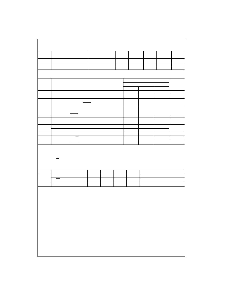
Ordering Code:
Note 1: Ordering code "G" indicates Trays.
Note 2: Devices also available in Tape and Reel. Specify by appending the suffix letter "X" to the ordering code.
Order Number
Package Number
Package Description
SSTV16859G
(Note 1)(Note 2)
BGA96A
96-Ball Fine-Pitch Ball Grid Array (FBGA), JEDEC MO-205, 5.5mm Wide
SSTV16859MTD
(Note 2)
MTD64
64-Lead Thin Shrink Small Outline Package (TSSOP), JEDEC MO-153, 6.1mm Wide
www.fairchildsemi.com
2
SSTV16859
Connection Diagrams
Pin Assignment for TSSOP
Pin Assignment for FBGA
(Top Thru View)
Pin Descriptions
FBGA Pin Assignments
Truth Table
L
=
Logic LOW
H
=
Logic HIGH
X
=
Don't Care but not floating unless noted
=
LOW-to-HIGH Clock Transition
=
HIGH-to-LOW Clock Transition
Q
n-1
= Output Remains in Previously Clocked State
Pin Name
Description
Q
1A
-Q
13A
SSTL-2 Compatible Register Outputs
Q
1B
-Q
13B
D
1
-D
13
SSTL-2 Compatible Register Inputs
RESET
Asynchronous LVCMOS Reset Input
CK
Positive Master Clock Input
CK
Negative Master Clock Input
V
REF
Voltage Reference Pin for SSTL level inputs
V
DDQ
Power Supply Voltage for Output Signals
V
DD
Power Supply Voltage for Inputs
NC
Electrically Isolated No Connect
1
2
3
4
5
6
A
NC
NC
NC
NC
NC
NC
B
Q
12A
Q
13A
GND
GND
NC
NC
C
Q
10A
Q
11A
GND
GND
NC
NC
D
Q
8A
Q
9A
V
DDQ
V
DDQ
D
13
D
12
E
Q
6A
Q
7A
V
DDQ
V
DD
D
11
D
10
F
Q
4A
Q
5A
V
DDQ
V
DD
D
9
D
8
G
Q
2A
Q
3A
GND
GND
D
7
RESET
H
Q
1A
Q
13B
GND
GND
NC
CK
J
Q
12B
Q
11B
GND
V
REF
NC
CK
K
Q
10B
Q
9B
V
DDQ
V
DD
NC
NC
L
Q
8B
Q
7B
V
DDQ
V
DD
D
5
D
6
M
Q
6B
Q
5B
V
DDQ
V
DDQ
D
3
D
4
N
Q
4B
Q
3B
GND
GND
D
1
D
2
P
Q
2B
Q
1B
GND
GND
NC
NC
R
NC
NC
NC
NC
NC
NC
T
NC
NC
NC
NC
NC
NC
RESET
D
n
CK
CK
Q
n
L
X or
Floating
X or
Floating
X or
Floating
L
H
L
L
H
H
H
H
X
L
H
Q
n-1
H
X
H
L
Q
n-1
3
www.fairchildsemi.com
SSTV168
59
Functional Description
The SSTV16859 is a 13-bit dual register with SSTL-2 com-
patible inputs and outputs. Input data is transferred to out-
put data on the rising edge of the differential clock pair.
When the RESET signal is asserted LOW all outputs are
placed into the LOW logic state and all input comparators
are disabled for power savings. Output glitches are pre-
vented by disabling the internal registers more quickly than
the input comparators. When RESET is removed, the sys-
tem designer must insure the clock and data inputs to the
device are stable during the rising transition of the RESET
signal.
The SSTL-2 data inputs transition based on the value of
V
REF
. V
REF
is a stable system reference used for setting
the trip point of the input buffers of the SSTV16859 and
other SSTL-2 compatible devices.
The RESET signal is a standard CMOS compatible input
and is not referenced to the V
REF
signal.
Logic Diagram
For n
=
1 to 13
www.fairchildsemi.com
4
SSTV16859
Absolute Maximum Ratings
(Note 3)
Recommended Operating
Conditions
(Note 5)
Note 3: The "Absolute Maximum Ratings" are those values beyond which
the safety of the device cannot be guaranteed. The device should not be
operated at these limits. The parametric values defined in the "Electrical
Characteristics" table are not guaranteed at the absolute maximum ratings.
The "Recommended Operating Conditions" table will define the conditions
for actual device operation.
Note 4: IO Absolute Maximum Rating must be observed.
Note 5: The RESET input of the device must be held at V
DD
or GND to
ensure proper device operation. The differential inputs must not be floating,
unless RESET is asserted LOW.
DC Electrical Characteristics
(2.3V
V
DD
2.7V)
Supply Voltage (V
DDQ
)
-
0.5V to
+
3.6V
Supply Voltage (V
DD
)
-
0.5V to
+
3.6V
Reference Voltage (V
REF
)
-
0.5V to
+
3.6V
Input Voltage (V
I
)
-
0.5V to V
DD
+
0.5V
Output Voltage (V
O
)
Outputs Active (Note 4)
-
0.5V to V
DDQ
+
0.5V
DC Input Diode Current (I
IK
)
V
I
<
0V
-
50 mA
V
I
>
V
DD
+
50 mA
DC Output Diode Current (I
OK
)
V
O
<
0V
-
50 mA
V
O
>
V
DDQ
+
50 mA
DC Output Source/Sink Current
(I
OH
/I
OL
)
±
50 mA
DC V
DD
or Ground Current
per Supply Pin (I
DD
or Ground)
±
100 mA
Storage Temperature Range (T
stg
)
-
65
°
C to
+
150
°
C
ESD (Human Body Model)
7000V
Power Supply (V
DDQ
)
2.3V to 2.7V
Power Supply (V
DD
)
Operating Range
V
DDQ
to 2.7V
Reference Supply
(V
REF
=
V
DDQ
/2)
1.15 to 1.35
Termination Voltage (V
TT
)
V
REF
±
40 mV
Input Voltage
0 to V
DD
Output Voltage (V
O
)
Output in Active States
0V to V
DDQ
Output Current I
OH
/I
OL
V
DD
=
2.3V to 2.7V
±
20 mA
Free Air Operating Temperature (T
A
)
0
°
C to
+
70
°
C
Symbol
Parameter
Conditions
V
DD
Min
Typ
Max
Units
(V)
V
IKL
Input LOW Clamp Voltage
I
I
=
-
18 mA
2.3
-
1.2
V
V
IKH
Input HIGH Clamp Voltage
I
I
=
+
18 mA
2.3
3.5
V
V
IH-AC
AC HIGH Level Input Voltage
Data Inputs
V
REF
+
310mV
V
V
IL-AC
AC LOW Level Input Voltage
Data Inputs
V
REF
-
310mV
V
V
IH-DC
DC HIGH Level Input Voltage
Data Inputs
V
REF
+
150mV
V
V
IL-DC
DC LOW Level Input Voltage
Data Inputs
V
REF
-
150mV
V
V
IH
HIGH Level Input Voltage
RESET
1.7
V
V
IL
LOW Level Input Voltage
RESET
0.7
V
V
ICR
Common Mode Input Voltage Range CK, CK
0.97
1.53
V
V
I(PP)
Peak to Peak Input Voltage
CK, CK
360
mV
V
OH
HIGH Level Output Voltage
I
OH
=
-
100
µ
A
2.3 to 2.7
V
DD
-
0.2
V
I
OH
=
-
16 mA
2.3
1.95
V
OL
LOW Level Output Voltage
I
OL
=
100
µ
A
2.3 to 2.7
0.2
V
I
OL
=
16 mA
2.3
0.35
I
I
Input Leakage Current
V
I
=
V
DD
or GND
2.7
±
5.0
µ
A
I
DD
Static Standby
RESET
=
GND, I
O
=
0
2.7
10
µ
A
Static Operating
RESET
=
V
DD
, I
O
=
0
25
mA
V
I
=
V
IH(AC)
or V
IL(AC)
I
DDD
Dynamic Operating Current
RESET
=
V
DD
, I
O
=
0
2.7
µ
A/MHz
Clock Only
V
I
=
V
IH(AC)
or V
IL(AC)
120
CK, CK Duty Cycle 50%
Dynamic Operating Current
RESET
=
V
DD
, I
O
=
0
µ
A/MHz
per Data Input
V
I
=
V
IH(AC)
or V
IL(AC)
CK, CK Duty Cycle 50%
15
Data Input
=
½ Clock
Rate 50% Duty Cycle
5
www.fairchildsemi.com
SSTV168
59
DC Electrical Characteristics
(Continued)
AC Electrical Characteristics
(Note 6)
Note 6: Refer to Figure 1 through Figure 7.
Note 7: This parameter is not production tested.
Note 8: For data signal input slew rate
1 V/ns.
Note 9: For data signal input slew rate
0.5 V/ns and
<
1 V/ns.
Note 10: For CK, CK signals input slew rates are
1 V/ns.
Capacitance
(Note 11)
Note 11: T
A
=
+
25
°
C, f
=
1 MHz, Capacitance is characterized but not tested.
Symbol
Parameter
Conditions
V
DD
Min
Typ
Max
Units
(V)
R
OH
Output HIGH On Resistance
I
OH
=
-
20 mA
2.3 to 2.7
7
20
R
OL
Output LOW On Resistance
I
OL
=
20 mA
2.3 to 2.7
7
20
R
O
| R
OH
- R
OL
|
I
O
=
20 mA, T
A
=
25
°
C
2.5
4
Symbol
Parameter
T
A
=
0
°
C to
+
70
°
C, C
L
=
30 pF, R
L
=
50
Units
V
DD
=
2.5V
±
0.2V; V
DDQ
=
2.5V
±
0.2V
Min
Typ
Max
f
MAX
Maximum Clock Frequency
200
MHz
t
W
Pulse Duration, CK, CK HIGH or LOW (Figure 2)
2.5
ns
t
ACT
Differential Inputs Activation Time,
22
ns
(Note 7)
data inputs must be LOW after RESET HIGH (Figure 3)
t
INACT
Differential Inputs De-activation Time,
22
ns
(Note 7)
data and clock inputs must be held at valid levels
(not floating) after RESET LOW
t
S
Setup Time, Fast Slew Rate (Note 8)(Note 9) (Figure 5)
0.75
ns
Setup Time, Slow Slew Rate (Note 9)(Note 10) (Figure 5)
0.9
t
H
Hold Time, Fast Slew Rate (Note 8)(Note 10) (Figure 5)
0.75
ns
Hold Time, Slow Slew Rate (Note 9)(Note 10) (Figure 5)
0.9
t
REM
Reset Removal Time (Figure 7)
10
ns
t
PHL
, t
PLH
Propagation Delay CK, CK to Q
n
(Figure 4)
1.1
2.8
ns
t
PHL
Propagation Delay RESET to Q
n
(Figure 6)
5.0
ns
Symbol
Parameter
Min
Typ
Max
Units
Conditions
C
IN
Data Pin Input Capacitance
2.2
3.2
pF
V
DD
=
2.5V, V
I
=
V
REF
±
310 mV
CK, CK - Input Capacitance
2.2
3.2
pF
V
DD
=
2.5V, V
ICR
=
1.25, V
I(PP)
=
360 mV
RESET
2.3
3.3
pF
V
DD
=
2.5V, V
I
=
V
DD
or GND