 | ÐлекÑÑоннÑй компоненÑ: SMCJ8V0C | СкаÑаÑÑ:  PDF PDF  ZIP ZIP |
Äîêóìåíòàöèÿ è îïèñàíèÿ www.docs.chipfind.ru
SMCJ5V0(C)A - SMCJ170(C)A
SMCJ5V0(C)A-SMCJ170(C)A, Rev. H1
Transient Voltage Suppressors
SMCJ5V0(C)A - SMCJ170(C)A
1500 Watt Transient Voltage Suppressors
Absolute Maximum Ratings*
T
A
= 25°C unless otherwise noted
2003 Fairchild Semiconductor Corporation
Symbol
Parameter
Value
Units
P
PPM
Peak Pulse Power Dissipation on 10/1000
µ
s waveform
1500 W
I
PPM
Peak Pulse Current on 10/1000
µ
s waveform
see table
A
I
FSM
Non-repetitive Peak Forward Surge Current
superimposed on rated load (JEDEC method)
(Note 1)
200 A
T
stg
Storage Temperature Range
-55 to +150
°
C
T
J
Operating Junction Temperature
+ 150
°
C
Features
·
Glass passivated junction.
·
1500 W Peak Pulse Power capability
on 10/1000
µ
s waveform.
·
Excellent clamping capability.
·
Low incremental surge resistance.
·
Fast response time; typically less
than 1.0 ps from 0 volts to BV for
unidirectional and 5.0 ns for
bidirectional.
·
Typical I
R
less than 1.0
µ
A above 10V.
·
UL certified, UL #E210467.
DEVICES FOR BIPOLAR APPLICATIONS
- Bidirectional types use CA suffix.
- Electrical Characteristics apply in both directions.
*
These ratings are limiting values above which the serviceability of any semiconductor device may be impaired.
Note 1: Measured on 8.3 ms single half-sine wave or equivalent square wave; Duty cycle = 4 pulses per minute maximum.
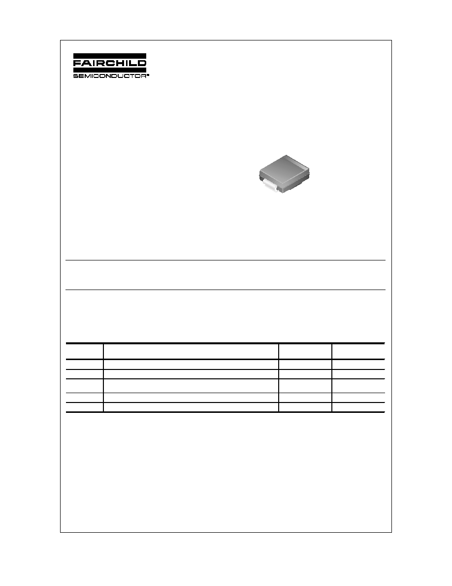
SMC/DO-214AB
COLOR BAND DENOTES CATHODE
ON UNIDIRECTIONAL DEVICES ONLY.
NO COLOR BAND ON BIDIRECTIONAL
DEVICES.
SMCJ5V0(C)A - SMCJ170(C)A
SMCJ5V0(C)A-SMCJ170(C)A, Rev. H1
Transient Voltage Suppressors
(continued)
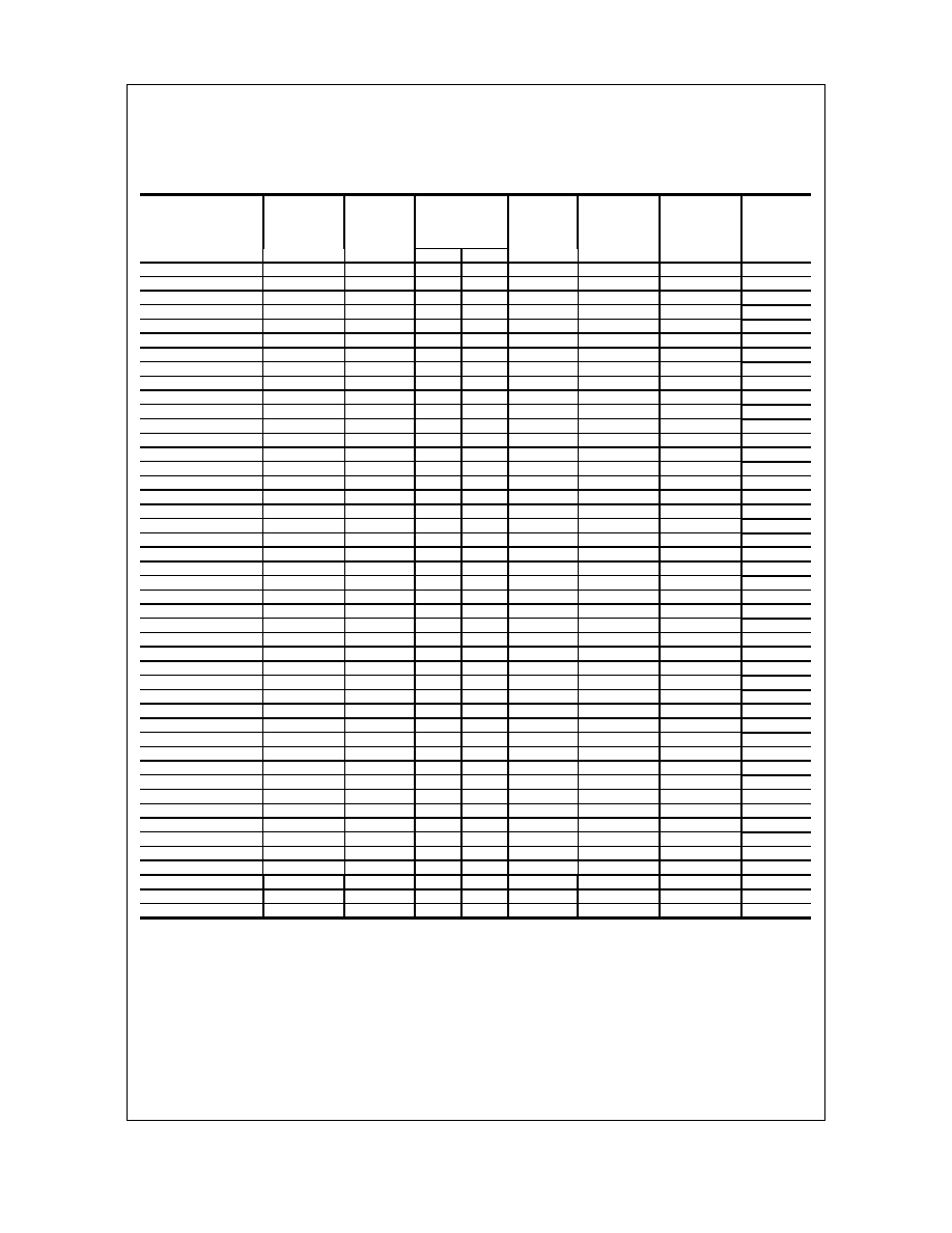
Electrical Characteristics
T
A
= 25°C unless otherwise noted
* Color band denotes cathode on unidirectional devices only. No color band on bidirectional devices.
** For bidirectional parts with V
RWM
<10V, the I
R
max limit is doubled.
U ni-directional
B i-directional (C )
D evice
Part
M arking*
R everse
Stand-off
Voltage
V
R W M
(V)
B reakdow n
Voltage
V
B R
(V)
Test
C urrent
I
T
(m A)
C lam ping
Voltage
@ I
PPM
V
C
(V)
Peak Pulse
C urrent
I
PPM
(A )
R everse
Leakage
@ V
R W M
I
R
(uA )**
m in
m ax
SM C J5V0(C )A
GD E
5.0
6.40
7.0
10
9.2
163.0
1000
SM C J6V0(C )A
GD G
6.0
6.67 7.37
10
10.3
145.6
1000
SM C J6V5(C )A
GD K
6.5
7.22 7.98
10
11.2
133.9
500
SM C J7V0(C )A
GD M
7.0
7.78 8.60
10
12.0
125.0
200
SM C J7V5(C )A
GD P
7.5
8.33 9.21
1
12.9
116.3
100
SM C J8V0(C )A
GD R
8.0
8.89 9.83
1
13.6
110.3
50
SM C J8V5(C )A
GD T
8.5
9.44 10.4
1
14.4
104.2
20
SM C J9V0(C )A
GD V
9.0
10.0 11.1
1
15.4
97.4
10
SM C J10(C)A
GD X
10
11.1 12.3
1
17.0
88.2
5
SM C J11(C)A
GD Z
11
12.2 13.5
1
18.2
82.4
5
SM C J12(C)A
GE E
12
13.3 14.7
1
19.9
75.3
5
SM C J13(C)A
GE G
13
14.4 15.9
1
21.5
69.8
5
SM C J14(C)A
GE K
14
15.6 17.2
1
23.2
64.7
5
SM C J15(C)A GE M
15
16.7
18.5
1 24.4
61.5 5
SM C J16(C)A GE P
16
17.8
19.7
1 26.0
57.7 5
SM C J17(C)A GE R
17
18.9
20.9
1 27.6
54.3 5
SM C J18(C)A GE T
18
20.0
22.1
1 29.2
51.4
5
SM C J20(C)A GE V
20
22.2
24.5
1 32.4
46.3 5
SM C J22(C)A GE X
22
24.4
26.9
1 35.5
42.3 5
SM C J24(C)A GE Z
24
26.7
29.5
1 38.9
38.6
5
SM C J26(C)A GFE
26
28.9
31.9
1 42.1
35.6
5
SM C J28(C)A GFG
28
31.1
34.4
1 45.4
33.0 5
SM C J30(C)A GFK
30
33.3
36.8
1 48.4
31.0
5
SM C J33(C)A GFM
33
36.7
40.6
1 53.3
28.1 5
SM C J36(C)A GFP
36
40.0
44.2
1 58.1
25.8
5
SM C J40(C)A GFR
40
44.4
49.1
1 64.5
23.3 5
SM C J43(C)A GFT
43
47.8
52.8
1
69.4
21.6
5
SM C J45(C)A GFV
45
50.0
55.3
1 72.7
20.6
5
SM C J48(C)A GFX
48
53.3
58.9
1 77.4
19.4
5
SM C J51(C)A GFZ
51
56.7
62.7
1
82.4
18.2
5
SM C J54(C)A GG E
54
60.0
66.3
1 87.1
17.2 5
SM C J58(C)A GG G
58
64.4
71.2
1 93.6
16.0 5
SM C J60(C)A GG K
60
66.7
73.7
1 96.8
15.5 5
SM C J64(C )A GG M
64
71.1
78.6
1
103.0
14.6 5
SM C J70(C)A GG P
70
77.8
86.0
1
113.0
13.3 5
SM C J75(C)A GG R
75
83.3
92.1
1
121.0
12.4 5
SM C J78(C)A GG T
78
86.7
95.8
1
126.0
11.9 5
SM C J85(C)A GG V
85
94.4
104.0
1
137.0
10.9 5
SM C J90(C)A GG X
90
100.0
111.0
1
146.0
10.3 5
SM C J100(C)A GG Z
100
111.0
123.0
1 162.0 9.3 5
SM C J110(C)A GH E
110
122.0
135.0
1 177.0 8.5 5
SM C J120(C)A GH G
120
133.0
147.0
1 193.0 7.8 5
SM C J130(C)A GH K
130
144.0
159.0
1 209.0 7.2 5
SM C J150(C)A GH M
150
167.0
185.0
1 243.0 6.2 5
SM C J160(C )A GH P
160
178.0
197.0
1 259.0 5.8 5
SM C J170(C)A GH R
170
189.0
209.0
1 275.0 5.5 5
SMCJ5V0(C)A - SMCJ170(C)A
SMCJ5V0(C)A-SMCJ170(C)A, Rev. H1
Transient Voltage Suppressors
(continued)
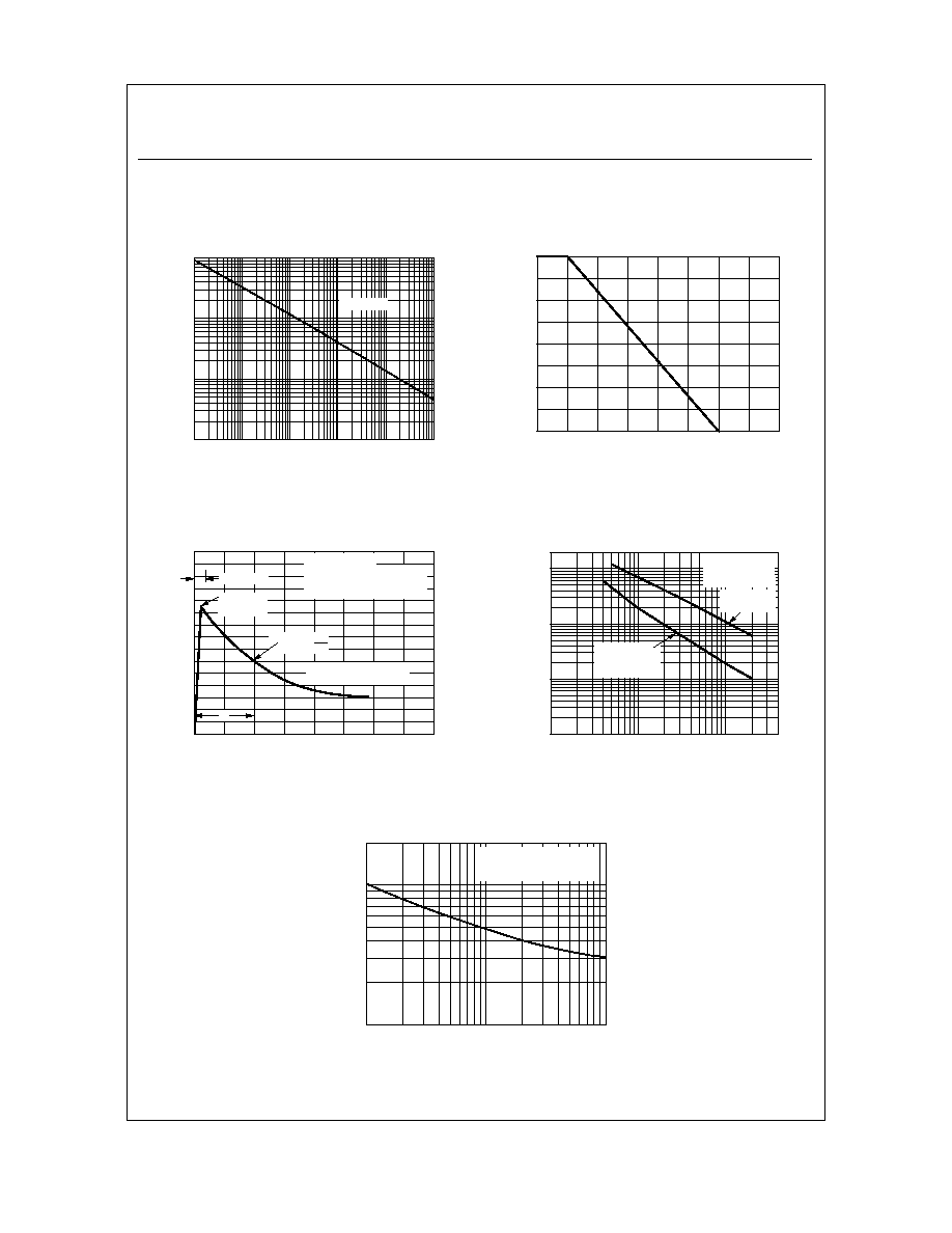
Typical Characteristics
Pulse Derating Curve
0
25
50
75
100
125
150
175
200
0
25
50
75
100
AMBIENT TEMPERATURE ( C)
PU
L
S
E
P
O
WE
R
(
%
)
º
Non-Repetitive Surge Current
1
2
5
10
20
50
100
10
20
50
100
200
NUMBER OF CYCLES AT 60Hz
F
O
R
W
A
R
D
S
URG
E
CU
RR
E
N
T
(
A
)
T = T max
8.3ms Single Half Sine-Wave
JEDEC Method
A
A
Peak Pulse Power Rating Curve
0.0001
0.001
0.01
0.1
1
10
0.1
1
10
100
PULSE WIDTH (ms)
P
U
LS
E PO
W
E
R
(
k
W
)
T = 25 C
º
A
Junction Capacitance
1
5
10
50
100 200 400
10
100
1000
10000
20000
REVERSE VOLTAGE (V)
C
A
PA
C
I
TA
N
C
E (
p
F
)
T = 25 C
º
A
f = 1.0 MHz
Visg = 50m Vp-p
Measured at
Zero Bias
Measured at
Stand-Off
Voltage (V mw)
Pulse Waveform
0
1
2
3
4
0
50
100
150
TIME (ms)
P
E
A
K
PU
LSE
C
U
RR
EN
T
(
%
)
T = 25 C
º
A
Pulse Width (td) is Defined
as the Point Where the Peak
Current Decays to 50% of Ipp
10/1000
µ
µ
µ
µ
sec Waveform
as Defined by R.E.A.
tf = 10
µ
µ
µ
µ
sec
e-kt
Peak Value
Ippm
Half Value-Ipp
2
td
DISCLAIMER
FAIRCHILD SEMICONDUCTOR RESERVES THE RIGHT TO MAKE CHANGES WITHOUT FURTHER
NOTICE TO ANY PRODUCTS HEREIN TO IMPROVE RELIABILITY, FUNCTION OR DESIGN. FAIRCHILD
DOES NOT ASSUME ANY LIABILITY ARISING OUT OF THE APPLICATION OR USE OF ANY PRODUCT
OR CIRCUIT DESCRIBED HEREIN; NEITHER DOES IT CONVEY ANY LICENSE UNDER ITS PATENT
RIGHTS, NOR THE RIGHTS OF OTHERS.
TRADEMARKS
The following are registered and unregistered trademarks Fairchild Semiconductor owns or is authorized to use and is
not intended to be an exhaustive list of all such trademarks.
LIFE SUPPORT POLICY
FAIRCHILD'S PRODUCTS ARE NOT AUTHORIZED FOR USE AS CRITICAL COMPONENTS IN LIFE SUPPORT
DEVICES OR SYSTEMS WITHOUT THE EXPRESS WRITTEN APPROVAL OF FAIRCHILD SEMICONDUCTOR CORPORATION.
As used herein:
1. Life support devices or systems are devices or
systems which, (a) are intended for surgical implant into
the body, or (b) support or sustain life, or (c) whose
failure to perform when properly used in accordance
with instructions for use provided in the labeling, can be
reasonably expected to result in significant injury to the
user.
2. A critical component is any component of a life
support device or system whose failure to perform can
be reasonably expected to cause the failure of the life
support device or system, or to affect its safety or
effectiveness.
PRODUCT STATUS DEFINITIONS
Definition of Terms
Datasheet Identification
Product Status
Definition
Advance Information
Preliminary
No Identification Needed
Obsolete
This datasheet contains the design specifications for
product development. Specifications may change in
any manner without notice.
This datasheet contains preliminary data, and
supplementary data will be published at a later date.
Fairchild Semiconductor reserves the right to make
changes at any time without notice in order to improve
design.
This datasheet contains final specifications. Fairchild
Semiconductor reserves the right to make changes at
any time without notice in order to improve design.
This datasheet contains specifications on a product
that has been discontinued by Fairchild semiconductor.
The datasheet is printed for reference information only.
Formative or
In Design
First Production
Full Production
Not In Production
ImpliedDisconnectTM
ISOPLANARTM
LittleFETTM
MicroFETTM
MicroPakTM
MICROWIRETM
MSXTM
MSXProTM
OCXTM
OCXProTM
OPTOLOGIC
OPTOPLANARTM
FACTTM
FACT Quiet SeriesTM
FAST
FASTrTM
FRFETTM
GlobalOptoisolatorTM
GTOTM
HiSeCTM
I
2
CTM
Rev. I3
ACExTM
ActiveArrayTM
BottomlessTM
CoolFETTM
CROSSVOLTTM
DOMETM
EcoSPARKTM
E
2
CMOS
TM
EnSigna
TM
PACMANTM
POPTM
Power247TM
PowerTrench
QFET
QSTM
QT OptoelectronicsTM
Quiet SeriesTM
RapidConfigureTM
RapidConnectTM
SILENT SWITCHER
SMART STARTTM
SPMTM
StealthTM
SuperSOTTM-3
SuperSOTTM-6
SuperSOTTM-8
SyncFETTM
TinyLogic
TruTranslationTM
UHCTM
UltraFET
VCXTM
Across the board. Around the world.TM
The Power FranchiseTM
Programmable Active DroopTM