 | –≠–ª–µ–∫—Ç—Ä–æ–Ω–Ω—ã–π –∫–æ–º–ø–æ–Ω–µ–Ω—Ç: RC6333 | –°–∫–∞—á–∞—Ç—å:  PDF PDF  ZIP ZIP |

www.fairchildsemi.com
Features
∑ Triple video amplifier
∑ 175 MHz -3 dB Bandwidth (A
V
= 2)
∑ 50 MHz
±
0.1 dB gain flatness
∑ Unity gain stable
∑ 0.06% differential gain (A
V
= 1, R
L
= 150
W
)
∑ 0.06
∞
differential phase (A
V
= 1, R
L
= 150
W
)
∑ High CMRR (95dB), High PSRR (80 dB)
∑ Dual
±
5V power supply
∑ Low offset 3.0 mV typical
∑ 14-pin narrow SO package
∑ 250V/
m
s slew rate
∑ Fast settling time: 0.1% in 15 ns
∑ TTL or CMOS compatible
Applications
∑ RGB amplifiers
∑ Video instrumentation amplifier
∑ Selectable gain amplifier
∑ Active filters
∑ Set-top Buffers/Drivers
Description
The RC6333 consists of three low power, wide band voltage
feedback operational amplifiers. Each channel is capable of
delivering a load current of at least 35mA.
The amplifiers are optimized for video applications where
low differential gain and low phase distortion are significant
requirements.
Block Diagram
65-3528-01
RC6333
OUT1
OUT3
OUT2
IN2-
IN2+
IN3+
IN3≠
≠
+
V
EE
IN1+
IN1≠
V
CC
≠
+
≠
+
RC6333
Triple Video Amplifier
Rev. 1.0.1

PRODUCT SPECIFICATION
RC6333
2
Pin Assignments
NC
RC6333
NC
NC
V
CC
IN1+
IN1≠
OUT1
OUT2
IN2≠
IN2+
V
EE
IN3+
IN3≠
OUT3
1
2
3
4
5
6
7
14
13
12
11
10
9
8
65-3528-02
Pin Definitions
Pin
Name
Pin
Number
Pin Function Description
IN1≠
6
Amplifier 1 inverting input
IN1+
5
Amplifier 1 non-inverting input
IN2≠
13
Amplifier 2 inverting input
IN2+
12
Amplifier 2 non-inverting input
IN3≠
9
Amplifier 3 inverting input
IN3+
10
Amplifier 3 non-inverting input
NC
1≠3
Not Connected.
OUT1
7
Amplifier 1 output
OUT2
14
Amplifier 2 output
OUT3
8
Amplifier 3 output
V
CC
4
Analog positive supply
V
EE
11
Analog negative supply
Absolute Maximum Ratings
(beyond which the device may be damaged)
1
Notes:
1. Functional operation under any of these conditions is NOT implied.
Operating Conditions
Parameter
Min
Typ
Max
Units
V
CC
Positive power supply
7
V
V
EE
Negative power supply
-7
V
Differential input voltage
10
V
Operating Temperature
0
+70
∞
C
Storage Temperature
-40
±
125
∞
C
Junction Temperature
150
∞
C
Lead Soldering (10 seconds)
240
∞
C
Short circuit tolerance:
No more than one output can be shorted to ground.
Parameter
Min
Typ
Max
Units
V
CC
Power Supply Voltage
4.75
5.0
5.25
V
V
EE
Negative Supply Voltage
-4.75
-5.0
-5.25
V
q
JA
SO14 Thermal Resistance
105
∞
C/W

RC6333
PRODUCT SPECIFICATION
3
DC Characteristics
V
CC
= 5V, V
EE
= -5V, A
V
= 2, R
LOAD
= 150
W
, T
A
= 0
∞
C to 70
∞
C, unless otherwise specified. Open Loop.
Note:
1. Guaranteed by design.
AC Characteristics
V
CC
= 5V, V
EE
= -5V, A
V
= 2, T
A
= 0 to 70
∞
C, R
LOAD
= 150
W
, R
G
= R
F
= 250
W
,
C
L
= 10 pF, unless otherwise specified. Closed Loop. Guaranteed by Design. See Typical Test Circuit.
Parameter
Conditions
Min
Typ
Max
Units
V
OS
Input Offset Voltage
No Load
3
±
10
mV
D
V
OS
/
D
T Offset Voltage Drift
1
±
6
±
30
m
V/
∞
C
I
B
Input Bias Current
±
1
±
5
m
A
D
I
B
/
D
T
Input Bias Current Drift
1
±
8
±
40
nA/
∞
C
Rin
Input Resistance
1
1
M
W
Cin
Input Capacitance
1
0.5
2
pF
CMIR
Common Mode Input Range
±
2.5
V
CMRR
Common Mode Rejection Ratio
No Load
70
100
dB
PSRR
Power Supply Rejection Ratio
No Load
65
80
dB
Is
Quiescent Supply Current
No Load
26
40
mA
R
OUT
Output Impedance (Closed Loop)
1
Enabled, At DC
0.2
W
I
OUT
Output Current
Per Amplifier
35
mA
V
OUT
Output Voltage Swing
No Load
±
2.5
±
3.0
V
R
L
= 150
W
±
2.5
±
3.0
V
A
VOL
Open-loop Gain
60
75
dB
Parameter
Conditions
Min
Typ
Max
Units
Frequency Response
BW
-3 dB Bandwidth (A
V
= 2)
V
OUT
= 0.4 Vpp
+175
MHz
V
OUT
= 0.8 Vpp
75
90
MHz
Flat
±
0.1 dB Bandwidth
V
OUT
= 0.4 Vpp
50
75
MHz
Peak
Maximum Small Signal AC
Peaking
V
OUT
= 0.8 Vpp
0.01
dB
X
TALK
Crosstalk Isolation
@ 5 MHz
50
dB
Time Domain Response
t
r1
, t
f1
Rise and Fall Time 10% to 90%
2V Output Step
10
15
ns
ts
Settling Time to 0.1%
2V Output Step
15
ns
OS
Overshoot
2V Output Step
5
%
US
Undershoot
2V Output Step
2
%
SR
Slew Rate
V
OUT
=
±
2.0V
200
250
V/
m
s
Distortion
HD
2
2nd Harmonic Dist. @ 20 MHz
V
OUT
= 0.8 Vpp
-48
dB
HD
3
3nd Harmonic Dist. @ 20 MHz
V
OUT
= 0.8 Vpp
-56
dB
Video Performance
DG
Diff. Gain (p-p), NTSC & PAL
R
L
= 150
W
, V
OUT
=
±
1.5V
0.06
%
DP
Diff. Phase (p-p), NTSC & PAL
R
L
= 150
W
, V
OUT
=
±
1.5V
0.06
Deg.
NF
Noise Floor
>100kHz
-130
dB rms
PRODUCT SPECIFICATION
RC6333
4
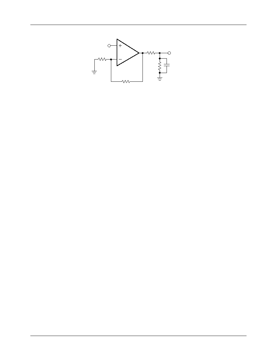
Test Circuit
65-3528-04
1/3
RC6333
10 pF
C
L
75
W
R
L
75
W
Video
Output
R
F
250
W
250
W
Video
Input
R
G
R
S
R
LOAD
= R
L
+ R
S
Applications Discussion
Capacitive Load
The RC6333 can drive a capacitive load from 10 to over 50
pF. In back terminated video applications, bandwidth will
only be limited by the RC time constants of the external out-
put components. When driving a 75
W cable, place the 75W
source termination resistor as close to the amplifier output as
possible.
DC Accuracy
Since the RC6333 is a voltage-feedback amplifier, the invert-
ing and non-inverting inputs have similar impedances and
bias currents. To minimize offset voltage, match the source
resistances seen by inverting and non-inverting inputs.
Feedback Components
Because the RC6333 is a voltage-feedback amplifier, it facil-
itates using reactive (capacitive and inductive) feedback
components for implementing filters, integrators, sample/
hold circuits, etc. The feedback network and the parasitic
capacitance at the inverting (summing junction) input create
a pole and affect the transfer function of the circuit. For sta-
ble operation, minimize the parasitic capacitance and equiva-
lent resistance of the components used in the feedback
circuit.
Circuit Board
High-frequency applications require good grounding, power
supply decoupling, low parasitic capacitance and inductance,
and good isolation between the inputs to minimize their
crosstalk. Avoid coupling from output to input to prevent
positive feedback.

RC6333
PRODUCT SPECIFICATION
5
Notes: