 | ÐлекÑÑоннÑй компоненÑ: ML2004 | СкаÑаÑÑ:  PDF PDF  ZIP ZIP |
Äîêóìåíòàöèÿ è îïèñàíèÿ www.docs.chipfind.ru
www.fairchildsemi.com
REV. 1.1.1 3/19/01
Features
· Low noise: 0 dBrnc max with +24dB gain
· Low harmonic distortion: -60dB max
· Gain range: 24 to +24dB
· Resolution: 0.1dB steps
· Flat frequency response:
±0.05dB from .34 kHz
±0.10dB from .1-20 kHz
· Low supply current 4mA max from ±5V supplies
· TTL/CMOS compatible digital interface
· ML2003 has pin selectable serial or parallel interface;
ML2004 serial interface only
General Description
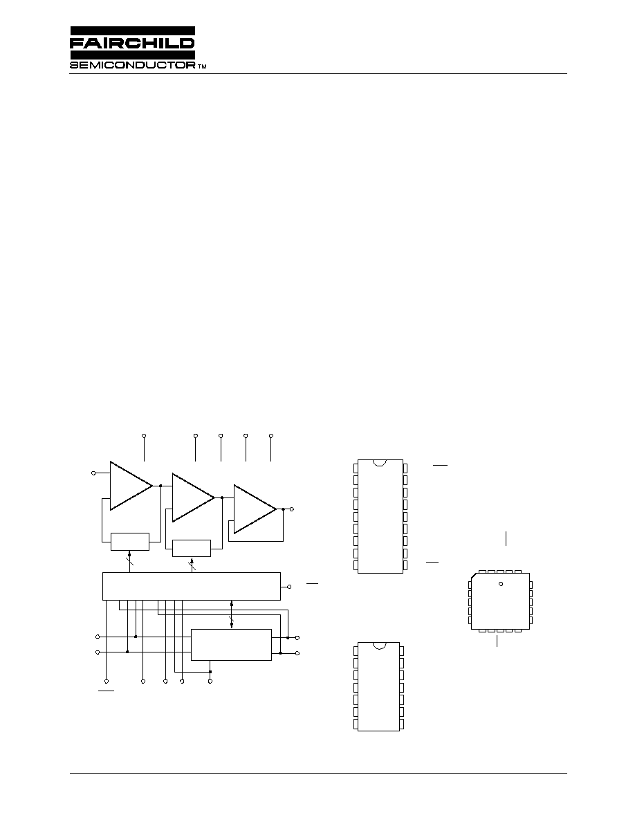
The ML2003 and ML2004 are digitally controlled logarith-
mic gain/attenuators with a range of 24 to +24 dB in 0.1 dB
steps.
The gain settings are selected by a 9-bit digital word.
The ML2003 digital interface is either parallel or serial.
The ML2004 is packaged in a 14-pin DIP with a serial
interface only.
Absolute gain accuracy is 0.05dB max over supply tolerance
of ±10% and temperature range.
These CMOS logarithmic gain/attenuators are designed for a
wide variety of applications in telecom, audio, sonar, or gen-
eral purpose function generation. One specific intended
application is analog telephone lines.
Block Diagram
Pin Connections
V
OUT
V
IN
V
CC
P
DN
A GND
V
SS
GND
+
16
16
C0
C1
F0
F2
9
C2
C3
F1
F3
F2
(SCK)
C2
(LATI)
ATTEN/
GAIN
C1
(SID)
C0
(LATO)
F0
(SOD)
C3
(LATI)C2
(SID)C1
C0 (LATO)
NC
P
DN
F3
F2 (SCK)
V
OUT
V
SS
A GND
NC
NC
(LATO)C0
P
DN
F3
(SCK)F2
F1
GND
C1 (SID)
F1
GND
SER/P
AR
F0 (SOD)
V
IN
C2 (LA
TI)
C3
A
TTEN/GAIN
V
CC
1
4
5
6
7
8
18
17
16
15
14
1 20 19
2
3
11 12 13
10
9
2
3
4
5
6
7
8
9
18
17
16
15
14
13
12
11
10
ATTEN/GAIN
ML2003
18-PIN DIP
20-Pin PCC
ML2003
TOP VIEW
TOP VIEW
V
CC
V
OUT
V
SS
A GND
V
IN
NC
F0 (SOD)
SER/PAR
COURSE
DECODER/MODE SELECTOR
9-BIT LATCH &
SHIFT REGISTER
RESISTORS/
SWITCHES
NOTE: SERIAL MODE FUNCTIONS INDICATED BY PARENTHESES.
RESISTORS/
SWITCHES
+
FINE
+
BUFFER
SER/PAR
LATI
SID
LATO
P
DN
NC
SCK
GND
1
2
3
4
5
6
7
14
13
12
11
10
9
8
ML2004
14-PIN DIP
TOP VIEW
V
CC
V
OUT
V
SS
A GND
V
IN
NC
SOD
ML2003, ML2004
Logarithmic Gain/Attenuator
ML2003, ML2004
PRODUCT SPECIFICATION
2
REV. 1.1.1 3/19/01
Pin Description
Absolute Maximum Ratings
1
Name
Function
C3
In serial mode, pin is unused. In parallel mode, coarse gain select bit. Pin has internal pulldown
resistor to GND.
(LATI) C2
In serial mode, input latch clock which loads the data from the shift register into the latch.
In parallel mode, coarse gain select bit. Pin has internal pulldown resistor to GND.
(SID) C1
In serial mode, serial data input that contains serial 9 bit data word which controls the gain
setting. In parallel mode, coarse gain select bit. Pin has internal pulldown resistor to GND.
(LATO) C0
In serial mode, output latch clock which loads the 9 bit data word back into the shift register from
the latch. In parallel mode, coarse gain select bit. Pin has internal pulldown resistor to GND.
P
DN
Powerdown input
. When P
DN
= 1, device is in powerdown mode. When P
DN
= 0, device is in
normal operation. Pin has internal pulldown resistor to GND.
F3
In serial mode, pin is unused. In parallel mode, fine gain select bit. Pin has internal pulldown
resistor to GND.
(SCK) F2
In serial mode, shift register clock which shifts the serial data on SID into the shift register on
rising edges and out on SOD on falling edges. In parallel mode, fine gain select bit. Pin has
internal pulldown resistor to GND.
F1
In serial mode, pin is unused. In parallel mode, fine gain select bit. Pin has internal pulldown
resistor to GND.
GND
Digital ground
. 0 volts. All digital inputs and outputs are referenced to this ground.
SER/PAR
Serial or parallel select input. When SER/PAR = 1, device is in serial mode.
When SER/PAR = 0, device is in parallel mode. Pin has internal pullup resistor to V
CC
.
(SOD) F0
In serial mode, serial output data which is the output of the shift register. In parallel mode, fine
gain select bit. Pin has internal pulldown resistor to GND.
V
IN
Analog input
.
AGND
Analog ground
. 0 volts. Analog input and output are referenced to this ground.
V
SS
Negative supply
. 5 volts ±10%.
V
OUT
Analog output
.
V
CC
Positive supply
. +5 volts ±10%.
ATTEN/GAIN
In serial mode, pin is unused. In parallel mode, attenuation/gain select bit. Pin has internal
pulldown resistor to GND.
Parameter
Min.
Max.
Units
Supply Voltage
V
CC
V
SS
+6.5
-6.5
V
V
AGND with respect to GND
±0.5
V
Analog Input and Output
V
SS
0.3V
V
CC
+0.3
V
Digital Input and Outputs
GND 0.3
V
CC
+0.3
V
Input Current Per Pin
±25
mA
Power Dissipation
750
mW
Storage Temperature Range
-65
+150
°C
Lead Temeperature (Soldering, 10 sec)
300
°C
PRODUCT SPECIFICATION
ML2003, ML2004
REV. 1.1.1 3/19/01
3
Operating Conditions
Parameter
Min.
Max.
Units
Temperature Range
2
ML2003CX, ML2004CX
ML2003IX, ML2004IX
0
-40
70
85
°C
°C
Supply Voltage
V
CC
V
SS
4
-4
6
-6
V
V
Electrical Characteristics
Unless otherwise specified T
A
= T
MIN
to T
MAX
, V
CC
= 5V ± 10%, V
SS
= -5V ±10%, Data Word: ATTEN/GAIN = 1,
Other Bits = 0(0dB Ideal Gain), C
L
= 100pF, R
L
= 600
, SCK = LATI = LATO = 0, dBm measurements use 600
as
reference load, digital timing measured at 1.4 V, C
L
= 100pF or SOD.
Symbol
Parameter
Notes
Conditions
Min. Typ.
3
Max. Units
Analog
AG
Absolute gain
accuracy
4
V
IN
=8dBm, 1 kHz
-0.05
+0.05
dB
RG
Relative gain
accuracy
4 100000001
000000000
000000001
All other gain settings
All values referenced to 100000000 gain
when ATTEN/GAIN = 1, V
IN
=8dBm when
ATTEN//GAIN =0
V
IN
=(8dBm Ideal Gain) in dB
-0.05
-0.05
-0.05
-0.1
+0.05
+0.05
+0.05
+0.1
dB
dB
dB
dB
FR
Frequency response
4
300-4000 Hz
100-20,000 Hz
Relative to 1 kHz
-0.05
-0.1
+0.05
+0.1
dB
dB
VOS
Output Offset Voltage
4
V
IN
= 0, +24dB gain
±100
mV
ICN
Idle Channel Noise
4
5
V
IN
= 0, +24dB gain, C msg. Weighted
V
IN
= 0, +24dB gain, 1kHz
-6
450
0
900
dBrnc
nv/
Hz
HD
Harmonic Distortion
4
V
IN
= 8dBm gain, 1kHz Measure 2nd,
3rd harmonic relative to fundamental
-60
dB
SD
Signal to Distortion
4
V
IN
= 8dBm, 1 kHz
C msg. weighted
+60
dB
PSRR
Power Supply
Rejection
4
200mVp-p, 1 kHz sine, V
IN
= 0
on V
CC
on V
SS
-60
-60
-40
-40
dB
dB
Z
IN
Input impedance, V
IN
4
1
Meg
V
INR
Input Voltage Range
4
±3.0
V
V
OSW
Output Voltage Swing
4
±3.0
V
Digital and DC
V
IL
Digital Input Low
Voltage
4
0.8
V
V
IH
Digital Input High
Voltage
4
2.0
V
V
OL
Digital Output Low
Voltage
4
I
OL
= 2mA
0.4
V
ML2003, ML2004
PRODUCT SPECIFICATION
4
REV. 1.1.1 3/19/01
Notes:
1. Absolute maximum ratings are limits beyond which the life of the integrated circuit may be impaired. All voltages unless
otherwise specified are measured with respect to ground.
2. 0°C to +70°C and 40°C to +85°C operating temperature range devices are 100% tested with temperature limits guaranteed
by 100% testing, sampling, or by correlation with worst-case test conditions.
3. Typicals are parametric norm at 25°C.
4. Parameter guaranteed and 100% production tested.
5. Parameter guaranteed. Parameters not 100% tested are not in outgoing quality level calculation.
V
OH
Digital Output High
Voltage
4
I
OH
= -1mA
4.0
V
I
NS
Input Current, SER/
PAR
4
V
IH
= GND
-5
-100
µA
I
ND
Input Current,
All Digital Inputs
Except SER/PER
4
V
IH
= V
CC
5
100
µA
I
CC
V
CC
Supply Current
4
No output load, V
IL
= GND,
V
IH
= V
CC
, V
IN
= 0
4
mA
I
SS
V
SS
Supply Current
4
No output load, V
IL
= GND,
V
IH
= V
CC
, V
IN
= 0
-4
mA
I
CCP
V
CC
Supply Current,
Powerdown Mode
4
No output load, V
IL
= GND,
V
IH
= V
CC
0.5
mA
I
SSP
V
SS
Supply Current
Powerdown Mode
4
No output load, V
IL
= GND,
V
IH
= V
CC
-0.1
mA
AC Characteristics
t
SET
V
OUT
Settling Time
4
V
IN
= 0.185V. Change gain from 24 to
+24dB. Measure from LATI rising edge to
when V
OUT
settles to within 0.05dB of final
value.
20
µs
t
STEP
V
OUT
Step Response
4
Gain = +24dB. V
IN
= -0.185 to +0.185V
step. Measure when V
OUT
settles to within
0.05dB of final value.
20
µs
t
SCK
SCK On/Off Period
4
250
ns
t
S
SID Data Setup Time
4
50
ns
t
H
SID Data Hold Time
4
50
ns
t
D
SOD Data Delay
4
0
125
ns
t
IPW
LATI Pulse Width
4
50
ns
t
OPW
LATO Pulse Width
4
50
ns
t
IS
, t
OS
LATI, LATO Setup
Time
4
50
ns
t
IH
,
t
OH
LATI, LATO Hold
Time
5
50
ns
t
PLD
SOD Parallel Load
Delay
4
0
125
ns
Electrical Characteristics
(continued)
Unless otherwise specified T
A
= T
MIN
to T
MAX
, V
CC
= 5V ± 10%, V
SS
= -5V ±10%, Data Word: ATTEN/GAIN = 1,
Other Bits = 0(0dB Ideal Gain), C
L
= 100pF, R
L
= 600
, SCK = LATI = LATO = 0, dBm measurements use 600 as
reference load, digital timing measured at 1.4 V, C
L
= 100pF or SOD.
Symbol
Parameter
Notes
Conditions
Min. Typ.
3
Max. Units
PRODUCT SPECIFICATION
ML2003, ML2004
REV. 1.1.1 3/19/01
5
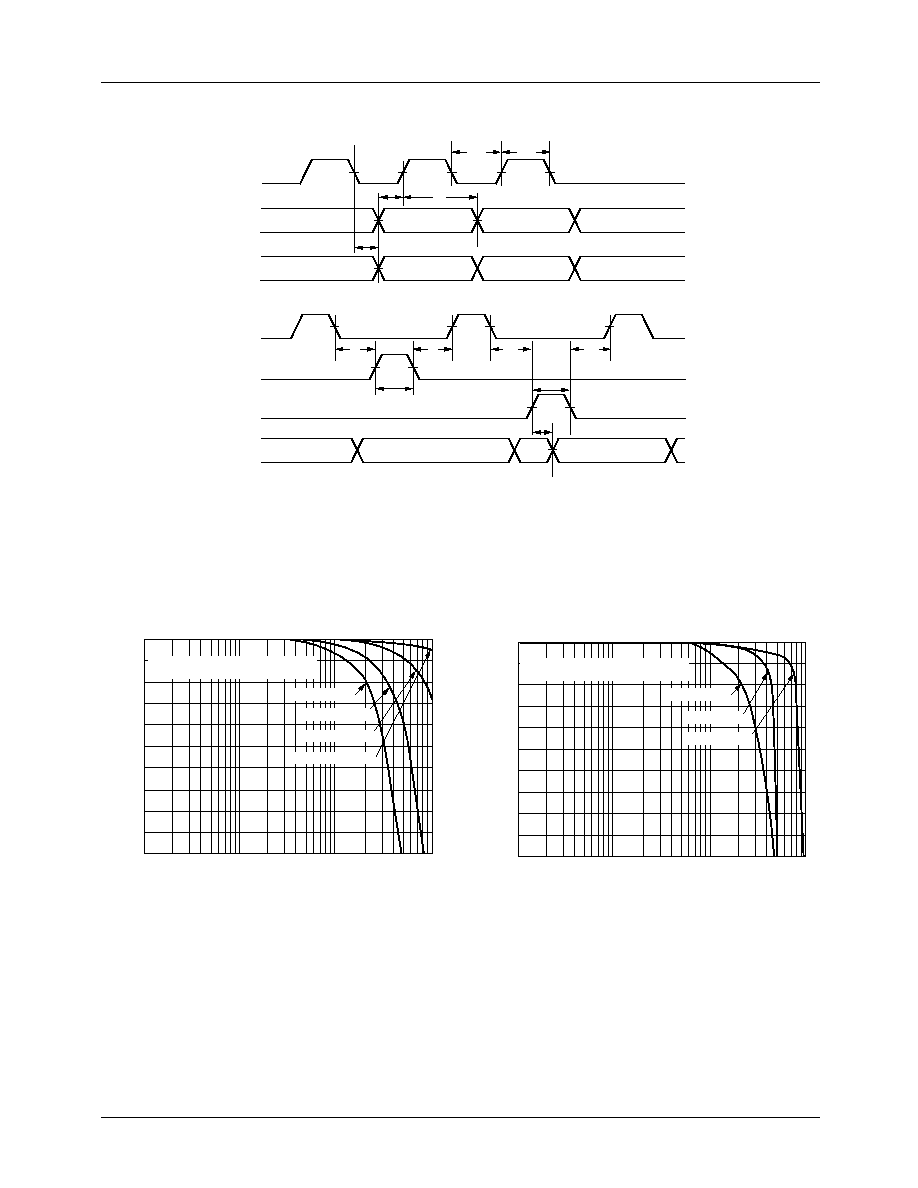
Timing Diagram
Figure 1. Serial Mode Timing Diagram
SCK
t
SCK
t
SCK
t
S
t
IS
t
IH
t
OS
t
OH
t
IPW
t
OPW
t
PLD
t
D
t
H
SID
SOD
SCK
LATI
LATO
SOD
TIMING PARAMETERS ARE REFERENCED TO THE 1.4 VOLT MIDPOINT.
Typical Performance Curves
Figure 2. Amplitude vs Frequency (V
IN
/V
OUT
= .5V
RMS
)
Figure 3. Amplitude vs Frequency (V
IN
/V
OUT
= 2V
RMS
)
0
0
-0.5
AMPLITUDE (dB)
FREQUENCY (Hz)
-0.10
-0.15
-0.20
-0.25
-0.30
-0.35
-0.40
-0.45
-0.50
100
1K
10K
100K
-0.5
AMPLITUDE (dB)
FREQUENCY (Hz)
-0.10
-0.15
-0.20
-0.25
-0.30
-0.35
-0.40
-0.45
-0.50
100
1K
10K
100K
ATTEN: V
IN
= 0.5V
RMS
GAIN: V
IN
= 0.5V
RMS
/GAIN SETTING
ATTEN: V
IN
= 2V
RMS
GAIN: V
IN
= 2V
RMS
/GAIN SETTING
GAIN = +24dB
GAIN = +18dB
GAIN = +12dB
GAIN = +0, -24dB
GAIN = +24dB
GAIN = 0dB
GAIN = 24dB