 | ÐлекÑÑоннÑй компоненÑ: DM74S161 | СкаÑаÑÑ:  PDF PDF  ZIP ZIP |
Äîêóìåíòàöèÿ è îïèñàíèÿ www.docs.chipfind.ru
© 2000 Fairchild Semiconductor Corporation
DS006471
www.fairchildsemi.com
August 1986
Revised April 2000
DM74S161 · D
M
74S163
Synchr
onous 4-Bi
t Binar
y
Count
ers
DM74S161 · DM74S163
Synchronous 4-Bit Binary Counters
General Description
These synchronous, presettable counters feature an inter-
nal carry look-ahead for application in high-speed counting
designs. They are 4-bit binary counters. The carry output is
decoded by means of a NOR gate, thus preventing spikes
during the normal counting mode of operation. Synchro-
nous operation is provided by having all flip-flops clocked
simultaneously so that the outputs change coincident with
each other when so instructed by the count enable inputs
and internal gating. This mode of operation eliminates the
output counting spikes which are normally associated with
asynchronous (ripple clock) counters. A buffered clock
input triggers the four flip-flops on the rising (positive-
going) edge of the clock input waveform.
These counters are fully programmable; that is, the outputs
may be preset to either level. As presetting is synchronous,
setting up a LOW level at the load input disables the
counter and causes the outputs to agree with the setup
data after the next clock pulse regardless of the levels of
the enable input.
The carry look-ahead circuitry provides for cascading
counters for n-bit synchronous applications without addi-
tional gating. Instrumental in accomplishing this function
are two count-enable inputs and a ripple carry output. Both
count-enable inputs (P and T) must be HIGH to count, and
input T is fed forward to enable the ripple carry output. The
ripple carry output thus enabled will produce a HIGH-level
output pulse with a duration approximately equal to the
HIGH-level portion of the Q
A
output. This HIGH-level over-
flow ripple carry pulse can be used to enable successive
cascaded stages.
Features
s
Synchronously programmable
s
Internal look-ahead for fast counting
s
Carry output for n-bit cascading
s
Synchronous counting
s
Load control line
s
Diode-clamped inputs
Ordering Code:
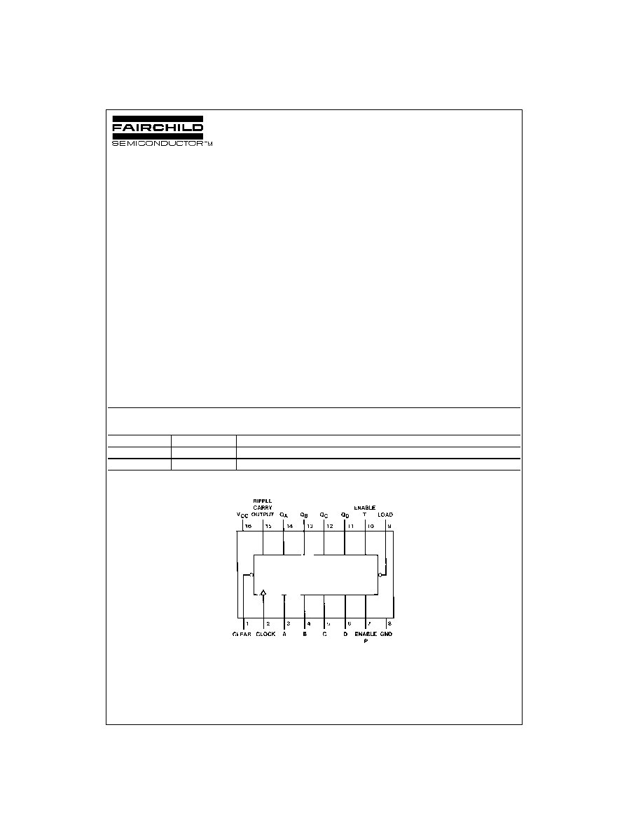
Connection Diagram
Order Number
Package Number
Package Description
DM74S161N
N16E
16-Lead Plastic Dual-In-Line Package (PDIP), JEDEC MS-001, 0.300 Wide
DM74S163N
N16E
16-Lead Plastic Dual-In-Line Package (PDIP), JEDEC MS-001, 0.300 Wide
www.fairchildsemi.com
2
DM74S161
·
D
M
74S163
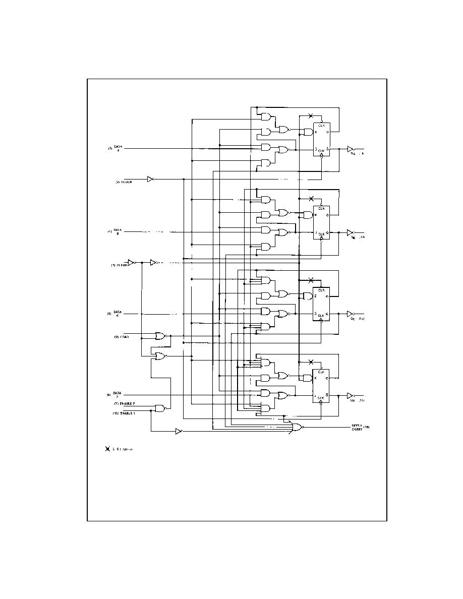
Logic Diagram
DM74S161 · DM74S163
3
www.fairchildsemi.com
DM74S161
·
D
M
74S163
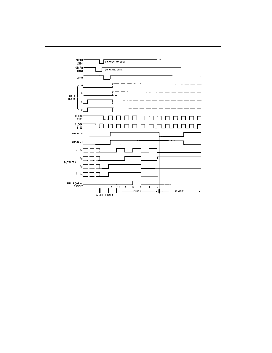
Timing Diagram
Sequence:
1. Clear outputs to zero
2. Preset to binary twelve
3. Count to thirteen, fourteen, fifteen, zero, one and two
4. Inhibit
www.fairchildsemi.com
4
DM74S161
·
D
M
74S163
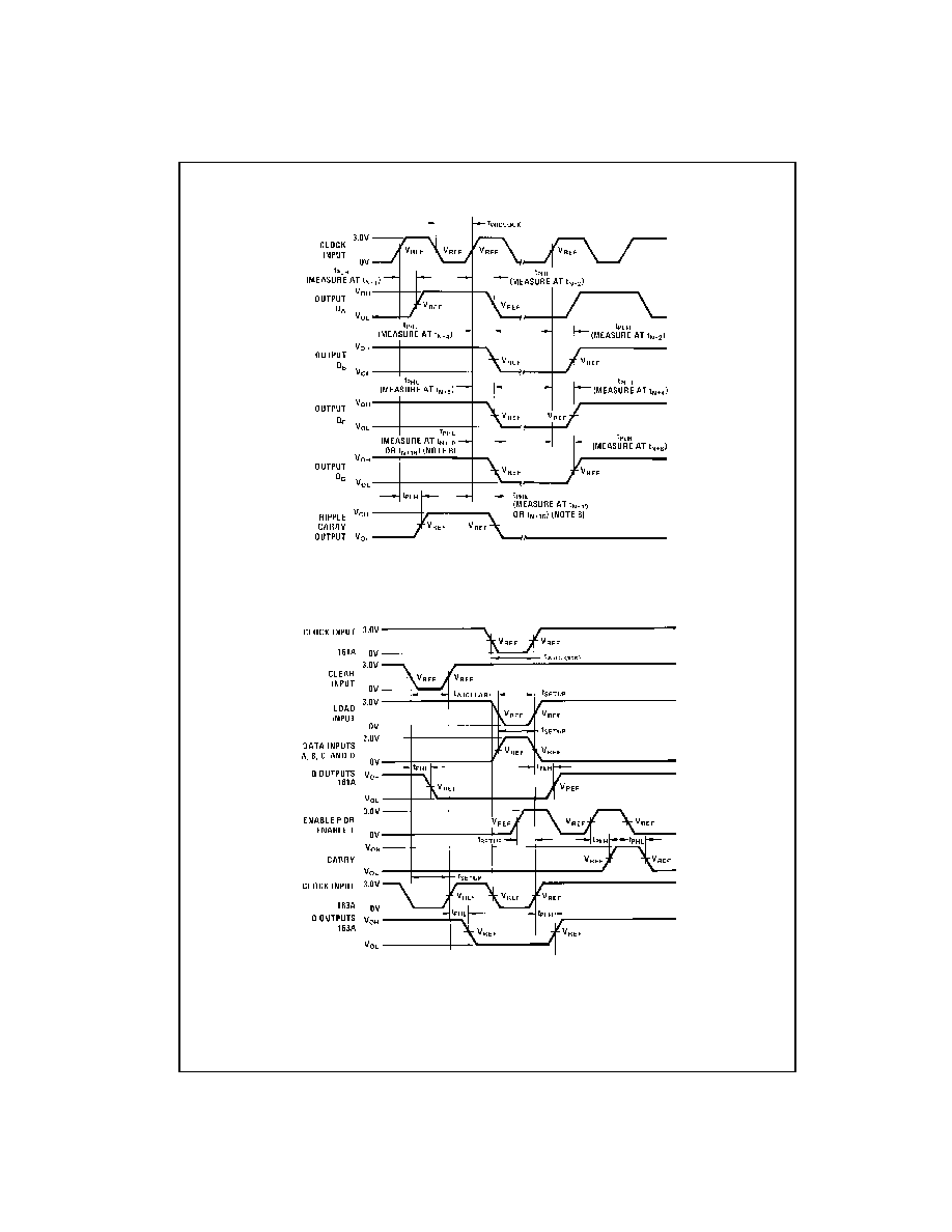
Parameter Measurement Information
Switching Time Waveforms
Note A:The input pulses are supplied by generators having the following characteristics:
PRR
1 MHz, duty cycle
50%, Z
OUT
50
. For DM74S161/163, t
r
2.5 ns, t
f
2.5 ns. Vary PRR to measure f
MAX
.
Note B: Outputs Q
D
and carry are tested at t
n
+
16 for DM74S161, SM74S163 where t
n
is the bit time when all outputs are LOW
Note C: V
REF
=
1.5V.
Switching Time Waveforms
Note A: The input pulses are supplied by generators having the following characteristics:
PRR
1 MHz, duty cycle
50%, Z
OUT
50
. t
r
2.5 ns, t
f
2.5 ns. Vary PRR to measure f
MAX
.
Note B: Enable P and enable T setup times are measured at t
n
+
0.
Note C:V
REF
=
1.5V.
5
www.fairchildsemi.com
DM74S161
·
D
M
74S163
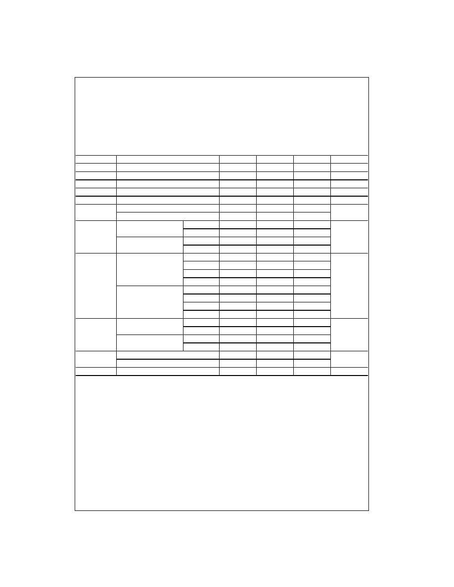
Absolute Maximum Ratings
(Note 1)
Note 1: The "Absolute Maximum Ratings" are those values beyond which
the safety of the device cannot be guaranteed. The device should not be
operated at these limits. The parametric values defined in the Electrical
Characteristics tables are not guaranteed at the absolute maximum ratings.
The "Recommended Operating Conditions" table will define the conditions
for actual device operation.
Recommended Operating Conditions
Note 2: C
L
=
15 pF, R
L
=
280
, T
A
=
25
°
C and V
CC
=
5V.
Note 3: C
L
=
50 pF, R
L
=
280
, T
A
=
25
°
C and V
CC
=
5V.
Note 4: Applies only to the DM74S163 which has synchronous clear inputs.
Note 5: Applies only to the DM74S161 which has asynchronous clear inputs.
Supply Voltage
7V
Input Voltage
5.5V
Operating Free Air Temperature Range
0
°
C to
+
70
°
C
Storage Temperature Range
-
65
°
C to
+
150
°
C
Symbol
Parameter
Min
Nom
Max
Units
V
CC
Supply Voltage
4.75
5
5.25
V
V
IH
HIGH Level Input Voltage
2
V
V
IL
LOW Level Input Voltage
0.8
V
I
OH
HIGH Level Output Current
-
1
mA
I
OL
LOW Level Output Current
20
mA
f
CLK
Clock Frequency (Note 2)
0
40
MHz
Clock Frequency (Note 3)
0
35
t
W
Pulse Width (Note 2)
Clock
10
ns
Clear (Note 5)
10
Pulse Width (Note 3)
Clock
12
Clear (Note 5)
12
t
SU
Setup Time (Note 2)
Data
4
ns
Enable P or T
12
Load
14
Clear (Note 4)
14
Setup Time (Note 3)
Data
5
Enable P or T
14
Load
16
Clear (Note 4)
16
t
H
Hold Time (Note 2)
Data
3
ns
Others
0
Hold Time (Note 3)
Data
5
Others
2
t
REL
Load or Clear Release Time (Note 2)
12
ns
Load or Clear Release Time (Note 3)
14
T
A
Free Air Operating Temperature
0
70
°
C