 | –≠–ª–µ–∫—Ç—Ä–æ–Ω–Ω—ã–π –∫–æ–º–ø–æ–Ω–µ–Ω—Ç: DM74AS280 | –°–∫–∞—á–∞—Ç—å:  PDF PDF  ZIP ZIP |

© 2000 Fairchild Semiconductor Corporation
DS006303
www.fairchildsemi.com
October 1986
Revised March 2000
DM74AS280 9-
B
i
t Pari
ty
Gener
ator
/Checker
DM74AS280
9-Bit Parity Generator/Checker
General Description
These universal, 9-bit parity generators/checkers utilize
advanced Schottky high performance circuitry and feature
odd/even outputs to facilitate operation of either odd or
even parity applications. The word length capability is eas-
ily expanded by cascading.
The DM74AS280 can be used to upgrade the performance
of most systems utilizing the '180 parity generator/checker.
Although the DM74AS280 is implemented without
expander inputs, the corresponding function is provided by
the availability of an input at pin 4 and no internal connec-
tion at pin 3. This permits the DM74AS280 to be substi-
tuted for the '180 in existing designs to produce identical
function even if DM74AS280s are mixed with existing
'180s.
Features
s
Generates either odd or even parity for nine data lines
s
Inputs are buffered to lower the drive requirements
s
Can be used to upgrade existing systems using MSI
parity circuits
s
Cascadable for N-bits
s
Advanced oxide-isolated, ion-implanted Schottky
TTL process
s
Switching specifications at 50 pF
s
Switching specifications guaranteed over full
temperature and V
CC
range
Ordering Code:
Devices also available in Tape and Reel. Specify by appending the suffix letter "X" to the ordering code.
Connection Diagram
Function Table
L
=
LOW State
H
=
HIGH State
Order Number
Package Number
Package Description
DM74AS280M
M14A
14-Lead Small Outline Integrated Circuit (SOIC), JEDEC MS-012, 0.150 Narrow
DM74AS280N
N14A
14-Lead Plastic Dual-In-Line Package (PDIP), JEDEC MS-001, 0.300 Wide
Number of Inputs (A thru I)
Outputs
that are HIGH
Even
Odd
0, 2, 4, 6, 8
H
L
1, 3, 5, 7, 9
L
H

www.fairchildsemi.com
2
DM
74AS280
Logic Diagram
3
www.fairchildsemi.com
DM74AS280
Absolute Maximum Ratings
(Note 1)
Note 1: The "Absolute Maximum Ratings" are those values beyond which
the safety of the device cannot be guaranteed. The device should not be
operated at these limits. The parametric values defined in the Electrical
Characteristics tables are not guaranteed at the absolute maximum ratings.
The "Recommended Operating Conditions" table will define the conditions
for actual device operation.
Recommended Operating Conditions
Electrical Characteristics
Over recommended free-air temperature range. All typical values are measured at V
CC
=
5V, T
A
=
25
∞
C.
Switching Characteristics
over recommended operating free air temperature range
Supply Voltage
7V
Input Voltage
7V
Operating Free Air Temperature Range
0
∞
C to
+
70
∞
C
Storage Temperature Range
-
65
∞
C to
+
150
∞
C
Typical
JA
N Package
77.0
∞
C/W
M Package
108.0
∞
C/W
Symbol
Parameter
Min
Typ
Max
Units
V
CC
Supply Voltage
4.5
5
5.5
V
V
IH
HIGH Level Input Voltage
2
V
V
IL
LOW Level Input Voltage
0.8
V
I
OH
HIGH Level Output Current
-
2
mA
I
OL
LOW Level Output Current
20
mA
T
A
Free-Air Operating Temperature
0
70
∞
C
Symbol
Parameter
Conditions
Min
Typ
Max
Units
V
IK
Input Clamp Voltage
V
CC
=
4.5V, I
I
=
-
18 mA
-
1.2
V
V
OH
HIGH Level Output Voltage
I
OH
=
-
2 mA, V
CC
=
4.5V to 5.5V
V
CC
-
2
V
V
OL
LOW Level Output Voltage
V
CC
=
4.5V, I
OL
=
Max
0.35
0.5
V
I
I
Input Current @ Max Input Voltage
V
CC
=
5.5V, V
IH
=
7V
0.1
mA
I
IH
HIGH Level Input Current
V
CC
=
5.5V, V
IH
=
2.7V
20
µ
A
I
IL
LOW Level Input Current
V
CC
=
5.5V, V
IL
=
0.4V
-
0.5
mA
I
O
Output Drive Current
V
CC
=
5.5V, V
O
=
2.25V
-
30
-
112
mA
I
CC
Supply Current
V
CC
=
5.5V
25
40
mA
Symbol
Parameter
Conditions
From
To Min
Max
Units
t
PLH
Propagation Delay Time,
V
CC
=
4.5V to 5.5V,
Data
Even
3
12
ns
LOW-to-HIGH Level Output
C
L
=
50 pF,
t
PHL
Propagation Delay Time,
R
L
=
500
3
11
ns
HIGH-to-LOW Level Output
t
PLH
Propagation Delay Time,
Data
Odd
3
12
ns
LOW-to-HIGH Level Output
t
PHL
Propagation Delay Time,
3
11.5
ns
HIGH-to-LOW Level Output

www.fairchildsemi.com
4
DM
74AS280
Typical Applications
Three DM74AS280s can be used to implement a 25-line
parity generator/checker.
As an alternative, the outputs of two or three parity genera-
tors/checkers can be decoded with a 2-input (AS86) or 3-
input (S135) exclusive-OR gate for 18 or 27-line parity
applications.
Longer word lengths can be implemented by cascading
DM74AS280s. As shown in Figure 2, parity can be gener-
ated for word lengths up to 81 bits.
FIGURE 1. 25-Line
Parity/Generator Checker
FIGURE 2. 81-Line Parity/Generator Checker

5
www.fairchildsemi.com
DM74AS280
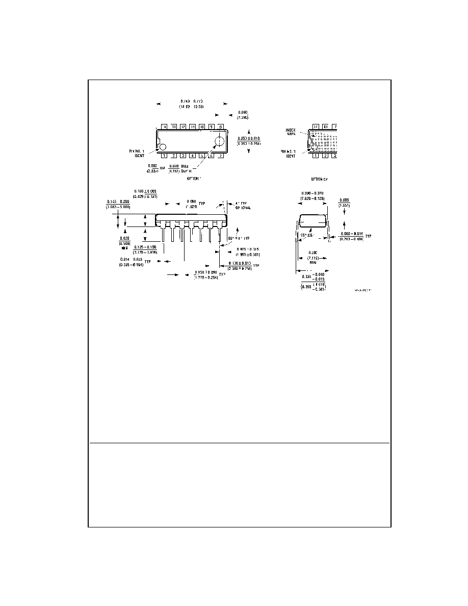
Physical Dimensions
inches (millimeters) unless otherwise noted
14-Lead Small Outline Integrated Circuit (SOIC), JEDEC MS-012, 0.150 Narrow
Package Number M14A
www.fairchildsemi.com
6
DM74AS280 9-Bi
t Pari
ty Generat
or/
C
hecker
Physical Dimensions
inches (millimeters) unless otherwise noted (Continued)
14-Lead Plastic Dual-In-Line Package (PDIP), JEDEC MS-001, 0.300 Wide
Package Number N14A
Fairchild does not assume any responsibility for use of any circuitry described, no circuit patent licenses are implied and
Fairchild reserves the right at any time without notice to change said circuitry and specifications.
LIFE SUPPORT POLICY
FAIRCHILD'S PRODUCTS ARE NOT AUTHORIZED FOR USE AS CRITICAL COMPONENTS IN LIFE SUPPORT
DEVICES OR SYSTEMS WITHOUT THE EXPRESS WRITTEN APPROVAL OF THE PRESIDENT OF FAIRCHILD
SEMICONDUCTOR CORPORATION. As used herein:
1. Life support devices or systems are devices or systems
which, (a) are intended for surgical implant into the
body, or (b) support or sustain life, and (c) whose failure
to perform when properly used in accordance with
instructions for use provided in the labeling, can be rea-
sonably expected to result in a significant injury to the
user.
2. A critical component in any component of a life support
device or system whose failure to perform can be rea-
sonably expected to cause the failure of the life support
device or system, or to affect its safety or effectiveness.
www.fairchildsemi.com