 | ÐлекÑÑоннÑй компоненÑ: CGS3311 | СкаÑаÑÑ:  PDF PDF  ZIP ZIP |
Äîêóìåíòàöèÿ è îïèñàíèÿ www.docs.chipfind.ru
September 1995
Revised March 1999
CGS331
1
· CGS3312 · CG
S33
13 ·
CGS3314 · CGS3315 · CG
S33
16 ·
CGS3317 · CGS3318 · CG
S33
19 C
MOS Cryst
al
Cl
ock G
e
nerat
ors
© 1999 Fairchild Semiconductor Corporation
DS010980.prf
www.fairchildsemi.com
CGS3311 · CGS3312 · CGS3313 · CGS3314 · CGS3315 ·
CGS3316 · CGS3317 · CGS3318 · CGS3319
CMOS Crystal Clock Generators
General Description
The CGS3311, CGS3312, CGS3313, CGS3314,
CGS3315, CGS3316, CGS3317, CGS3318 and CGS3319
devices are designed for Clock Generation and Support
(CGS) applications up to 110 MHz. The CGS331x series of
devices are crystal controlled CMOS oscillators requiring a
minimum of external components. The 331x devices pro-
vide selectable output divide ratio (and selectable crystal
drive level). The circuit is designed to operate over a wide
frequency range using fundamental model or overtone
crystals.
Features
s
Fairchild's CGS family of devices for high frequency
clock source applications
s
Crystal frequency operation range:
fundamental: 10 MHz to 100 MHz typical
3rd or 5th overtone: 10 MHz to 85 MHz
s
Programmable oscillator drive
s
Selectable fast output edge rates
s
Output symmetry circuit to adjust 50% duty cycle point
between CMOS and TTL levels
s
Output current drive of 48 mA for I
OL
/I
OH
s
FACT
TM
CMOS output levels
s
Output has high speed short circuit protection
s
Basic oscillator type: Pierce
s
Hysteresis inputs to improve noise margin
Ordering Code:
Devices also available in Tape and Reel. Specify by appending the suffix letter "X" to the ordering code.
FACT
TM
is a trademark of Fairchild Semiconductor Corporation.
Order Number
Package Number Package Description
CGS3311M
M08A
8-Lead Small Outline Integrated Circuit (SOIC), JEDEC MS-012, 0.150" Narrow Body
CGS3312M
M08A
8-Lead Small Outline Integrated Circuit (SOIC), JEDEC MS-012, 0.150" Narrow Body
CGS3313M
M08A
8-Lead Small Outline Integrated Circuit (SOIC), JEDEC MS-012, 0.150" Narrow Body
CGS3314M
M08A
8-Lead Small Outline Integrated Circuit (SOIC), JEDEC MS-012, 0.150" Narrow Body
CGS3315M
M08A
8-Lead Small Outline Integrated Circuit (SOIC), JEDEC MS-012, 0.150" Narrow Body
CGS3316M
M08A
8-Lead Small Outline Integrated Circuit (SOIC), JEDEC MS-012, 0.150" Narrow Body
CGS3317M
M08A
8-Lead Small Outline Integrated Circuit (SOIC), JEDEC MS-012, 0.150" Narrow Body
CGS3318M
M08A
8-Lead Small Outline Integrated Circuit (SOIC), JEDEC MS-012, 0.150" Narrow Body
CGS3319M
M08A
8-Lead Small Outline Integrated Circuit (SOIC), JEDEC MS-012, 0.150" Narrow Body
www.fairchildsemi.com
2
CGS331
1
·
CGS3312 ·
CGS3313 ·
CGS3314 ·
CGS3315 · C
G
S3316 · C
G
S3317
· C
G
S3318
· C
G
S3319
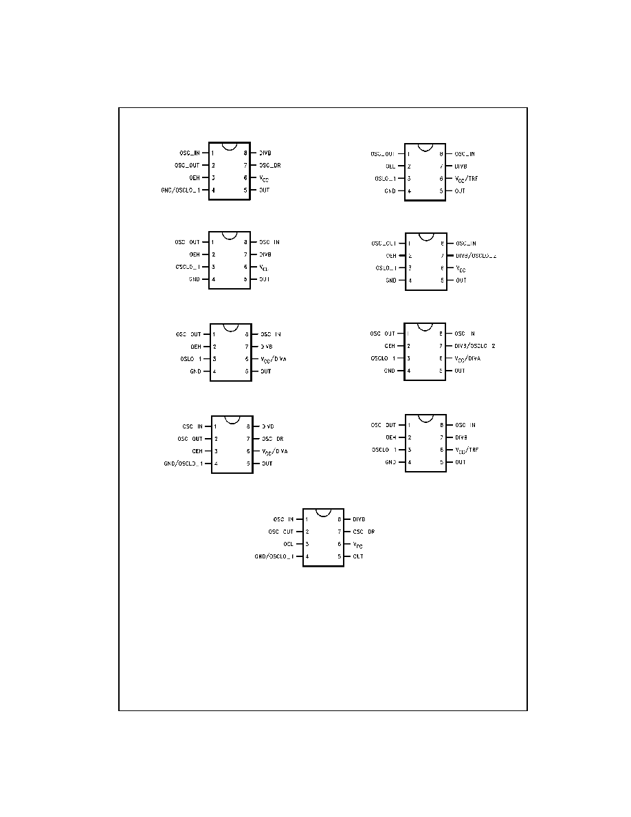
Connection Diagrams
(A) 3311
(B)3312
(C) 3313
(D) 3314
(E) 3315
(F) 3316
(G) 3317
(H) 3318
(I) 3319
3
www.fairchildsemi.com
CGS331
1
·
CGS3312 · C
G
S3313 · C
G
S3314
· C
G
S3315
· C
G
S3316
· CG
S331
7
· CG
S331
8
· CG
S331
9
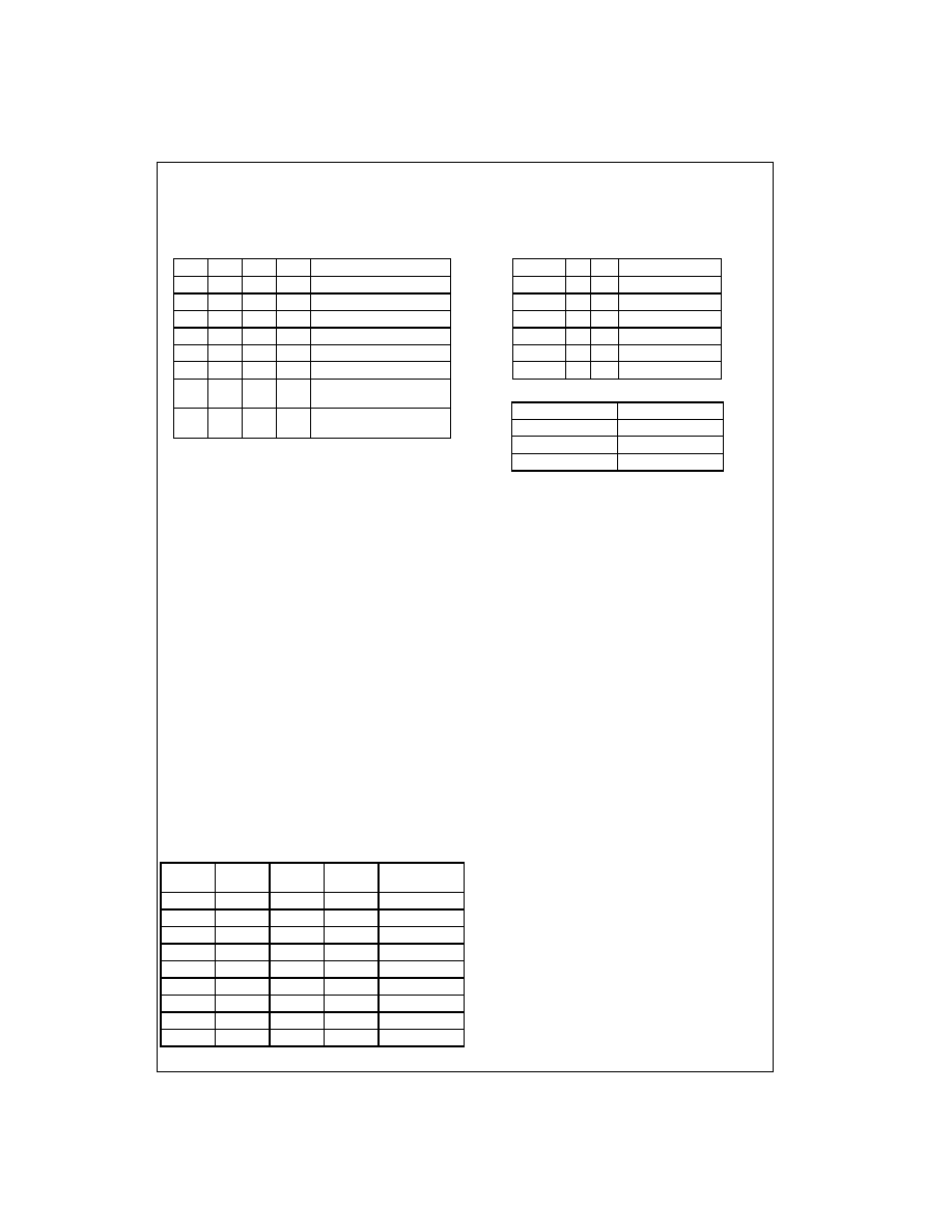
Truth Tables
Division Selection
Note: Actual value of the floating OSC_DR and DIVB input is V
CC/2
Rise and Fall Time Selection
Drive Selection
Note: Where "F" indicates floating the input.
Pin Descriptions
Functional Table
Summary of Device Options
Each drive has one output with the choices of selecting frequency divide,
output enable, crystal drive and output rise and fall time. Crystal drive
options are:
L
=
LOW Drive
M
=
MEDIUM Drive
H
=
HIGH Drive
DIVB DIVA OEL
OEH
Divider Output
F
0/F
X
X
Divide-by 1
1
0/F
0
1
Divide-by 2
0
0/F
0
1
Divide-by 4
F
1
0
1
Divide-by 8
1
1
0
1
Divide-by 16
0
1
0
1
Divide-by 32
X
X
1
X
Output Reset HIGH
at Re-enable
X
X
X
0
Output Reset HIGH
at Re-enable
OSC_DR DIV TRF Rise/Fall Time (ns)
F
N
0/F
2
F
N
1
less than 2
F
Y
0/F
4
F
Y
1
2
0,1
X
0/F
4
0,1
X
1
2
OSC_DR
Drive
0
Low
1
Medium
F
High
Note: Pin out varies for each device.
OSC_IN
Input to Oscillator Inverter. The output of the
crystal would be connected here.
OEL
Active LOW 3-STATE enable pin. This pin pulls
to a low value when left floating and 3-STATE
the output when forced HIGH. This pin has TTL
compatible input levels.
OSC_OUT Resistive Buffered Output of the Oscillator
Inverter
TRF
Rise and Fall time override pin. Available only
for die form.
OSC_DR
3 Level input pin that selects Oscillator Drive
Level
OUT
This pin is the main clock output on the device.
DIVA
Input used to select Binary Divide-by Option.
This pin has CMOS compatible input levels.
OSCLO_1
The Oscillator LOW pin is the ground for the
Oscillator.
OEH
Active HIGH 3-STATE enable pin. This pin pulls
to a high value when left floating and 3-STATEs
the output when forced low. This pin has TTL
compatible input levels.
OSCLO_2
This pin is the same signal as OSCLO_1. It has
been provided as an alternate connection for
OSCLO_1 for hybrid assemblies.
V
CC
The power pin for the chip.
GND
The ground pin for all sections of the circuitry
except the oscillator and oscillator related
circuitry.
Device
Divide
Enable
Drive
Output Rise/
Fall Time (ns)
3311
1, 2, 4
OEH
L, M, H
2, 4
3312
1, 2, 4
OEH
H
2, 4
3313
8, 16, 32
OEH
H
4
3314
8, 16, 32
OEH
L, M, H
4
3315
1, 2, 4
OEL
H
1, 2
3316
4
OEH
H
4
3317
32
OEH
H
4
3318
1, 2, 4
OEH
H
1, 2
3319
1, 2, 4
OEL
L, M, H
2, 4
www.fairchildsemi.com
4
CGS331
1
·
CGS3312 ·
CGS3313 ·
CGS3314 ·
CGS3315 · C
G
S3316 · C
G
S3317
· C
G
S3318
· C
G
S3319
Block Diagrams
Note: Pin numbers vary for each device
Oscillator Stage
Output Stage
5
www.fairchildsemi.com
CGS331
1
·
CGS3312 · C
G
S3313 · C
G
S3314
· C
G
S3315
· C
G
S3316
· CG
S331
7
· CG
S331
8
· CG
S331
9
Absolute Maximum Ratings
(Note 1)
Recommended Operating
Conditions
Note 1: The Absolute Maximum Ratings are those values beyond which
the safety of the device cannot be guaranteed. The device should not be
operated at these limits. The parametric values defined in the DC and AC
Electrical Characteristics tables are not guaranteed at the absolute maxi-
mum ratings. The Recommended Operating Conditions will define the con-
ditions for actual device operation.
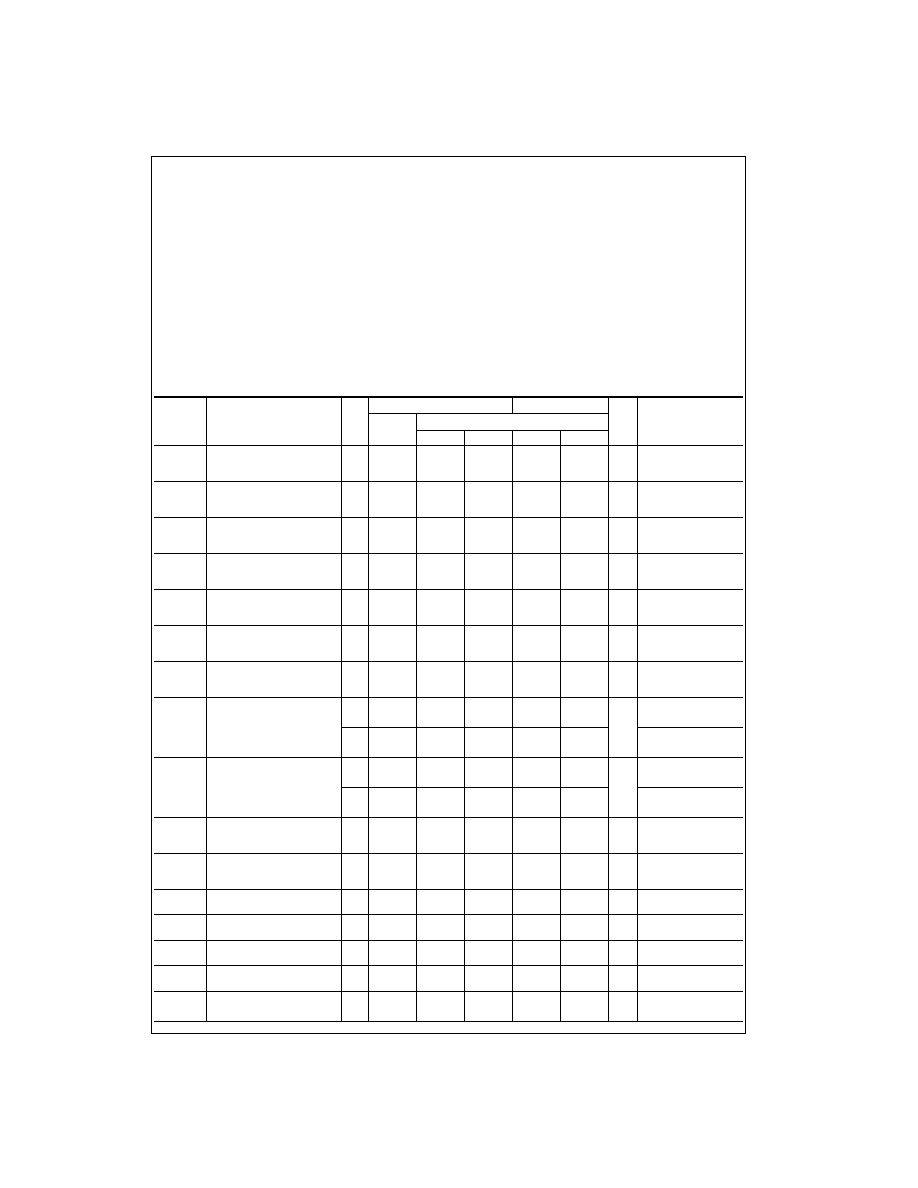
DC Electrical Characteristics
Supply Voltage (V
CC
)
-
0.5V to 7.0V
DC Input Voltage Diode Current (I
IK
)
±
9 mA
DC Input Voltage (V
I
)
-
0.5V to 7.0V
DC Output Diode Current (I
OK
)
±
20 mA
DC Output Voltage (V
O
)
-0.5V to V
CC
+
0.5V
DC Output Source
or Sink Current (I
O
)
±
70 mA
Storage Temperature (T
STG
)
-
55
°
C to 150
°
C
Junction Temperature (T
J
)
SOIC
140
°
C/W
Supply Voltage (V
CC
)
4.5V to 5.5V
Input Voltage (V
I
)
0V to 5.5V
Output Voltage (V
O
)
0V to V
CC
V
Operating Temperature (T
A
)
-
40
°
to
+
85
°
C
Symbol
Parameter
T
A
=
+
25
°
C
T
A
=
-
40
°
C to
+
85
°
C
Units Conditions
V
CC
Typ
Guaranteed Limits
(V)
Min
Max
Min
Max
V
IHTTL
Minimum HIGH Level
Input Voltage,
TTL Level Inputs (OEH, OEL)
4.5
2.0
2.0
V
5.5
2.0
2.0
V
ILTTL
Maximum LOW Level
Input Voltage, TTL Level
Inputs (OEH, OEL)
4.5
0.8
0.8
V
5.5
0.8
0.8
V
IHCMOS
Minimum HIGH Level
Input Voltage. CMOS
Level Inputs (DIVA)
4.5
3.15
3.15
V
5.5
3.85
3.85
V
ILCMOS
Maximum LOW Level
Input voltage. CMOS
Level Inputs (DIVA)
4.5
1.35
1.35
V
5.5
1.65
1.65
V
IN3L_H
Minimum Logic 1 Input
for Three Level Input
(DIVB, OSC_DR)
4.5
4.05
4.05
V
5.5
4.95
4.95
V
IN3L_1/2
Minimum Logic 1/2 Input
for Three Level Input
(DIVB, OSC_DR)
4.5
1.8
2.7
1.8
2.7
V
5.5
2.2
3.3
2.2
3.3
V
IN3L_L
Maximum Logic 0 Input
Level Three Level Input
(DIVB, OSC_DR)
4.5
0.45
0.45
V
5.5
0.45
0.45
V
OH
Minimum HIGH Level
Output Voltage
4.5
4.49
4.40
4.40
V
I
OUT
=
-
50
µ
A
5.5
5.49
5.40
5.40
4.5
3.86
3.76
I
OH
=
-
48 mA
5.5
4.86
4.76
V
IN
=
V
IH
or V
IH
V
OL
Minimum LOW Level
Output Voltage
4.5
0.001
0.1
0.1
V
I
OUT
=
50
µ
A
5.5
0.001
0.1
0.1
4.5
0.44
0.44
I
OL
=
+
48mA
5.5
0.44
0.44
V
IN
=
V
IL
or V
IH
I
IHRES
Input Current for Pins
DIVB, OSC_DR, and
DIVA (Input is Logic HIGH)
5.5
220
360
200
380
µ
A
V
IN
=
5.5V
I
ILRES
Input Current for Pins
DIVB, OSC_DR, and
DIVA (Input is Logic LOW)
5.5
-
220
-
360
-
200
-
380
µ
A
VIN
=
0.0V
I
IHENAB
Input Current for
Enable Pin OEL
5.5
90
160
85
175
µ
A
V
IN
=
5.5V
I
ILENAB
Input Current for
Enable Pin OEH
5.5
-
90
-
160
-
85
-
175
µ
A
V
IN
=
0.0V
I
IHOSC
Input Current for OSC_IN Pin
(Indicates Bias Resistance)
5.5
20
100
20
125
µ
A
V
IN
=
5.5V
I
ILOSC
Input Current for OSC_IN Pin
(Indicates Bias Resistance)
5.5
-
20
-
100
-
20
-
125
µ
A
V
IN
=
0.0V
I
OZH
Output Disabled Current
4.5
3.0
5.0
µ
A
V
OUT
=
V
CC
(Output HIGH)
5.5
3.0
5.0