 | –≠–ª–µ–∫—Ç—Ä–æ–Ω–Ω—ã–π –∫–æ–º–ø–æ–Ω–µ–Ω—Ç: XRD9814B | –°–∫–∞—á–∞—Ç—å:  PDF PDF  ZIP ZIP |

EXAR
Corporation, 48720 Kato Road, Fremont, CA 94538
∑
(510) 668-7000
∑
FAX (510) 668-7017
∑
www.exar.com
Rev. 1.00
XRD9814B/XRD9816B
3-Channel 14/16-Bit Linear
CCD/CIS Sensor Signal Processors
November 2002-2
FEATURES
∑
14-Bit (XRD9814B) or 16-Bit (XRD9816B)
A/D Converter
∑
Triple-Channel, 2.5 MSPS Color Scan Mode
∑
Single-Channel, 6 MSPS Monochrome Scan
Mode
∑
Triple Correlated Double Sampler
∑
Triple 10-Bit Programmable Gain Amplifier
∑
Triple 10-Bit Offset Compensation DAC
∑
Fully Differential or Single-Ended Inputs
∑
CDS or S/H Mode
∑
Inverting or Non-Inverting Mode
∑
Internal Voltage Reference
∑
Serial Control: On Data Bus or Separate Pins
∑
Improved PGA Performance
APPLICATIONS
∑
48-Bit Color Scanners (XRD9816B)
∑
42-Bit Color Scanners (XRD9814B)
∑
CCD or CIS Color Imagers
∑
Gray Scale Scanners
∑
Film Scanners
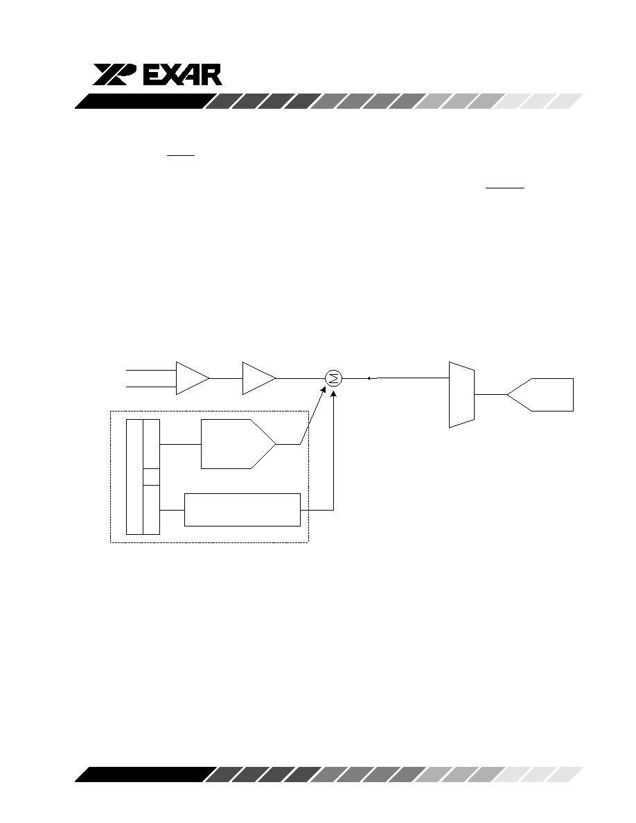
GENERAL DESCRIPTION
The XRD9814B/9816B is a fully integrated, high-per-
formance analog signal processor/digitizer specifi-
cally designed for use in 3-channel linear Charge
Coupled Device (CCD) and Contact Image Sensitive
(CIS) imaging applications.
Each channel of the XRD9814B/9816B includes a
Correlated Double Sampler (CDS), Programmable
Gain Amplifier (PGA) and channel offset adjustment.
After gain and offset adjustment, the analog inputs are
sequentially sampled and digitized by an accurate 14/
16-bit A/D converter. The analog front-end can be
configured for inverting/non-inverting input, CDS or
sample-hold (S/H) mode, or AC/DC coupling,
making the XRD9814B/9816B suitable for use in CCD,
CIS and other data acquisition applications.
∑
14-Bit or 8-Bit (Nibble) Parallel Data Output
(XRD9814B)
∑
16-Bit or 8-Bit (Nibble) Parallel Data Output
(XRD9816B)
∑
5V Operation and 3V I/O Compatibility
∑
Low Power CMOS: 500mW @ 5V
The CDS mode of operation supports both line and
pixel-clamp modes and can be used to achieve signifi-
cant reduction in system 1/f noise and CCD reset
clock feed-through. In S/H mode the internal DC-
restore voltage clamp can be enabled or disabled to
support AC-coupled or DC inputs. Sampling mode,
10-bit PGA gain (1024 linear steps), 8-bit fine offset
adjustment (256 linear steps), 2-bit gross offset adjust-
ment and input signal polarity are all programmable
through a serial interface. PGA gain range is 1 to 10,
and channel offset range is -300mV to 300mV for fine
adjustment and additional -400mV to +200mV for
gross offset adjustment. The A/D Full-Scale Range
(FSR) is programmable to 2V or 3V.
ORDERING INFORMATION
Part No.
Package Type
Temperature Range
XRD9814BCV
48-Lead TQFP
0∞C to +70∞C
XRD9816BCV
48-Lead TQFP
0∞C to +70∞C

XRD9814B/9816B
2
Rev. 1.00
RED(+)
RED(-)
INTERNAL TIMING CONTROL
REGISTER
REGISTER
REGISTER
REGISTER
PGA
REGISTER
REGISTER
VCLAMP
(Internal)
GRN(+)
GRN(-)
BLU(+)
BLU(-)
CREF
3-1
MUX
I/O CONTROL AND
CONFIGURATION
REGISTERS
BSAMP
VSAMP
ADCCLK
LCLMP
INSEL
OUTSEL
SDI
SCLK
LOAD
OEB
DB<13:0>
14/16
14/16-BIT A/D
REFIN
VREF+
VREF-
CAPN
CAPP
VREF
1.24V
DGND
DVDD
AVDD1
AVDD2
AVDD3
SGND
10-BIT
10-BIT
10-BIT
O
U
T
P
U
T
P
O
R
T
TEST1
TEST2
DB<15:0>
or
AGND1
AGND2
PGA
PROGRAMMABLE
BUFFERED
CDS or S/H
PROGRAMMABLE
BUFFERED
CDS or S/H
PROGRAMMABLE
BUFFERED
CDS or S/H
PGA
10-BIT
DAC
10-BIT
DAC
10-BIT
DAC
Figure 1. Block Diagram

XRD9814B/9816B
3
Rev. 1.00
XRD9814BCV
48
47
44
45
46
43
42
39
40
41
37
38
13
14
17
16
15
18
19
22
21
20
24
23
12
11
10
9
8
7
6
5
4
3
2
1
33
34
35
36
29
30
31
32
25
26
27
28
D
G
N
D
D
V
D
D
D
B
1
2
D
B
1
3
S
C
L
K
S
D
I
INSEL
O
U
T
S
E
L
L
O
A
D
O
E
B
VSAMP
ADCCLK
LCLMP
BSAMP
SGND
CAPN
AVDD1
AGND1
TEST2
CAPP
CREF
D
B
9
DB8
D
B
1
1
D
B
1
0
DB5
DB4
DB7
DB6
DB1
DB0
DB3
DB2
R
E
D
(
+
)
R
E
D
(
-
)
A
V
D
D
2
A
G
N
D
2
B
L
U
(
+
)
B
L
U
(
-
)
G
R
N
(
+
)
G
R
N
(
-
)
N
/
C
T
E
S
T
1
N
/
C
N
/
C
N/C
N/C
AVDD3
Note:
Pins 17,20 and 23 should be connected to AGND2 to improve noise immunity
PIN CONFIGURATION
PIN DESCRIPTION - XRD9814B
Pin No.
Name
Description
1
DB8
Data Output Bit 8
2
DB7
Data Output Bit 7
3
DB6
Data Output Bit 6
4
DB5
Data Output Bit 5
5
DB4
Data Output Bit 4
6
DB3
Data Output Bit 3
7
DB2
Data Output Bit 2
8
DB1
Data Output Bit 1
9
DB0
Data Output Bit 0
10
N/C
No Connect
11
N/C
No Connect
12
AV
DD3
Analog Power Supply
13
AV
DD2
Analog Power Supply
14
AGND2
Analog Ground (Substrate)
15
RED(+)
Red Positive Analog Input

XRD9814B/9816B
4
Rev. 1.00
Note 1: INSEL=0 --> SCLK, SDI, and LOAD pins are active for serial programming; INSEL=1 --> SCLK and SDI pins
are inactive, and the serial programming is done through I/O pins DB12 and DB13 as described in Notes 3~4 with
LOAD tri-stating DB12 and DB13.
Note 2: OUTSEL=0 --> 14-bit parallel output mode select; OUTSEL=1 --> 8-bit nibble output mode select.
Note 3: For INSEL=1, DB12 becomes the SCLK input during serial programming.
Note 4: For INSEL=1, DB13 becomes the SDI input during serial programming.
Note 5: Pins 17, 20 and 23 may be connected to AGND2 to improve noise immunity.
PIN DESCRIPTION - XRD9814B (CONT'D)
Pin No.
Name
Description
16
RED(-)
Red Negative Analog Input
17
N/C
No Connect, (Note 5)
18
GRN(+)
Green Positive Analog Input
19
GRN(-)
Green Negative Analog Input
20
N/C
No Connect, (Note 5)
21
BLU(+)
Blue Positive Analog Input
22
BLU(-)
Blue Negative Analog Input
23
N/C
No Connect, (Note 5)
24
TEST1
Internal Use Only
25
TEST2
Internal Use Only
26
CREF
Decoupling Cap for CDS Reference
27
CAPP
Decoupling Cap for Positive Reference
28
CAPN
Decoupling Cap for Negative Reference
29
SGND
Substrate Gnd
30
AGND1
Analog Ground (Substrate)
31
AV
DD1
Analog Power Supply
32
LCLMP
Line Clamp Enable
33
VSAMP
Video Level Sampling Clock
34
BSAMP
Black Level Sampling Clock
35
ADCCLK
A/D Converter Clock
36
INSEL
Input Mode Select (Note 1)
37
OUTSEL
Output Mode Select (Note 2)
38
OEB
Data Output Enable
39
LOAD
Register Write Enable (Note 5)
40
SDI
Serial Data Input (Note 4)
41
SCLK
Serial Shift Clock (Note 3)
42
DGND
Ground (Output Drivers and Internal Decode Logic)
43
DV
DD
Digital Power Supply (Output Drivers and Internal Decode Logic)
44
DB13
Data I/O Bit 13 (Note 4)
45
DB12
Data I/O Bit 12 (Note 3)
46
DB11
Data Output Bit 11
47
DB10
Data Output Bit 10
48
DB9
Data Output Bit 9

XRD9814B/9816B
5
Rev. 1.00
XRD9816BCV
48
47
44
45
46
43
42
39
40
41
37
38
13
14
17
16
15
18
19
22
21
20
24
23
12
11
10
9
8
7
6
5
4
3
2
1
33
34
35
36
29
30
31
32
25
26
27
28
D
G
N
D
D
V
D
D
D
B
1
4
D
B
1
5
S
C
L
K
S
D
I
INSEL
O
U
T
S
E
L
L
O
A
D
O
E
B
VSAMP
ADCCLK
LCLMP
BSAMP
SGND
CAPN
AVDD1
AGND1
TEST2
CAPP
CREF
D
B
1
1
DB10
D
B
1
3
D
B
1
2
DB7
DB6
DB9
DB8
DB3
DB2
DB5
DB4
R
E
D
(
+
)
R
E
D
(
-
)
A
V
D
D
2
A
G
N
D
2
B
L
U
(
+
)
B
L
U
(
-
)
G
R
N
(
+
)
G
R
N
(
-
)
N
/
C
T
E
S
T
1
N
/
C
N
/
C
DB1
DB0
AVDD3
Note:
Pins 17,20 and 23 should be connected to AGND2 to improve noise immunity
PIN CONFIGURATION
Pin No.
Name
Description
1
DB10
Data Output Bit 10
2
DB9
Data Output Bit9
3
DB8
Data Output Bit 8
4
DB7
Data Output Bit 7
5
DB6
Data Output Bit 6
6
DB5
Data Output Bit 5
7
DB4
Data Output Bit 4
8
DB3
Data Output Bit 3
9
DB2
Data Output Bit 2
10
DB1
Data Output Bit 1
11
DB0
Data Output Bit 0
12
AV
DD3
Analog Power Supply
13
AV
DD2
Analog Power Supply
14
AGND2
Analog Ground (Substrate)
15
RED(+)
Red Positive Analog Input

XRD9814B/9816B
6
Rev. 1.00
Pin Configuration - XRD9816B
Pin No.
Name
Description
16
RED(-)
Red Negative Analog Input
17
N/C
No Connect, (Note 5)
18
GRN(+)
Green Positive Analog Input
19
GRN(-)
Green Negative Analog Input
20
N/C
No Connect, (Note 5)
21
BLU(+)
Blue Positive Analog Input
22
BLU(-)
Blue Negative Analog Input
23
N/C
No Connect, (Note 5)
24
TEST1
Internal Use Only
25
TEST2
Internal Use Only
26
CREF
Decoupling Cap for CDS Reference
27
CAPP
Decoupling Cap for Positive Reference
28
CAPN
Decoupling Cap for Negative Reference
29
SGND
Substrate Gnd
30
AGND1
Analog Ground (Substrate)
31
AV
DD1
Analog Power Supply
32
LCLMP
Line Clamp Enable
33
VSAMP
Video Level Sampling Clock
34
BSAMP
Black Level Sampling Clock
35
ADCCLK
A/D Converter Clock
36
INSEL
Input Mode Select (Note 1)
37
OUTSEL
Output Mode Select (Note 2)
38
OEB
Data Output Enable
39
LOAD
Register Write Enable (Note 5)
40
SDI
Serial Data Input (Note 4)
41
SCLK
Serial Shift Clock (Note 3)
42
DGND
Ground (Output Drivers and Internal Decode Logic)
43
DV
DD
Digital Power Supply (Output Drivers and Internal Decode Logic)
44
DB15
Data I/O Bit 15 (Note 4)
46
DB13
Data Output Bit 13
45
DB14
Data I/O Bit 14 (Note 3)
47
DB12
Data Output Bit 12
48
DB11
Data Output Bit 11
Note 1: INSEL=0 --> SCLK, SDI, and LOAD pins are active for serial programming; INSEL=1 --> SCLK and SDI
pins are inactive, and the serial programming is done through I/O pins DB14 and DB15 as described in
Notes 3~4 with LOAD tri-stating DB14 and DB15.
Note 2: OUTSEL=0 --> 16-bit parallel output mode select; OUTSEL=1 --> 8-bit nibble output mode select.
Note 3: For INSEL=1, DB14 becomes the SCLK input during serial programming.
Note 4: For INSEL=1, DB15 becomes the SDI input during serial programming.
Note 5: Pins 17, 20 and 23 may be connected to AGND2 to improve noise immunity.

XRD9814B/9816B
7
Rev. 1.00
ELECTRICAL CHARACTERISTICS
AV
DD
=DV
DD
=5.0V, ADCCLK=6MHz, Input Range = 2V, Ta=25
o
C unless otherwise specified
Parameter
Symbol
Min
Typ
Max
Unit
Conditions
A/D CONVERTER
Resolution
R
14
BITS
XRD9814B
Resolution
R
16
BITS
XRD9816B
Maximum Conversion Rate
Fc
6
8
MSPS
Differential Non-Linearity
DNL
+/-0.8
LSB
XRD9814B
Differential Non-Linearity
DNL
-0.95/+1.2
LSB
XRD9816B
Monotonicity
M
Yes
XRD9814B
Monotonicity
M
Yes
XRD9816B
Input Referred Offset
ZSE
40
mV
Offset Drift
ZSD
15
uV/
o
C
Input Referred Gain Error
FSE
+/- 2
% FS
Gain Error Drift
FSD
0.003
% FS
o
C
Input Voltage Range
2V Full-Scale Range
IVR
0
2.0
V
PB5=0, Config Reg #1
3V Full-Scale Range
IVR
0
3.0
V
PB5=1, Config Reg #1
CDS - S/H SPECIFICATIONS
Input Voltage Range
Input Buffer Disabled
INVSR
AGND
AVDD
V
Pixel Clamp,
(Note 1)
PB1=0, Config Reg #1
Input Buffer Enabled
INVSRB
0.5
AVDD-1
V
Line Clamp,
PB1=1, Config Reg #1
Input Bias Current
Input Buffer Disabled
IB
25
uA
Gain=1,
(Note 2)
PB1=0, Config Reg #1
Input Buffer Enabled
IBB
25
nA
T
A
=70
o
C,
PB1=1, Config Reg #1
Input Switch On -Resistance
Ron
150
250
Clamp Enabled
Input Switch Off -Resistance
Roff
100
1000
M
Clamp Disabled
Internal Voltage Clamp
CCD Input (Inverting)
Vclamp
4.0
4.2
4.4
V
PB2=0, Config Reg #1
S/H Input (Non-Inverting)
Vclamp
0.6
0.8
1.0
V
PB2=1, Config Reg #1
Note 1: ADC digitizing range = (A/D Full-Scale Range/PGA Gain)
Note 2: Due to switch capacitor input.

XRD9814B/9816B
8
Rev. 1.00
ELECTRICAL CHARACTERISTICS (CONT'D)
AVDD=DVDD=5.0V, ADCCLK=6MHz, Ta=25C unless otherwise specified
Parameter
Symbol
Min
Typ
Max
Unit
Conditions
OFFSET SPECIFICATIONS
Fine Offset Adjustment Min
OFR
-270
-300
-330
mV
Fine Offset Adjustment Max
OFR
+270
+300
+330
mV
Fine Offset Adjustment Step
OFRES
2.34
mV
8-Bit, 256 Settings
Fine Offset Adjustment
OFRL
+/-1.5%
Linearity
Gross Offset Adjustment Min
OFGR
-360
-400
-440
mV
Gross Offset Adjustment Max
OFGR
+360
+200
+440
mV
Gross Offset Adjustment Step OFGRES
+200
mV
2-Bit, 4 Settings
PGA SPECIFICATIONS
Gain Range Min
(Absolute Value)
GRAN
1.0
1.10
1.20
V/V
-1 for PB2=0,
+1 for PB2=1, Config Reg #1
Gain Range Max
(Absolute Value)
GRAN
8.5
9.5
10.5
V/V
-10 for PB2=0,
+10 for PB2=1,
Config Reg#1
Gain Resolution
GRES
0.0083
V/V
10-Bit 1024 Steps
Gain DNL
+/-2.0
LSB
By design
SYSTEM SPECIFICATIONS (Includes CDS, PGA and A/D)
Differential Non-Linearity
DNL
-0.9
+/-0.8
+1.5
LSB
XRD9814B, PGA Gain = 1
Differential Non-Linearity
DNL
-0.95
-0.95/+1.2
+2.0
LSB
XRD9816B, PGA Gain = 1
Integral Non-Linearity
INL
+/-10.0
LSB
XRD9814B, PGA Gain = 1
Input Referred Noise
PGA Gain = -1.63
IRN
min
+3.4
LSB
XRD9814B, 1-Channel CIS
Mode, 6MSPS, Low Gain
PGA Gain = -5.0
IRN
max
+1.1
LSB
XRD9814B, 1-Channel CIS
Mode, 6MSPS, Low Gain
System Offset
PGA Gain= -1
IRO
min
+70
mV
XRD9814B/9816B, 3-Channel
Mode, 6MSPS
PGA Gain= -10
IRO
max
+70
mV
XRD9814B/9816B, 3-Channel
Mode, 6MSPS

XRD9814B/9816B
9
Rev. 1.00
ELECTRICAL CHARACTERISTICS (CONT'D)
AVDD=DVDD=5.0V, ADCCLK=6MHz, Ta=25C unless otherwise specified
Parameter
Symbol
Min
Typ
Max
Unit
Conditions
TIMING SPECIFICATIONS
ADCCLK Pulse Width
taclk
66.5
ns
BSAMP falling edge delay from
tbfcr
10
ns
rising ADCCLK
BSAMP falling edge to VSAMP
tbvf
70
ns
falling edge.
ADCCLK Period (1 Ch. Mode)
tcp1
166
ns
ADCCLK Period (3 Ch. Mode)
tcp3
133
ns
1-Channel Conversion Period
tcr1
166
ns
3-Channel Conversion Period
tcr3
400
ns
BSAMP Pulse Width
tpwb
30
ns
VSAMP Pulse Width
tpwv
30
ns
VSAMP falling edge to BSAMP
tvbf
70
ns
falling edge.
VSAMP falling edge delay from
tvfcr
30
ns
All modes except 1-Channel
rising ADCCLK.
S/H
VSAMP falling edge delay
tvfcr
70
ns
1-Channel S/H, Config
from rising ADCCLK
REG #1, PB2=1, PB7=1
PGA Settling Time
tstl
70
ns
Aperture Delay
tap
5
ns
VSAMP TIMING OPTION #1
VSAMP rising edge delay from
tvrcf
15
ns
tvrcr is not required, Config
falling ADCCLK (Note 1)
REG #1, PB0=0
VSAMP TIMING OPTION #2
VSAMP rising edge delay from
tvrcr
15
ns
tvrcf is not required, Config
rising ADCCLK (Note 1)
REG # 1, PB0=1
WRITE SPECIFICATIONS
Data Setup Time
tds
15
ns
Data Hold Time
tdh
15
ns
Load Setup Time
tlcs
15
ns
Load Hold Time
tlch
15
ns
Load Pulse Width
tplw
25
ns
Note 1:
VSAMP Timing Option #2 allows additional timing flexibility by allowing the rising edge of VSAMP to occur
approximately one-half ADCCLK period earlier than Option #1. Option #2 is only available in 3-Channel
Operation (PB4=0, PB3=0, Configuration Register #1).

XRD9814B/9816B
10
Rev. 1.00
ELECTRICAL CHARACTERISTICS (CONT'D)
AVDD=DVDD=5.0V, ADCCLK=6MHz, Ta=25C unless otherwise specified
Parameter
Symbol
Min
Typ
Max
Unit
Conditions
DATA READBACK SPECIFICATIONS
Address Access Time
taa (1)
15
ns
Output Enable Access Time
taoe (1)
15
ns
ADC DIGITAL OUTPUT SPECIFICATIONS
Output Delay
tod
20
ns
Tri-State to Data Valid
tlz
8
ns
Output Enable High to Tri-State
thz
8
ns
Latency RGB inputs
lat
7
ADCCLK
DIGITAL INPUTS
Input High Logic Level
V
IH
80
% DV
DD
DV
DD
=3-5V
Input Low Logic Level
V
IL
20
% DV
DD
DV
DD
=3-5V
High Level Input Current
I
IH
5
uA
Low Level Input Current
I
IL
5
uA
Input Capacitance
C
IN
10
pF
DIGITAL OUTPUTS (DV
DD
=5V)
Output High Voltage
V
OH
4.2
V
IL=2ma
Output Low Voltage
V
OL
0.4
V
IL=-2ma
Output Capacitance
C
OUT
10
pF
DIGITAL OUTPUTS (DV
DD
=3.3V)
Output High Voltage
V
OH
2.8
V
IL=2ma
Output Low Voltage
V
OL
0.3
V
IL=-2ma
Output Capacitance
C
OUT
10
pF
POWER SUPPLY
Analog Power Supply
AV
DD
4.5
5.0
5.5
V
Digital Power Supply
DV
DD
3.0
5.0
5.5
V
Analog Supply Current
IDDA
110
mA
3CH CDS Mode
Digital Supply Current
IDDD
2
mA
Digital Output CLoad=30pF,
all pins.
Stand-By Mode Power
PDoff
65
80
mW
Note 1: Start of valid data depends on which timing becomes effective last, taoe or taa.

XRD9814B/9816B
11
Rev. 1.00
Function
A2
A1
A0
PB9-PB0
Configuration Reg #1
0
0
0
See Configuration Register #1
Configuration Reg #2
0
0
1
See Configuration Register #2
Red Gain
0
1
0
10-Bit Gain
Green Gain
0
1
1
10-Bit Gain
Blue Gain
1
0
0
10-Bit Gain
Red Offset
1
0
1
2-Bit Gross Offset Adjustment: 8-Bit Fine Offset Adjustment
Green Offset
1
1
0
2-Bit Gross Offset Adjustment: 8-Bit Fine Offset Adjustment
Blue Offset
1
1
1
2-Bit Gross Offset Adjustment: 8-Bit Fine Offset Adjustment
Table 1. XRD9814B/9816B Register Overview
A2
A1
A0
Bit
PB9-PB0 Bit Definition
Address
Assignment
0
0
0
PB9 Single Channel
0
Unused channels are powered down to 0
Power Save Mode
save power (single channel mode only)
1
Unused channels are powered up
PB8 Digital Reset
0
No Reset
1
Resets all registers to the default configuration
PB7 PB6
Clamp Mode
00 CDS pixel
01 CDS line clamp
10 No clamp
11 S/H line clamp
PB5 A/D Full Scale Range
0
2Vpp Full Scale
1
3Vpp Full Scale (recommended for better performance)
PB4 PB3
00 RGB 3 channel color mode
Color Select
01 Red single channel mode
10 Green single channel mode
11 Blue single channel mode
PB2
Input Signal Polarity
0
Inverted for CCD or negative going signals
1
Non-inverted for CIS or positive going signals
PB1
Input Buffer Enable
0
No buffer (DC coupled or AC coupled inputs
with pixel clamp mode
1
Buffer enabled (AC Coupled inputs for line clamp or no
clamp mode
PB0
VSAMP Timing
0
Timing option #1 (see Figure 3, 4, 7 & 8 for details)
1
Timing option #2 (see Figure 3, 4, 7 & 8 for details)
Table 2. Configuration Register #1 Definition (Default Configuration is 000H)

XRD9814B/9816B
12
Rev. 1.00
A2
A1
A0
Bit
PB9-PB0 Bit Definition
Address
Assignment
0
0
1
PB9
0
Normal
This register should be set to zero for normal operation
Not Used
1
Do Not Use
PB8
0
Normal
This register should be set to zero for normal operation
Not Used
1
Do Not Use
PB7
0
Normal This register should be set to zero for normal operation
Not Used
1
Do Not Use
PB6
0
Normal
This register should be set to zero for normal operation
Not Used
1
Do Not Use
PB5
0
Normal
This register should be set to zero for normal operation
Not Used
1
Do Not Use
PB4 PB3
00
AV
DD
-0.8V (4.2V for AVDD = 5V) (See Figures 11 & 12 for VClamp
Settings)
CDS Clamp Voltage 01
AV
DD
-1.3V (3.7V for AVDD = 5V)
(Black Level)
10
AV
DD
-1.8V (3.2V for AVDD = 5V)
11
AV
DD
-2.3V (2.7V for AVDD = 5V)
PB2
0
Normal
This register should be set to zero for normal operation
Not Used
1
Do Not Use
PB1
0
All circuits active
Stand-By Mode
1
Low power mode (75mW, requires 5uS back to normal operation)
PB0
0
A/D digital outputs
Read Back Mode
1
Read back mode (A2:A1:A0 select register data)
Table 3. Configuration Register #2 Definition (Default Configuration is 000H)

XRD9814B/9816B
13
Rev. 1.00
A2
A1
A0
Function
PB9
PB8
PB7
PB6
PB5
PB4
PB3
PB2
PB1
PB0
0
1
0
Red Gain
MSB
LSB
0
1
1
Green Gain
MSB
LSB
1
0
0
Blue Gain
MSB
LSB
1
0
1
Red Offset
00
0V
MSB
LSB
PB9-PB8 gross adj
01
+200mV
PB7-PB0 fine adj
10
-200mV
11
-400mV
1
1
0
Green Offset
00
0V
MSB
LSB
PB9-PB8 gross adj
01
+200mV
PB7-PB0 fine adj
10
-200mV
11
-400mV
1
1
1
Blue Offset
00
0V
MSB
LSB
PB9-PB8 gross adj
01
+200mV
PB7-PB0 fine adj
10
-200mV
11
-400mV
Table 4. Gain and Offset Registers (Default Configuration is 000H)

XRD9814B/9816B
14
Rev. 1.00
GENERAL DESCRIPTION
The XRD9814B/9816B contains all of the circuitry
required to create a complete 3-channel signal proces-
sor /digitizer for use in CCD/CIS imaging systems.
Each channel includes a correlated double sampler
(CDS), programmable gain amplifier (PGA) and chan-
nel offset adjustment. The input stage can also be
configured for use with inverting/non-inverting, AC or
DC coupled signals. In order to maximize flexibility, the
specific operating mode is programmable through two
configuration registers. In addition, the gain and offset
of each channel can be independently programmed
through separate gain and offset registers. Configura-
tion register data is loaded serially through a 3-pin
serial interface. Specific details for register writes are
detailed below. After signal conditioning the three PGA
outputs are digitized by a 14-bit/16-bit A/D converter.
Writing Registers Data
The XRD9814B/9816B utilizes eight 10-Bit registers to
store configuration, gain and offset information. Regis-
ter data is written through the 3-pin serial interface
consisting of SDI (serial data input), SCLK (serial shift
clock) and LOAD (positive edge write enable). A write
consists of pulling LOAD low, shifting in 3 bits of
address (MSB first) and 10 bits of data (MSB first).
Data is written on the rising edge of SCLK and the last
13 bits are latched. The timing for writing to registers
is shown in Figure 17 and 18.
When INSEL=0, SCLK, SDI, and LOAD pins are active
for serial programming.
When INSEL=1, SCLK and SDI pins are inactive, and
the serial programming is done through I/O pins DB12/
DB14 and DB13/DB15 while LOAD pin is low.
Configuration Register #1
The bit assignment and definition for this register is
detailed in the Configuration Register #1 Definition
Table (Table 2). The primary purpose of this register is
to configure the analog input blocks for CCD or S/H
operation.
Clamp Mode
The clamp mode setting determines the conditions
when the internal clamp is enabled (see Table 5). The
pixel and CCD line-clamp modes are used to DC-
restore AC coupled CCD input signals to the PGA
common-mode input voltage while using correlated
double sampling. S/H line mode should be used to DC-
restore AC coupled inputs which do not utilize corre-
lated double sampling and have only one control input
(VSAMP). No-clamp mode should be used for DC
coupled S/H inputs.
Pixel Mode (CCD with CDS)
The input clamp is active each pixel period with a
pulse-width determined by the Black- level Sampling
Input (BSAMP). The position of BSAMP can be opti-
mized to eliminate the effects of the CCD reset pulse.
Since the input capacitor is recharged to the clamp
voltage on each pixel, common-mode droop errors are
eliminated.
CCD Line Mode (CCD with CDS)
The input clamp is enabled only at the beginning of the
line by gating BSAMP with LCLMP. Gating with
LCLMP maintains the ability to position the clamp
pulse (BSAMP) away from the CCD reset for varying
LCLMP position and width. Since the input capacitor
is clamped only at the beginning of each line a larger
input capacitor is required to satisfy the common-mode
input requirements of the analog front-end. (See Cou-
pling Capacitor Requirements.) The input buffer should
be enabled in this mode (PB1=1, Register #1).
S/H Line Mode (S/H with AC Coupling)
The S/H Line mode clamp is used to DC-restore AC
coupled inputs which do not utilize CDS. VSAMP is
used to sample and hold the input signal and LCLMP
performs the clamp function. This differs from the CDS
line and pixel modes which use BSAMP to clamp to the
reference level and VSAMP to hold the video input. The
input buffer should be enabled in this mode (PB1=1,
Register #1).

XRD9814B/9816B
15
Rev. 1.00
Clamp
Mode
PB7
PB6
Clamp Enable
Pixel
0
0
BSAMP
CDS Line
0
1
No Clamp
1
0
Disabled
S/H Line
1
1
BSAMP LCLMP
LCLMP
Table 5. Clamp Enable Definition
Clamp
Enable
BSAMP
LCLMP
PB6
PB7
No-Clamp Mode (S/H with DC input)
Used for DC coupled inputs. AC coupled inputs must
be externally clamped to the proper common-mode
input voltage of the XRD9814B/9816B.
Note: Pixel clamp is the default clamp mode.
Figure 2. Clamp Enable Logic
A/D Full-Scale Range
This bit sets the Full-Scale Range (FSR) of the A/D
converter to 2V or 3V. Use the 3V FSR for lowest
noise performance.
Color Select
The color input corresponds to the signal input to be
digitized by the A/D converter. If set to RGB (default)
the A/D input is sequentially cycled through the red,
green and blue channels. The green channel is syn-
chronized on the rising edge of the first ADCCLK after
the falling edge of VSAMP. If set in single-channel mode,
the A/D multiplexer will not sequence and the A/D con-
verter input will be continually connected to the chan-
nel that is selected, RED, GRN or BLU.
Signal Polarity
This bit configures the analog inputs for positive or
negative transitioning inputs. This is required to pro-
vide the correct signal polarity to the A/D input and to
set the correct input clamp level. The default configu-
ration is set to inverting mode (CCD input).
Input Buffer Enable
This bit enables the input buffer to the PGA amplifier
and is required only for AC coupled inputs operating in
CDS line or S/H line clamp modes. Since this input
buffer reduces the input voltage range its use is not
recommended under DC or pixel-mode operation. The
input buffer is disabled in the default configuration.

XRD9814B/9816B
16
Rev. 1.00
VSAMP Timing
This allows the user to select one of two VSAMP timing
controls. Timing Option #2 allows the rising edge of
VSAMP to occur approximately one-half ADCCLK
earlier than Option #1. This does not affect internal
timing and is provided only to allow additional flexibility
in the external timing control. Timing Option #2 is
available only in the 3-channel mode of operation (See
timing diagrams Figure 3 and Figure 4).
Configuration Register #2
The bit assignment and definition for this register is
detailed in the Configuration Register #2 Definition
Table. A diagnostic read-back mode allows gain,
offset and configuration data to be output as the 8 or 10
MSBs on the digital output bus depending on the
selection of OUTSEL (see Reading Register Data
session for details). Additional bits are used to enable
a low-power stand-by state and manufacturing test
mode.
Digital Reset
Setting this bit to one resets all registers to all zeros.
Test Mode
This is a reserved bit for testing and must be set to 0
in all writes to Configuration Register #2.
Stand-By Mode
Setting this bit to one forces the circuit into a low-power
standby mode. Configuration, offset and gain registers
remain unchanged in stand-by mode. Pull OEB High
to set DB<15:0> to high impedance during stand-by
mode.
Read Back Mode
This is a special diagnostic mode which can aid in the
debugging of new system designs. Setting this bit to 1
allows all configuration, gain and offset register con-
tents to be output on the data output bus (explained
below).
Reading Register Data
In order to enter read-back mode, set configuration
register #2, PB0 to 1. Follow the write timing in Figures
17 and 18.
In order to read a specific register, shift in 3-bits of
register address data (MSB first), followed by 10
dummy data bits. In the case of reading back configu-
ration register #2, PB0 has to stay 1 and cannot be a
dummy.
In order to exit read-back mode perform a write to
configuration register 2, PB0=0.
(OUTSEL = 0) In read-back mode the A/D output is
bypassed and internal register data is output to the 10
most significant bits of the data output bus. The
remaining LSB bits should be ignored. Register data
will be valid after the load pin goes high.
(OUTSEL = 1) In nibble mode, the output bus is limited
to 8-bits. Therefore, in read-back mode, the 8 MSBs
are valid when ADCCLK is high, and the 2 LSBs are
valid when ADCCLK is low. Configuring and exiting the
read-back mode is done in the same manner of
OUTSEL = 0.
Important: The entire byte of register #2 is re-written when
exiting the readback mode. If any bits of configuration
register #2 were programmed prior to entering the read-
back mode, they must be re-programmed when exiting
read-back. See Figure 19 for read-back timing.
PGA Gain Settings
The gain for each color input is individually program-
mable from 1 to 10 in 1024 linear steps.
001 XXXXXXXXX1
010 XXXXXXXXXX
Cfig2
Red Gain
011 XXXXXXXXXX
Grn Gain
100 XXXXXXXXXX
Blu Gain
101 XXXXXXXXXX
Red Offset
110 XXXXXXXXXX
111 XXXXXXXXXX
001 XXXXXXXXXX
Cfig1
Blu Offset
Grn Offset
Address Data
Register
Read-Back Registers and Address
XRD9814B/9816B
17
Rev. 1.00
where Code represents the binary contents of the 10-
bit gain setting register.
Channel Offset Adjustment
The gross offset correction for each channel is
progammable from -400mV to +200mV. It is adjusted
by toggling PB9 and PB8 of Offset Registers (Table 4).
Theory of Operation
Code
1024
9 0 + 1
.
PGA Gain =
PB7=1 equals -1
PB7=0 equals +1
Code = (PB6:PB0) of the 10-bit offset register.
Block Diagram of the Fine and Gross Offset Adjustment DAC
CDS
PGA
10-Bit
Differential
Input
XRD9814B/16B
ADC
14-Bit
3:1
MUX
8
-
B
i
t
2
-
B
i
t
P
r
o
g
r
a
m
m
a
b
l
e
S
e
r
i
a
l
P
o
r
t
8-Bit Offset DAC
Fine Adjust
2-Bit Offset
Variable Capacitive Divider
Gross Adjust
Offset Block
Vout
The fine offset correction for each channel is program-
mable from -300mV to +300mV.
Fine Channel Offset =
(
)
PB
Code
7
128
300mV

XRD9814B/9816B
18
Rev. 1.00
(Correlated Double Sampling)
Correlated double sampling is a technique used to level
shift and acquire CCD output signals whose informa-
tion is equal to the difference between consecutive
reference (black) and signal (video) samples. The CDS
process consists of three steps:
1)
Sampling and holding the reference black level.
2)
Sampling the video level.
3)
Subtracting the two samples to extract the video
information.
Once the video information has been extracted it can
be processed further through amplification and/or off-
set adjustment. Since system noise is also stored and
subtracted during the CDS process, signals with band-
widths less than half the sampling frequency will be
substantially attenuated.
In order to reject higher frequency power supply noise
which is not attenuated near the sampling frequency
the XRD9814B/9816B utilizes a fully differential input
structure.
Since the CDS process uses AC coupled inputs the
coupling capacitor must be charged to the common-
mode range of the analog front-end. This can be
accomplished by clamping the coupling capacitor to
the internal clamp voltage when the CCD is at a
reference level. This clamp may occur during each
pixel (Pixel Clamp), or at the beginning of each line
(CDS Line Clamp). If CDS Line Clamp mode is used the
input buffer (configuration register #1, PB1) must be
enabled to eliminate the effects of input bias current.
If Pixel mode is selected the input buffer is not required
or recommended.
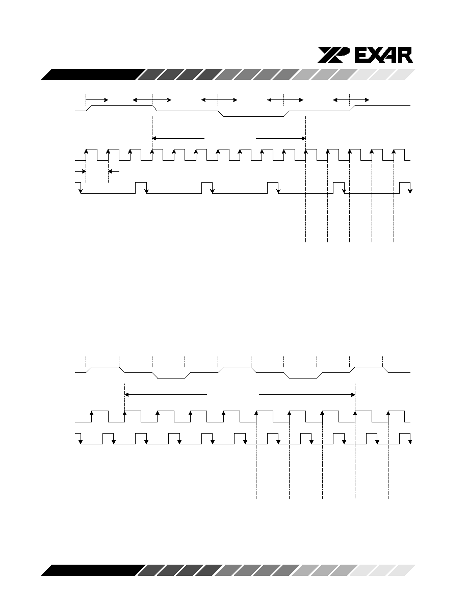
3-Channel CDS Mode
This mode allows simultaneous CDS of the red, green
and blue inputs . Black-level sampling occurs on each
pixel and is equal to the width of the BSAMP sampling
input. The black level is held on the falling edge of
BSAMP and the PGA will immediately begin to track
the signal input until the falling edge of VSAMP.
Two VSAMP timing modes are supported to allow
additional flexibility in the VSAMP pulse width (see
timing diagrams). At the end of the video sampling
phase the difference between the reference and video
levels is inverted, amplified and offset depending on
the contents of the PGA gain and offset registers. The
RGB channels are then sequentially converted by a
high speed A/D converter. A/D converter data appears
on the data output bus after 7 ADCCLK cycles. The
green channel is synchronized on the rising edge of the
first ADCCLK after the falling edge of VSAMP. The
power-up default mode is for CDS sampling a CCD
input (Pixel Clamp, Inverting Input, No Input Buffer).
1-Channel CDS Mode
The 1-Channel CDS mode allows high-speed acquisi-
tion and processing of a single channel. The timing,
clamp and buffer configurations are similar to the 3-
channel mode described previously. To select a single
channel input the color bits of configuration register 1
must be set to the appropriate value. The A/D input will
begin to track the selected color input on the next
positive edge of ADCCLK. If the configuration is
toggled from single color to 3-channel mode RGB
scanning will not occur until the circuit is
resynchronized on the falling edge of VSAMP.

XRD9814B/9816B
19
Rev. 1.00
3-Channel CIS/Sample and Hold Mode
The XRD9814B/9816B also supports operation for
Contact Image Sensor (CIS) and S/H applications. The
green channel is synchronized on the rising edge of the
first ADCCLK after the falling edge of VSAMP.
For DC coupled inputs the reference clamp and input
buffer should be disabled and input polarity should be
set to 1 (non-inverting). In this mode of operation the
BSAMP input is connected to DGND and input sam-
pling occurs on the falling edge of VSAMP.
When using AC coupled inputs the coupling capacitor
must be clamped to the required common-mode input
voltage when the signal source output is at a reference
level. This can be accomplished by enabling the S/H
Line clamp mode in configuration register 1 and clamp-
ing the input capacitor to the internal clamp voltage at
the beginning of each line via the LCLMP input. The
required width of the LCLMP signal is dependent on the
value of the coupling capacitor, XRD9814B/9816B
clamp resistance, source output resistance and de-
sired accuracy. This is explained further in Coupling
Capacitor Requirements. If AC coupling is used the
input buffer (configuration register 1) must be enabled
to eliminate input-bias current errors inherent to the
sampling process. The input buffer is not required or
recommended in DC coupled applications.
1-Channel CIS/ Sample and Hold Mode
The 1-channel CIS S/H mode allows high-speed
acquisition and processing of a single channel. The
timing, clamp and buffer configurations are similar to
the 3-channel mode with the exception that VSAMP
timing option #2 is not supported. To select a single
channel input the color bits of configuration register 1
must be set to the appropriate value. The A/D input will
begin to track the selected color input on the next
positive edge of ADCCLK. If the configuration is
toggled from single color to 3-channel mode, RGB
scanning will not occur until the circuit is
resynchronized.
Power Supplies and Digital I/O
The XRD9814B/9816B utilizes separate analog and
digital power supplies. All digital I/O pins are 3V/5V
compatible and allow easy interfacing to external
digital ASICs. For single supply systems the analog
and digital supply pins can be separately connected
and bypassed to reduce noise coupling from digital to
analog circuits.
Coupling Capacitor Requirements
The size of the external coupling capacitors depends
on a number of items including the clamp mode, pixel
rate, channel gain, black-level variation and system
accuracy requirements. The major limitation for each
clamp mode is shown below:
Table 5. Coupling Capacitor Limitation
CDS Mode
S/H Mode
Pixel Clamp
Black level
Not Applicable
(Buffer
pixel-pixel
Disabled)
variation
Initial charging
Line Clamp
Initial charging
Initial charging
(Buffer
Capacitor droop
Enabled)
(common-mode
Capacitor droop
range)
range)
(accuracy error)

XRD9814B/9816B
20
Rev. 1.00
Maximum Capacitance (CDS Pixel Mode)
Limitation #1
Since the black level is clamped during each pixel
period the input bias current contributes an insignifi-
cant amount of droop during one pixel period. However,
pixel-pixel variations in the black level may appear as
errors . For a worst case gain of -10, 2V A/D FSR and
14-bit accuracy, one lsb of error corresponds to
12.5uV input-referred. Assuming 1mV of pixel-pixel
variation in the black level, the maximumcoupling
capacitor can be determined as a function of the
clamping period and internal clamp resistance.
where tpwb=clamp pulse width (BSAMP)
Rc=Clamp resistance
Rs=Signal source-resistance
For typical values of tpwb=65ns, Rc=100
, Rs=50
,
C
MAX
100pF.
Limitation #2
The maximum input capacitance may also be limited
by the time allowed to charge the input capacitor to the
difference between the black level and clamp levels.
The capacitor value can be related to the number of
clamp pulses allowed before the capacitor voltage
settles to within the desired accuracy.
where tpwb = clamp pulse width (BSAMP)
N
= number of pixels allowed to settle
Rc = clamp resistance
Rs = signal source-resistance
Vr = black level
Vc = XRD9814B/9816B clamp voltage
V
= error voltage
Assuming that Vr=5V, Vc=4V, V
=12.5uV, Rc=100
,
Rs=50
, tpwb=65ns and N=10 the maximum allow-
able input capacitor is equal to 384pF. In this case the
input capacitance is limited by pixel-pixel changes in
the black level (first calculation).
Minimum Capacitance (CDS Pixel Mode)
The minimum coupling capacitance is limited by para-
sitic effects including pin and board capacitance. A
minimum value of 68pF is recommended.
Maximum Capacitance (CDS Line Mode)
Since the coupling capacitor is charged only at the
beginning of each line and not clamped at each pixel,
the pixel-pixel variation in the black level has no effect
on the capacitor size. The maximum size will be limited
by the number of clamp pulses, clamp pulse-width and
number of lines allowed to charge to a given accuracy.
where tpwb = clamp pulse width (BSAMP)
N
= number of pixels allowed to settle
Rc = clamp resistance
Rs = signal source-resistance
Vr = black level
Vc = XRD9814B/9816B clamp voltage
V
= error voltage
Assuming that Vr=5V, Vc=4V, Ve=12.5uV, Rc=100
,
Rs=500
, tpwb=65ns and N=10, the maximum allow-
able input capacitor is equal to 767pF.
If it is desired to settle within one line (L=1) for a given
capacitor value, the number of clamp pulses or the
clamp pulse-width must be increased using the above
equation.
(
)
C
tpwb
Rc
Rs
mV
V
max
ln
=
+
1
12.5
µ
(
)
C
tpwb N
Rc
Rs
Vr
Vc
V
max
ln
=
+
-
(
)
C
N L tpwb
Rc
Rs
Vr
Vc
V
max
ln
=
+
-

XRD9814B/9816B
21
Rev. 1.00
Minimum Capacitance (CDS Line Mode)
In general, the minimum value coupling capacitance is
limited by the amount of droop which can occur before
the input voltage range of the input amplifier is ex-
ceeded. The input capacitor droop is related to the
input bias current by:
Vdroop
Ibias n T
C
=
where I
bias
= input bias current
n = number of pixels per line
T = pixel period
If the minimum input voltage is allowed to equal the 0V
input voltage of the XRD9814B/9816B, the maximum
allowable droop will be equal to the clamp level minus
the difference between the black and video levels. For
example, if Vc=4V, and the CCD video output is -2V
relative to the black level the maximum allowable
droop is equal to 2V.
Using the previous equation and assuming T=500ns,
n=3000
Note: These are the absolute minimum capacitor require-
ments. As stated for pixel-mode, a minimum value of 68pF
is recommended.
Minimum Capacitance (S/H Line Mode)
Unlike Line or Pixel CDS modes voltage droop across
a line appears as an absolute error and is the dominant
factor in determining the minimum coupling capacitor
size.
C
Ibias n T
V
min =
Maximum Capacitance (S/H Line Mode)
The maximum capacitance is determined by the
amount of time allowed to charge the coupling capaci-
tor. In order to minimize the charging time, the maxi-
mum capacitor can be set to the minimum value as
previously calculated. In this case the time required to
charge the capacitor is:
(
)
t
Rs
Rc
C
Vr
Vc
V
=
+
-
min ln
where t = clamp pulse - width ( SYNCH )
Rc = clamp resistance
Rs = signal source - resistance
Vr = input reference level
Vc = XRD9814B/9816B clamp voltage
V
= error voltage
Cmin = coupling capacitor
Assuming that Vr=.5 Vc=0V, V
=12.5uV, Rc=100
,
Rs=500
and C=1.2uF, the minimum clamp period is
equal to 1.9mS.
C
nA
ns
V
min =
10
3000 500
2
= 7.5pF
where I
bias
=input bias current
n=number of pixels per line
Assuming n=3000, T=500nS, I=10nA and Ve=12.5uV,
the minimum required capacitor is 1.2uF.

XRD9814B/9816B
22
Rev. 1.00
ADCCLK
(Internal to XRD9814B/XRD9816B)
Clamp
CCDIN
BSAMP
VSAMP
tpwv
tstl
tcr3
tbvf
tvbf
tvrcr(2)
tvrcf(1)
tvfcr
taclk
taclk
tcp3
tap
tpwb
X
X
Notes: (1) VSAMP Timing Option #1 uses tvrcf (tvrcr is not required)
(2) VSAMP Timing Option #2 uses tvrcr (tvrcf is not required)
VSAMP Timing Option #2 only available in 3-Channel Operation
Figure 3. 3-Channel CDS Mode - Pixel Clamp
Configuration Register #1:
Pixel Clamp (PB7=0, PB6=0)
RGB (PB4=0, PB3=0)
Inverted Polarity (PB2=0)
Input Buffer Disabled (PB1=0)

XRD9814B/9816B
23
Rev. 1.00
tcp3
(Internal to XRD9814B/XRD9816B)
Clamp
ADCCLK
BSAMP
VSAMP
tpwv
tstl
tcr3
tbvf
tvrcr(2)
tvrcf(1)
tvfcr
taclk
taclk
CCDIN
LCLMP
tap
tpwb
tvbf
Notes: (1) VSAMP Timing Option #1 uses tvrcf (tvrcr is not required)
(2) VSAMP Timing Option #2 uses tvrcr (tvrcf is not required)
VSAMP Timing Option #2 only available in 3-Channel Operation
Figure 4. 3-Channel CDS Mode - Line Clamp
Configuration Register #1: CDS Line (PB7=0, PB6=1)
RGB (PB4=0, PB3=0)
Inverted Polarity (PB2=0)
Input Buffer Enabled (PB1=1)

XRD9814B/9816B
24
Rev. 1.00
(Internal to XRD9814B/XRD9816B)
Clamp
CCDIN
ADCCLK
BSAMP
VSAMP
taclk
taclk
tcp1
tvfcr
tstl
tpwb
tpwv
tcr1
tvbf
tbvf
tap
tbfcr
Figure 5. 1-Channel CDS Mode - Pixel Clamp
Configuration Register #1: Pixel Clamp (PB7=0, PB6=0)
Single Channel (PB4, PB3-RED 01, GRN 10, BLU 11)
Inverted Polarity (PB2=0)
Input Buffer Disabled (PB1=0)

XRD9814B/9816B
25
Rev. 1.00
Notes: (1) Only VSAMP timing option #1 is supported in 1-channel mode
(Internal to XRD9814B/XRD9816B)
Clamp
CCDIN
ADCCLK
BSAMP
VSAMP
taclk
taclk
tcp1
tvfcr
tstl
tpwb
tpwv
tcr1
tvbf
tbvf
LCLMP
tap
tbfcr
Figure 6. 1-Channel CDS Mode - Line Clamp
Configuration Register #1: CDS Line Clamp (PB7=0, PB6=1)
Single Channel (PB4, PB3-RED 01, GRN 10, BLU 11)
Inverted Polarity (PB2=0)
Input Buffer Enabled (PB1=1)

XRD9814B/9816B
26
Rev. 1.00
(Internal to XRD9814B/XRD9816B)
Clamp
CIS
ADCCLK
VSAMP
taclk
taclk
tcp3
LCLMP
tcr3
tpwv
tstl
tvfcr
tvrcr(2)
tvrcf(1)
tap
Figure 7. 3-Channel S/H Mode - Line Clamp (AC Coupled)
Configuration Register #1: S/H Line Clamp (PB7=1, PB6=1)
RGB (PB4=0, PB3=0)
Non-Inverted Polarity (PB2=1)
Input Buffer Enabled (PB1=1)

XRD9814B/9816B
27
Rev. 1.00
Notes: (1) VSAMP Timing option #1 uses tvrcf (tvrcr is not required)
(2) VSAMP Timing option #2 uses tvrcr (tvrcf is not required)
(Internal to XRD9814B/XRD9816B)
Clamp
CIS
ADCCLK
VSAMP
taclk
taclk
tcp3
tcr3
tpwv
tstl
tvfcr
tvrcr(2)
tvrcf(1)
tap
Figure 8. 3-Channel S/H Mode - No Clamp (DC Coupled)
Configuration Register #1: S/H No Clamp (PB7=1, PB6=0)
RGB (PB4=0, PB3=0)
Non-Inverted Polarity (PB2=1)
Input Buffer Disabled (PB1=0)

XRD9814B/9816B
28
Rev. 1.00
(Internal to XRD9814B/XRD9816B)
Clamp
CIS
ADCCLK
VSAMP
LCLMP
taclk
taclk
tcp1
tstl
tpwv
tcr1
tvfcr
tvrcf(1)
tap
Figure 9. 1-Channel S/H Mode - Line Clamp (AC Coupled)
Configuration Register #1: S/H Line Clamp (PB7=1, PB6=1)
Single Channel (PB4, PB3-RED 01, GRN 10, BLU 11)
Non-Inverted Polarity (PB2=1)
Input Buffer Enabled (PB1=1)

XRD9814B/9816B
29
Rev. 1.00
Notes: (1) Only VSAMP timing option #1 is supported in 1-channel mode
(Internal to XRD9814B/XRD9816B)
Clamp
CIS
ADCCLK
VSAMP
taclk
taclk
tcp1
tstl
tpwv
tcr1
tvfcr
tvrcf(1)
tap
Figure 10. 1-Channel S/H Mode - No Clamp (DC Coupled)
Configuration Register #1: S/H No Clamp (PB7=1, PB6=0)
Single Channel (PB4, PB3-RED 01, GRN 10, BLU 11)
Non-Inverted Polarity (PB2=1)
Input Buffer Disabled (PB1=0)

XRD9814B/9816B
30
Rev. 1.00
5.0 V
4.7 V
VCLAMP=4.2 V
Video Pixel
Black Pixel
Reset
Ground
0.5V
2.0V
Typical Operation, VCLAMP = 4.2V, (PB4 = 0, PB3 = 0)
VRESET = 0.5V, V VIDEO = 2.0V = FSR of XRD9814B/9816B
Figure 11. VCLAMP Setting Example 1
5.0 V
5.2 V
VCLAMP=3.2 V
Ground
3.0V
2.0V
Video Pixel
Black Pixel
Reset
Marginal Operation, V CLAMP = 3.2V, (PB4 = 1, PB3 = 0)
VRESET = 2.0V, V VIDEO = 3.0V = FSR of XRD9814B/9816B
Notes (3) Input signal does not exceed V
DD + 0.3V (Reset)
Notes (4) Input signal does not go below 0V (Video pixel)
Figure 12. VCLAMP Setting Example 2

XRD9814B/9816B
31
Rev. 1.00
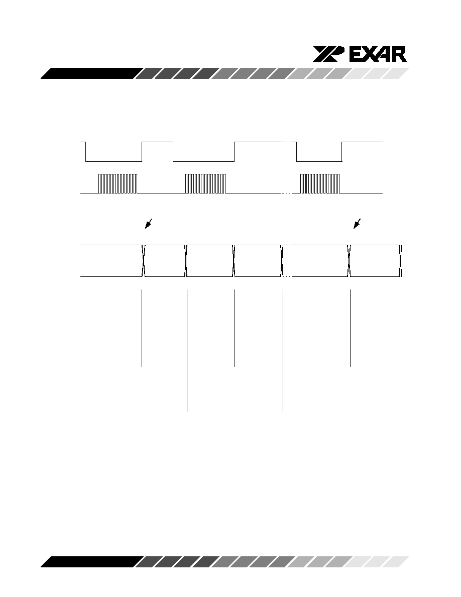
Figure 13. 3-Channel CDS Pixel Clamp Synchronization and ADC Latency Timing
CCDOUT
(Parallel RGB)
BSAMP
Pixel (n)
Pixel (n+1)
Pixel (n+2)
Pixel (n+3)
ADCCLK
VSAMP
Pixel (n+4)
ADC Samples Green
7 ADCCLK Latency
R
e
d
P
i
x
e
l
(
n
)
G
r
n
P
i
x
e
l
(
n
)
B
l
u
P
i
x
e
l
(
n
)
R
e
d
P
i
x
e
l
(
n
+
1
)
G
r
n
P
i
x
e
l
(
n
+
1
)
CCDOUT
(Green Input)
VSAMP
BSAMP
G
r
n
P
i
x
e
l
(
n
+
1
)
Pixel (n)
Pixel (n+1)
Pixel (n+2)
Pixel (n+3)
ADCCLK
Pixel (n+4)
7 ADCCLK Latency
Pixel (n+5)
Pixel (n+6)
G
r
n
P
i
x
e
l
(
n
-
3
)
G
r
n
P
i
x
e
l
(
n
-
2
)
G
r
n
P
i
x
e
l
(
n
-
1
)
Pixel (n+7)
Pixel (n+8)
G
r
n
P
i
x
e
l
(
n
)
Figure 14. 1-Channel CDS Pixel Clamp Synchronization and ADC Latency Timing
XRD9814B/9816B
32
Rev. 1.00
CISOUT
(Green Input)
Pixel (n)
Pixel (n+1)
Pixel (n+2)
Pixel (n+3)
ADCCLK
VSAMP
Pixel (n+4)
7 ADCCLK Latency
Pixel (n+5)
Pixel (n+6)
G
r
n
P
i
x
e
l
(
n
-
3
)
G
r
n
P
i
x
e
l
(
n
-
2
)
G
r
n
P
i
x
e
l
(
n
-
1
)
Pixel (n+7)
Pixel (n+8)
G
r
n
P
i
x
e
l
(
n
+
1
)
G
r
n
P
i
x
e
l
(
n
)
CISOUT
(Parallel RGB)
Pixel (n)
Pixel (n+1)
Pixel (n+2)
Pixel (n+3)
ADCCLK
VSAMP
Pixel (n+4)
ADC Samples Green
7 ADCCLK Latency
R
e
d
P
i
x
e
l
(
n
)
G
r
n
P
i
x
e
l
(
n
)
B
l
u
P
i
x
e
l
(
n
)
R
e
d
P
i
x
e
l
(
n
+
1
)
G
r
n
P
i
x
e
l
(
n
+
1
)
Figure 15. 3-Channel S/H Synchronization and ADC Latency Timing
Figure 16. 1-Channel S/H Synchronization and ADC Latency Timing

XRD9814B/9816B
33
Rev. 1.00
(Pin 40)
SCLK
(Pin 41)
SDI
A2
A1
A0
PB9
PB8
PB7
PB6
PB5
PB4
PB3
PB2
PB1
PB0
LOAD
(Pin 39)
tplw
tlch
tlcs
tdh
tds
Rising edge loads last 13
Data bits
13 Data Bits
SCLK/
DB12/DB14
(Pin 45)
SDI/
DB13/DB15
(Pin 44)
A2
A1
A0
PB9
PB8
PB7
PB6
PB5
PB4
PB3
PB2
PB1
PB0
LOAD
(Pin 39)
tplw
tlch
tdh
tds
tlcs
tlch
Rising edge loads last 13
Data bits
13 Data Bits
Figure 17. Write Timing (INSEL = 0)
Figure 18. Write Timing (INSEL = 1)
XRD9814B/9816B
34
Rev. 1.00
LOAD
SCLK
001XXXXXXXXX1
SDI
000XXXXXXXXXX
001XXXXXXXXX0
ADC Output Data
Cfig2
Not Valid
Cfig1
Not Valid
Output
(DBx)
ADC Output Data
Reg data
Reg data
XRD9814B/9816B Read Back Timing
Write to Cfig2, bit0 to
enable readback &
Address Cfig2
for register
read-back
Address Cfig1
for register
read-back
Write to Cfig2 bit0 to
enable ADC output data
& disable read-back
mode
This step can be repeated for all
registers before exiting to normal
mode
Note: If any bits of Cfig2 were
programmed prior to readback mode,
they must be re-programmed when
exiting read-back
Read-back
Cfig2 data
Read-back
Cfig1 data
Enables Read-back
Disables Read-back
Figure 19. XRD9814B/9816B Read-Back Timing

XRD9814B/9816B
35
Rev. 1.00
OEB
ADCCLK
DB13:0/
DB15:0
LOAD
LOAD = HI
TRI-STATE
TRI-STATE
tlz
tod
thz
N
N+1
DB13/15:DB0 (N-7)
DB13/15:0 (N-6)
OEB
ADCCLK
LOAD
LOAD = HI
TRI-STATE
TRI-STATE
tlz
tod
thz
N
N+1
N-7
(MSB 8-BITS)
N-7
(LSB 6/8-BITS)
N-6
(MSB 8-BITS)
N-8
(LSB 6/8-BITS)
tod
DB13:0/
DB15:0
High Bits
Low Bits
Figure 20. ADC Digital Output Timing (OUTSEL = 0)
Figure 21. ADC Digital Output Timing (OUTSEL = 1)

XRD9814B/9816B
36
Rev. 1.00
RED
GRN
BLU
ADCOUT
ADCCLK
VSAMP
7 ADCCLK Latency
tstl
1
2
3
4
5
6
7
8
9
10
11
GRN
BLU
Dummy
1
2
3
4
5
6
7
8
9
10
11
ADCCLK/SYNCHRONIZATION EVENTS
N-1
N
N+1
N+2
N+3
N
N
N
Non Valid Data
Beginning of Synchronization / Samples Green (N-1) / Converts Unkown Dummy Value
Samples Blue (N-1) / Converts Green (N-1)
Samples Red (N) / Converts Blue (N-1)
Synchronization / Samples Green (N) / Converts Red (N)
Necessary / No Sampling Events Occur
Samples Blue (N) / Converts Green (N)
Samples Red (N+1) / Converts Blue (N)
Synchronization / Samples Green (N+1) / Converts Red (N+1)
Dummy Pixel (N-1) Valid Generated From ADCCLK #2
GRN Pixel (N-1) Valid Generated From ADCCLK #3
BLU Pixel (N-1) Valid Generated From ADCCLK #4
Note: Green Channel is Synchronized on the First Rising Edge of ADCCLK After the Falling Edge of VSAMP
12
13
14
12
13
14
N-1
N-1
N-1
RED Pixel (N) Valid Generated From ADCCLK #5
GRN Pixel (N) Valid Generated From ADCCLK #6
BLU Pixel (N) Valid Generated From ADCCLK #7
CCD
tap
Figure 22. XRD9814B/XRD9816B Pipeline Latency

XRD9814B/9816B
37
Rev. 1.00
D
a
t
a
b
u
s
(
A
S
I
C
)
XRD9814B/XRD9816B
Data 14/16 - 8 Bit
Ext Serial Load
Control Signals
Avdd
A
v
d
d
Dvdd
D
v
d
d
D
g
n
d
A
g
n
d
c1
c2
c3
c4
c1=c3=0.1uF
c2=c4=0.01uF
c
r
e
f
c
a
p
p
c
a
p
n
Red(+)
Red(-)
Grn(+)
Grn(-)
Blu(+)
Blu(-)
0
.
1
u
F
2
.
2
u
F
0
.
1
u
F
2
.
2
u
F
0
.
1
u
F
2
.
2
u
F
0.1uF
2.2uF
No Connect
No Connect
No Connect
No Connect
C
C
D
/
C
I
S
XRD9814B/XRD9816B
Data 14/16- 8 Bit
Ext Serial Load
Control Signals
Avdd
A
v
d
d
Dvdd
D
v
d
d
c1
c2
c3
c4
c1=c3=0.1uF
c2=c4=0.01uF
Red(+)
Red(-)
Grn(+)
Grn(-)
Blu(+)
Blu(-)
D
a
t
a
b
u
s
(
A
S
I
C
)
0
.
1
u
F
2
.
2
u
F
0
.
1
u
F
2
.
2
u
F
0
.
1
u
F
2
.
2
u
F
0.1uF
2.2uF
No Connect
No Connect
100pF
100pF
No Connect
No Connect
C
C
D
/
C
I
S
c
r
e
f
c
a
p
p
c
a
p
n
A
g
n
d
D
g
n
d
Application Notes
Figure 23. Single Channel DC-Coupled Mode
Figure 24. Single Channel AC-Coupled Mode

XRD9814B/9816B
38
Rev. 1.00
XRD9814B/XRD9816B
Data 14/16-8 Bit
Ext Serial Load
Control Signals
Avdd
A
v
d
d
Dvdd
D
v
d
d
D
g
n
d
A
g
n
d
c1
c2
c3
c4
c1=c3=0.1uF
c2=c4=0.01uF
c
r
e
f
c
a
p
p
c
a
p
n
Red(+)
Red(-)
Grn(+)
Grn(-)
Blu(+)
Blu(-)
0
.
1
u
F
2
.
2
u
F
0
.
1
u
F
2
.
2
u
F
0
.
1
u
F
2
.
2
u
F
0.1uF
2.2uF
C
C
D
/
C
I
S
D
a
t
a
b
u
s
(
A
S
I
C
)
XRD9814B/XRD9816B
Data 14/16-8 Bit
Ext Serial Load
Control Signals
Avdd
A
v
d
d
Dvdd
D
v
d
d
D
g
n
d
A
g
n
d
c1
c2
c3
c4
c1=c3=0.1uF
c2=c4=0.01uF
c
r
e
f
c
a
p
p
c
a
p
n
Red(+)
Red(-)
Grn(+)
Grn(-)
Blu(+)
Blu(-)
D
a
t
a
b
u
s
(
A
S
I
C
)
0
.
1
u
F
2
.
2
u
F
0
.
1
u
F
2
.
2
u
F
0
.
1
u
F
2
.
2
u
F
0.1uF
2.2uF
100pF
100pF
100pF
100pF
100pF
100pF
C
C
D
/
C
I
S
Figure 25. Triple Channel DC-Coupled Mode
Figure 26. Triple Channel AC-Coupled Mode

XRD9814B/9816B
39
Rev. 1.00
INSEL/OUTSEL Data Output Format
There are two control signals for setting the output data
format and the serial load control. INSEL is used to
select the mode for programming the serial port. To
use the external pins sdi, sclk and load, INSEL must
be low (Figure 17). When INSEL is set to high, DB13/
sdi and DB12/sclk become inputs through the bi-
directional output bus to load the internal control
registers (Figure 18). The load pin is still used to latch
the data. This helps to reduce the pin count require-
ments for the ASIC that drives the XRD9814B/9816B.
OUTSEL is used to select the output data format of the
XRD9814B/9816B. The XRD9814B/9816B supports
14/16-bit parallel and 8-bit nibble output modes. When
OUTSEL is low, the output bus is standard 14/16-bit
parallel (Figure 20). To use the 8-bit nibble output
mode, OUTSEL must be set high (Figure 21). In either
14/16-bit or 8-bit nibble applications, the output bus is
tri-stated when the bi-directional serial load signal is
pulled low.
Insel
sdi
sclk
load
DB13/DB15
DB0
XRD9814B/
XRD9816B
Outsel
DB12/DB14
14/16-Bit Parallel
Digital
ASIC
External Serial Load
Insel=0, Outsel=0
Figure 27. 14/16-Bit Output (OUTSEL=0), External Serial Load (INSEL=0)
Insel
sdi
sclk
load
DB13/DB15/sdi
DB0
XRD9814B /
XRD9816B
Outsel
DB12/DB14/sclk
14/16-Bit Parallel
Bi-Directional Serial
Load
Digital
ASIC
No Connect
Insel=1, Outsel=0
No Connect
Figure 28. 14/16-Bit Output (OUTSEL=0), Bi-Directional Serial Load (INSEL=1)

XRD9814B/9816B
40
Rev. 1.00
Insel
sdi
sclk
load
DB13/DB15
DB6/DB8
XRD9814B /
XRD9816B
Outsel
DB12/DB14
8-Bit Nibble
Digital
ASIC
External Serial Load
Insel=0, Outsel=1
Figure 29. 8-Bit Nibble Output (OUTSEL=1), External Serial Load (INSEL=0)
Insel
sdi
sclk
load
DB13/DB15/sdi
DB6/DB8
XRD9814B /
XRD9816B
Outsel
DB12/DB14/sclk
8-Bit Nibble
Bi-Directional Serial
Load
Digital
ASIC
No Connect
Insel=1, Outsel=1
No Connect
Figure 30. 8-Bit Nibble Output (OUTSEL=1), Bi-Directional Serial Load (INSEL=1)

XRD9814B/9816B
41
Rev. 1.00
XRD9814B 1 Channel CIS No Clamp, AVDD = DVDD = 5V, Fs = 6MSPS, 2V Reference
DNL PLOT
-1.5
-1
-0.5
0
0.5
1
1.5
0
4
3
7
8
7
4
1
3
1
1
1
7
4
8
2
1
8
5
2
6
2
2
3
0
5
9
3
4
9
6
3
9
3
3
4
3
7
0
4
8
0
7
5
2
4
4
5
6
8
1
6
1
1
8
6
5
5
5
6
9
9
2
7
4
2
9
7
8
6
6
8
3
0
3
8
7
4
0
9
1
7
7
9
6
1
4
1
0
0
5
1
1
0
4
8
8
1
0
9
2
5
1
1
3
6
2
1
1
7
9
9
1
2
2
3
6
1
2
6
7
3
1
3
1
1
0
1
3
5
4
7
1
3
9
8
4
1
4
4
2
1
1
4
8
5
8
1
5
2
9
5
1
5
7
3
2
1
6
1
6
9
Codes
L
S
B
Graph 1. XRD9814B 1-Channel CIS S/H No Clamp DNL Plot

XRD9814B/9816B
42
Rev. 1.00
XRD9814B 1-Channel CDS Pixel Clamp, AVDD = DVDD = 5V, Fs = 6MSPS, 2V Reference, DNL Plot
-0.6
-0.4
-0.2
0
0.2
0.4
0.6
0
4
3
7
8
7
4
1
3
1
1
1
7
4
8
2
1
8
5
2
6
2
2
3
0
5
9
3
4
9
6
3
9
3
3
4
3
7
0
4
8
0
7
5
2
4
4
5
6
8
1
6
1
1
8
6
5
5
5
6
9
9
2
7
4
2
9
7
8
6
6
8
3
0
3
8
7
4
0
9
1
7
7
9
6
1
4
1
0
0
5
1
1
0
4
8
8
1
0
9
2
5
1
1
3
6
2
1
1
7
9
9
1
2
2
3
6
1
2
6
7
3
1
3
1
1
0
1
3
5
4
7
1
3
9
8
4
1
4
4
2
1
1
4
8
5
8
1
5
2
9
5
1
5
7
3
2
1
6
1
6
9
Codes
L
S
B
Graph 2. XRD9814B 1-Channel CDS Pixel Clamp DNL Plot

XRD9814B/9816B
43
Rev. 1.00
XRD9814B 3-Channel CDS Pixel Clamp, AVDD = DVDD = 5V, Fs = 6MSPS, 2V Reference, DNL Plot
-0.8
-0.6
-0.4
-0.2
0
0.2
0.4
0.6
0.8
0
4
0
5
8
1
0
1
2
1
5
1
6
2
0
2
0
2
5
2
4
3
0
2
8
3
5
3
2
4
0
3
6
4
5
4
0
5
0
4
4
5
5
4
8
6
0
5
2
6
5
5
6
7
0
6
0
7
5
6
4
8
0
6
8
8
5
7
2
9
0
7
6
9
5
8
1
0
0
8
5
0
5
8
9
1
0
9
3
1
5
9
7
2
0
1
0
1
2
5
1
0
5
3
0
1
0
9
3
5
1
1
3
4
0
1
1
7
4
5
1
2
1
5
0
1
2
5
5
5
1
2
9
6
0
1
3
3
6
5
1
3
7
7
0
1
4
1
7
5
1
4
5
8
0
1
4
9
8
5
1
5
3
9
0
1
5
7
9
5
1
6
2
0
0
Code
L
S
B
Graph 3. XRD9814B 3-Channel CDS Pixel Clamp DNL Plot

XRD9814B/9816B
44
Rev. 1.00
Graph 4. XRD9814B 1-Channel CIS S/H No Clamp Input Referred Noise vs. Gain (1 MSPS)
XRD9814B 1CH DC CIS Input Referred Noise vs. Gain of 1.63 to 5 V/V
ADCCLK = 1MSPS, ADC Input Range = 3Vpp, AVDD = 5V, DVDD = 3V
0
0.5
1
1.5
2
2.5
3
1.63
2.75
3.88
5
Gain
R
M
S
N
o
i
s
e
(
L
S
B
)

XRD9814B/9816B
45
Rev. 1.00
Graph 5. XRD9814B 1-Channel CIS S/H No Clamp Input Referred Noise vs. Gain (6 MSPS)
XRD9814B 1CH DC CIS Input Referred Noise vs. Gain of 1.63 to 5 V/V
ADCCLK = 6MSPS, ADC Input Range = 3Vpp, AVDD = 5V, DVDD = 3V
0
0.5
1
1.5
2
2.5
3
3.5
4
1.63
2.75
3.88
5
Gain
R
M
S
N
o
i
s
e
(
L
S
B

XRD9814B/9816B
46
Rev. 1.00
AVDD = 5V, DVDD = 3V, ADC Input Range = 3Vpp
0
1
2
3
4
5
6
1.63
2.75
3.88
5
Gain
R
M
S
N
o
i
s
e
(
L
S
B
)
Input Referred Noise Red Channel
Input Referred Noise Green Channel
Input Referred Noise Blue Channel
XRD9814B 3CH CDS Input Referred Noise vs. Gain of 1.63 to 5 V/V ADCCLK = 6MSPS,
Graph 6. XRD9814B 3-Channel CDS Pixel Clamp Input Referred Noise vs. Gain

XRD9814B/9816B
47
Rev. 1.00
XRD9814B/9816B Gain vs. Gain Code
0
1
2
3
4
5
6
7
8
9
10
0
63
127
191
255
319
383
447
511
575
639
703
767
831
895
959
1023
Gain Code
G
a
i
n
red
green
blue
Graph 7. XRD9814B/9816B Gain vs. Gain Code

XRD9814B/9816B
48
Rev. 1.00
XRD9814B/9816B 3CH CDS, AVDD = 5V, DVDD = 3V, Fs = 6MSPS, 3Vpp, Gain = 0.5 - 5 V/V
Output Referred System Offset Vs. Gain
Inputs AC Coupled to Ground with 100pF Capacitors
60
65
70
75
80
85
90
95
100
0.50
0.78
1.06
1.34
1.63
1.91
2.19
2.47
2.75
3.03
3.31
3.59
3.88
4.16
4.44
4.72
5.00
Gain (V/V)
O
u
t
p
u
t
R
e
f
e
r
r
e
d
S
y
s
t
e
m
O
f
f
s
e
t
(
m
V
Red Channel Offset
Green Channel Offset
Blue Channel Offset
Graph 8. XRD9814B /9816B 3-Channel CDS Pixel Clamp System Offset vs. Gain

XRD9814B/9816B
49
Rev. 1.00
XRD9816B 3-Channel CDS Pixel Clamp Mode, AVDD = DVDD = 5V, Fs = 6MSPS, 2V Reference, DNL Plot
-1
-0.5
0
0.5
1
1.5
0
1
5
8
4
3
1
6
8
4
7
5
2
6
3
3
6
7
9
2
0
9
5
0
4
1
1
0
8
8
1
2
6
7
2
1
4
2
5
6
1
5
8
4
0
1
7
4
2
4
1
9
0
0
8
2
0
5
9
2
2
2
1
7
6
2
3
7
6
0
2
5
3
4
4
2
6
9
2
8
2
8
5
1
2
3
0
0
9
6
3
1
6
8
0
3
3
2
6
4
3
4
8
4
8
3
6
4
3
2
3
8
0
1
6
3
9
6
0
0
4
1
1
8
4
4
2
7
6
8
4
4
3
5
2
4
5
9
3
6
4
7
5
2
0
4
9
1
0
4
5
0
6
8
8
5
2
2
7
2
5
3
8
5
6
5
5
4
4
0
5
7
0
2
4
5
8
6
0
8
6
0
1
9
2
6
1
7
7
6
6
3
3
6
0
Codes
L
S
B
Graph 9. XRD9816B 3-Channel CDS Pixel Clamp DNL Plot

XRD9814B/9816B
50
Rev. 1.00
XRD9816B 1CH DC CIS Input Referred Noise vs. Gain of 1.63 to 5 V/V
ADCCLK = 1MSPS, ADC Input Range = 3Vpp, AVDD = 5V, DVDD = 3V
0
2
4
6
8
10
12
1.63
2.75
3.88
5
Gain
R
M
S
N
o
i
s
e
(
L
S
B
)
Graph 10. XRD9816B 1-Channel CIS SS/H No Clamp Input Referred Noise vs. Gain (1 MSPS)

XRD9814B/9816B
51
Rev. 1.00
XRD9816B 1CH DC CIS Input Referred Noise vs. Gain of 1.63 to 5 V/V
ADCCLK = 6MSPS, ADC Input Range = 3Vpp, AVDD = 5V, DVDD = 3V
0
2
4
6
8
10
12
14
1.63
2.75
3.88
5
Gain
R
M
S
N
o
i
s
e
(
L
S
B
)
Graph 11. XRD9816B 1-Channel CIS SS/H No Clamp Input Referred Noise vs. Gain (6 MSPS)

XRD9814B/9816B
52
Rev. 1.00

XRD9814B/9816B
53
Rev. 1.00
NOTICE
EXAR Corporation reserves the right to make changes to the products contained in this publication in order to improve
design, performance or reliability. EXAR Corporation assumes no responsibility for the use of any circuits described
herein, conveys no license under any patent or other right, and makes no representation that the circuits are free of
patent infringement. Charts and schedules contained here in are only for illustration purposes and may vary depending
upon a user's specific application. While the information in this publication has been carefully checked; no
responsibility, however, is assumed for in accuracies.
EXAR Corporation does not recommend the use of any of its products in life support applications where the failure
or malfunction of the product can reasonably be expected to cause failure of the life support system or to significantly
affect its safety or effectiveness. Products are not authorized for use in such applications unless EXAR Corporation
receives, in writing, assurances to its satisfaction that: (a) the risk of injury or damage has been minimized; (b) the
user assumes all such risks; (c) potential liability of EXAR Corporation is adequately protected under the
circumstances.
Copyright 2002 EXAR Corporation
Datasheet November 2002
Reproduction, in part or whole, without the prior written consent of EXAR Corporation is prohibited.