 | ÐлекÑÑоннÑй компоненÑ: XR17D154 | СкаÑаÑÑ:  PDF PDF  ZIP ZIP |
Äîêóìåíòàöèÿ è îïèñàíèÿ www.docs.chipfind.ru
Exar
Corporation 48720 Kato Road, Fremont CA, 94538
·
(510) 668-7000
·
FAX (510) 668-7017
·
www.exar.com
xr
XR17D154
UNIVERSAL (3.3V AND 5V) PCI BUS QUAD UART
JUNE 2004
REV. 1.2.0
GENERAL DESCRIPTION
The XR17D154
1
(D154) is a quad PCI Bus Universal
Asynchronous Receiver and Transmitter (UART) with
same package and pin-out as the Exar XR17C158,
XR17D158 and XR17C154. The device is designed
to meet today's 32-bit PCI Bus and high bandwidth
requirement in communication systems. The global
interrupt source register provides a complete interrupt
status indication for all 4 channels to speed up
interrupt parsing. Each UART is independently
controlled and has its own 16C550 compatible 5G
register set, transmit and receive FIFOs of 64 bytes,
fully programmable transmit and receive FIFO trigger
levels, transmit and receive FIFO level counters,
automatic hardware flow control with programmable
hysteresis, automatic software (Xon/Xoff) flow
control, IrDA (Infrared Data Association) encoder/
decoder, 8 multi-purpose inputs/outputs and a 16-bit
general purpose timer/counter.
N
OTE
:
1 Covered by U.S. Patents #5,649,122, #5,949,787
APPLICATIONS
·
Universal Form Factor PCI Bus Add-in Card
·
Remote Access Servers
·
Ethernet Network to Serial Ports
·
Network Management
·
Factory Automation and Process Control
·
Point-of-Sale Systems
·
Multi-port RS-232/RS-422/RS-485 Cards
FEATURES
·
High Performance Quad PCI UART
·
Universal PCI Bus Buffers - Auto-sense 3.3V or 5V
Operation
·
32-bit PCI Bus 2.3 Target Signalling Compliance
·
A Global Interrupt Source Register for all 4 UARTs
·
Data Transfer in Byte, Word and Double-word
·
Data Read/Write Burst Operation
·
Each UART is independently controlled with:
16C550 Compatible 5G Register Set
64-byte Transmit and Receive FIFOs
Transmit and Receive FIFO Level Counters
Automatic RTS/CTS or DTR/DSR Flow Control
Automatic Xon/Xoff Software Flow Control
Automatic RS485 Half-duplex Control Output
with Selectable Turn-around Delay
Infrared (IrDA 1.0) Data Encoder/Decoder
Programmable Data Rate with Prescaler
Up to 6.25 Mbps Serial Data Rate at 8X
·
Eight Multi-Purpose Inputs/outputs
·
General Purpose 16-bit Timer/Counter
·
Sleep Mode with Automatic Wake-up
·
EEPROM Interface for PCI Configuration
·
Same package and pin-out as the XR17D158,
XR17C158 and XR17C154 (20x20x1.4mm 144-
TQFP)
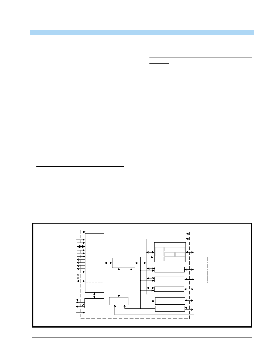
F
IGURE
1. B
LOCK
D
IAGRAM
TMR CK
Device
Configuration
Registers
XTAL1
XTAL2
Crystal Osc/Buffer
UART Channel 0
TX0, RX0, DTR0#,
DSR0#, R TS0#,
CTS0#, CD0#, RI0#
PCI Local
Bus
Interface
Configuration
Space
Registers
.
M PIO0- M PIO7
M ulti-purpose
Inputs/Outputs
TX3, RX3, DTR3#,
DSR3#, R TS3#,
CTS3#, CD3#, RI3#
UART Channel 3
UART Channel 2
UART Channel 1
16-bit
Tim er/Counter
EECK
EEDI
EEDO
EECS
EEPROM
Interface
64 Byte TX FIFO
64 Byte R X FIFO
BRG
IR
ENDE C
TX & RX
UART
Regs
VCC (Core
Logic)
GND
ENIR
CLK (33M Hz)
RST#
AD[31:0]
C/BE[3:0]#
PAR
FRAME#
IRDY#
TRDY#
DEVSEL#
STOP#
IDSEL
PERR#
SERR#
INTA#
3.3V or 5V
(PCI VI/O
Power Supply)
XR17D154
xr
UNIVERSAL (3.3V AND 5V) PCI BUS QUAD UART
REV. 1.2.0
2
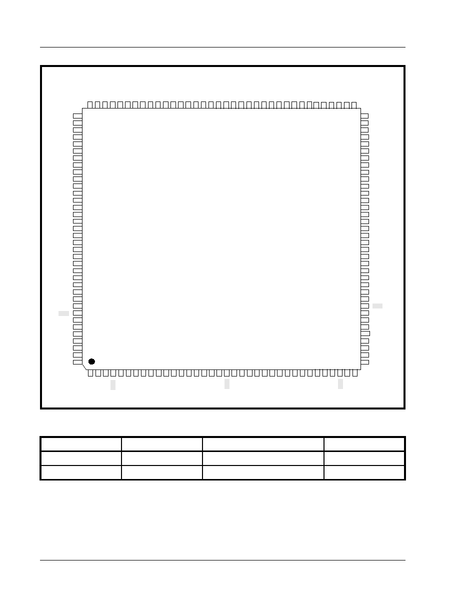
F
IGURE
2. P
IN
O
UT
OF
THE
D
EVICE
ORDERING INFORMATION
P
ART
N
UMBER
P
ACKAGE
O
PERATING
T
EMPERATURE
R
ANGE
D
EVICE
S
TATUS
XR17D154CV
144-Lead TQFP
0°C to +70°C
Active
XR17D154IV
144-Lead TQFP
-40°C to +85°C
Active
GN
D
MPIO5
GND
TMRCK
ENIR
10
8
10
7
10
6
10
5
10
4
10
3
10
2
10
1
10
0
99
98
97
96
95
94
93
92
91
90
89
88
87
86
85
84
83
82
81
80
79
MPI
O
0
MPI
O
1
VC
C
GN
D
1
2
3
4
5
6
7
8
9
10
11
12
13
14
15
16
17
18
19
20
21
22
23
24
25
26
27
28
29
30
AD
2
4
CB
E
3
I
D
SEL
VI
O
GN
D
AD
2
3
AD
2
2
AD
2
1
AD
2
0
AD
1
9
AD
1
8
AD
1
7
AD
1
6
CB
E
2
FR
A
M
E
#
I
RDY
#
TR
D
Y
#
D
E
V
SEL
#
VI
O
ST
O
P
#
PER
R
#
SER
R
#
PAR
CB
E
1
AD
1
5
AD
1
4
AD
1
3
AD
1
2
AD
1
1
GND
VCC
MPIO7
MPIO6
MPIO4
53
54
55
56
57
58
59
60
61
62
63
64
65
66
67
68
69
70
71
72
EECS
EEDI
EECK
EEDO
VCC
TEST#
XTAL1
XTAL2
128
127
126
125
124
123
122
121
120
119
118
117
116
115
114
113
112
111
110
109
31
32
33
34
AD
1
0
AD
9
AD
8
VI
O
35
36
GN
D
CB
E
0
MPI
O
2
78
77
76
75
74
73
M
P
I
O
3
AD7
AD6
AD5
AD4
AD3
AD2
AD1
AD0
VIO
37
38
39
40
41
42
43
44
45
46
47
48
49
50
51
52
AD26
AD27
AD28
AD29
AD30
AD31
VIO
GND
CLK
RST#
144
143
142
141
140
139
138
137
136
135
134
133
132
131
130
129
INTA#
AD25
NC
NC
NC
NC
NC
NC
NC
NC
RX0
CTS0#
DSR0#
CD0#
RI0#
RTS0#
DTR0#
TX0
RX
1
CT
S
1
#
TX
1
DT
R
1
#
RT
S
1
#
RI
1#
CD1
#
DS
R1
#
NC
NC
NC
NC
NC
NC
NC
NC
NC
NC
NC
NC
NC
NC
NC
NC
RX
2
CT
S
2
#
TX
2
DT
R
2
#
RT
S
2
#
RI
2#
CD2
#
DS
R2
#
RX3
CTS3#
DSR3#
CD3#
RI3#
RTS3#
DTR3#
TX3
NC
NC
NC
NC
NC
NC
NC
NC
XR17D154
144-TQFP
xr
XR17D154
REV. 1.2.0
UNIVERSAL (3.3V AND 5V) PCI BUS QUAD UART
3
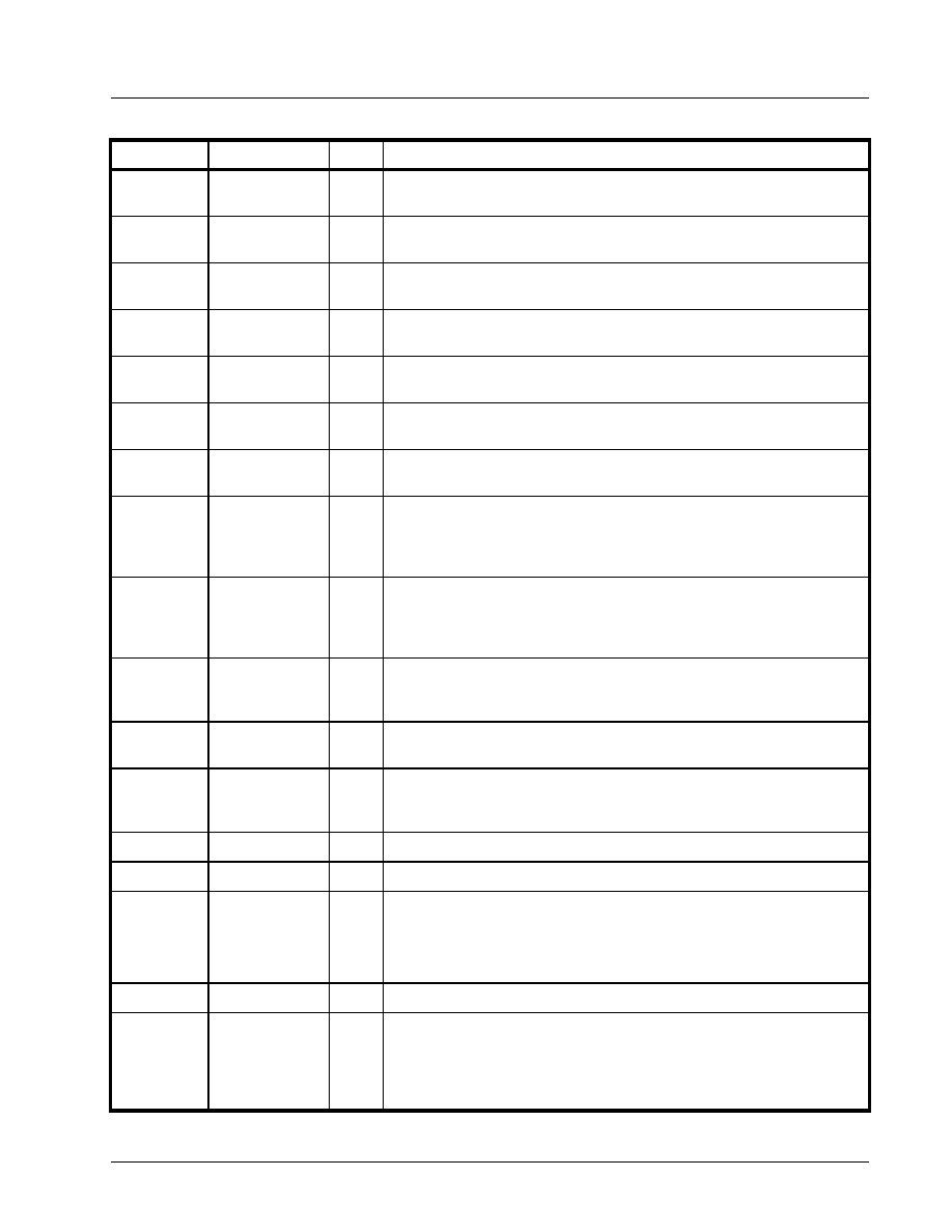
PIN DESCRIPTIONS
N
AME
P
IN
#
T
YPE
D
ESCRIPTION
PCI LOCAL BUS INTERFACE
RST#
134
I
PCI Bus reset input (active low). It resets the PCI local bus configuration
space registers, device configuration registers and UART channel registers
to the default condition.
CLK
135
I
PCI Bus clock input of up to 33.34MHz.
AD31-AD25,
AD24,
AD23-AD16,
AD15-AD8,
AD7-AD0
138-144,
1,
6-13
26-33
37-44
IO
Address data lines [31:0] (bidirectional).
FRAME#
15
I
Bus transaction cycle frame (active low). It indicates the beginning and dura-
tion of an access.
C/BE3#-
C/BE0#
2,14,25,36
I
Bus Command/Byte Enable [3:0] (active low). This line is multiplexed for bus
Command during the address phase and Byte Enable during the data phase.
IRDY#
16
I
Initiator Ready (active low). During a write, it indicates valid data is present
on data bus. During a read, it indicates the master is ready to accept data.
TRDY#
17
O
Target Ready (active low).
STOP#
21
O
Target request to stop current transaction (active low). 5
IDSEL
3
I
Initialization device select (active high).
DEVSEL#
18
O
Device select to the XR17D154 (active low).
INTA#
133
OD
Device interrupt from XR17D154 (open drain, active low).
PAR
24
IO
Parity is even across AD[31:0] and C/BE[3:0]# (bidirectional, active high).
PERR#
22
O
Parity error indicator to host (active low). Optional in bus target application.
SERR#
23
OD
System error indicator to host (open drain, active low). Optional in bus target
application.
MODEM OR SERIAL I/O INTERFACE
TX0
125
O
UART channel 0 Transmit Data or infrared transmit data. Normal TXD output
idles HIGH while infrared TXD output idles LOW.
RX0
132
I
UART channel 0 Receive Data or infrared receive data. Normal RXD input
idles HIGH. The infrared pulses typically idle LOW but can be inverted inter-
nally prior the decoder by FCTR[4].
RTS0#
127
O
UART channel 0 Request to Send or general purpose output (active low).
CTS0#
131
I
UART channel 0 Clear to Send or general purpose input (active low).
DTR0#
126
O
UART channel 0 Data Terminal Ready or general purpose output (active
low).
DSR0#
130
I
UART channel 0 Data Set Ready or general purpose input (active low).
CD0#
129
I
UART channel 0 Carrier Detect or general purpose input (active low).
RI0#
128
I
UART channel 0 Ring Indicator or general purpose input (active low).
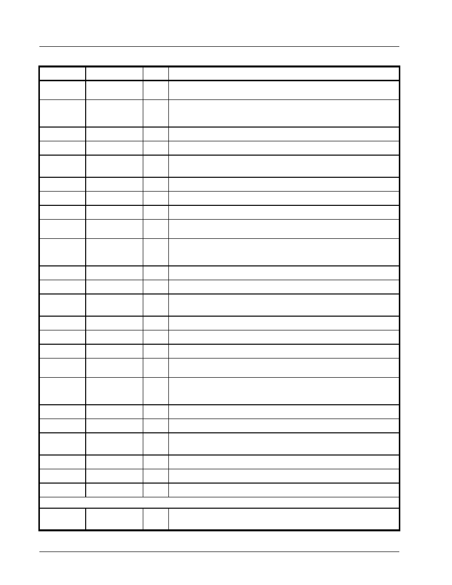
XR17D154
xr
UNIVERSAL (3.3V AND 5V) PCI BUS QUAD UART
REV. 1.2.0
4
TX1
106
O
UART channel 1 Transmit Data or infrared transmit data. Normal TXD output
idles HIGH while infrared TXD output idles LOW.
RX1
99
I
UART channel 1 Receive Data or infrared receive data. Normal RXD input
idles HIGH. The infrared pulses typically idle LOW but can be inverted inter-
nally prior the decoder by FCTR[4].
RTS1#
104
O
UART channel 1 Request to Send or general purpose output (active low).
CTS1#
100
I
UART channel 1 Clear to Send or general purpose input (active low).
DTR1#
105
O
UART channel 1 Data Terminal Ready or general purpose output (active
low).
DSR1#
101
I
UART channel 1 Data Set Ready or general purpose input (active low).
CD1#
102
I
UART channel 1 Carrier Detect or general purpose input (active low).
RI1#
103
I
UART channel 1 Ring Indicator or general purpose input (active low).
TX2
88
O
UART channel 2 Transmit Data or infrared transmit data. Normal TXD output
idles HIGH while infrared TXD output idles LOW.
RX2
81
I
UART channel 2 Receive Data or infrared receive data. Normal RXD input
idles HIGH. The infrared pulses typically idle LOW but can be inverted inter-
nally prior the decoder by FCTR[4].
RTS2#
86
O
UART channel 2 Request to Send or general purpose output (active low).
CTS2#
82
I
UART channel 2 Clear to Send or general purpose input (active low).
DTR2#
87
O
UART channel 2 Data Terminal Ready or general purpose output (active
low).
DSR2#
83
I
UART channel 2 Data Set Ready or general purpose input (active low).
CD2#
84
I
UART channel 2 Carrier Detect or general purpose input (active low).
RI2#
85
I
UART channel 2 Ring Indicator or general purpose input (active low).
TX3
62
O
UART channel 3 Transmit Data or infrared transmit data. Normal TXD output
idles HIGH while infrared TXD output idles LOW.
RX3
55
I
UART channel 3 Receive Data or infrared receive data. Normal RXD input
idles HIGH. The infrared pulses typically idle LOW but can be inverted inter-
nally prior the decoder by FCTR[4].
RTS3#
60
O
UART channel 3 Request to Send or general purpose output (active low).
CTS3#
56
I
UART channel 3 Clear to Send or general purpose input (active low).d.
DTR3#
61
O
UART channel 3 Data Terminal Ready or general purpose output (active
low).
DSR3#
57
I
UART channel 3 Data Set Ready or general purpose input (active low).
CD3#
58
I
UART channel 3 Carrier Detect or general purpose input (active low).
RI3#
59
I
UART channel 3 Ring Indicator or general purpose input (active low).
ANCILLARY SIGNALS
MPIO0
108
I/O
Multi-purpose input/output 0. The function of this pin is defined thru the Con-
figuration Register MPIOSEL, MPIOLVL, MPIOINV, MPIO3T and MPIOINT
PIN DESCRIPTIONS
N
AME
P
IN
#
T
YPE
D
ESCRIPTION
xr
XR17D154
REV. 1.2.0
UNIVERSAL (3.3V AND 5V) PCI BUS QUAD UART
5
MPIO1
107
I/O
Multi-purpose input/output 1. The function of this pin is defined thru the Con-
figuration Register MPIOSEL, MPIOLVL, MPIOINV, MPIO3T and MPIOINT.
MPIO2
74
I/O
Multi-purpose input/output 2. The function of this pin is defined thru the Con-
figuration Register MPIOSEL, MPIOLVL, MPIOINV, MPIO3T and MPIOINT.
MPIO3
73
I/O
Multi-purpose input/output 3. The function of this pin is defined thru the Con-
figuration Register MPIOSEL, MPIOLVL, MPIOINV, MPIO3T and MPIOINT.
MPIO4
68
I/O
Multi-purpose input/output 4. The function of this pin is defined thru the Con-
figuration Register MPIOSEL, MPIOLVL, MPIOINV, MPIO3T and MPIOINT.
MPIO5
67
I/O
Multi-purpose input/output 5. The function of this pin is defined thru the Con-
figuration Register MPIOSEL, MPIOLVL, MPIOINV, MPIO3T and MPIOINT.
MPIO6
66
I/O
Multi-purpose input/output 6. The function of this pin is defined thru the Con-
figuration Register MPIOSEL, MPIOLVL, MPIOINV, MPIO3T and MPIOINT.
MPIO7
65
I/O
Multi-purpose input/output 7. The function of this pin is defined thru the Con-
figuration Register MPIOSEL, MPIOLVL, MPIOINV, MPIO3T and MPIOINT.
EECK
116
O
Serial clock to EEPROM. An internal clock of CLK divide by 256 is used for
reading the vendor and sub-vendor ID and model number during power up or
reset. However, it can be manually clocked thru the Configuration Register
REGB.
EECS
115
O
Chip select to a EEPROM device like 93C46. It is manually selectable thru
the Configuration Register REGB. Requires a pull-up 4.7K
resistor for
external sensing of EEPROM during power up. See DAN112 for further
details.
EEDI
114
O
Write data to EEPROM device. It is manually accessible thru the Configura-
tion Register REGB. The D154 auto-configuration register interface logic
uses the 16-bit format.
EEDO
113
I
Read data from EEPROM device. It is manually accessible thru the Configu-
ration Register REGB.
XTAL1
110
I
Crystal of up to 24MHz or external clock input of up to 50MHz for data rates
up to 6.25Mbps at 5V and 8X sampling. See AC Characterization table. Cau-
tion: this input is not 5V tolerant at 3.3V.
XTAL2
109
O
Crystal or buffered clock output.
TMRCK
69
I
16-bit timer/counter external clock input.
ENIR
70
I
Infrared mode enable (active high). This pin is sampled during power up, fol-
lowing a hardware reset (RST#) or soft-reset (register RESET). It can be
used to start up all 4 UARTs in the infrared mode. The sampled logic state is
transferred to MCR bit-6 in the UART. Software can override this pin thereaf-
ter and enable or disable it.
TEST#
111
I
Factory Test. Connect to VCC for normal operation.
VCC
64, 90, 112
PWR
5V or 3.3V power supply for the core logic. This power supply determines
the VOH level of the non-PCI bus interface outputs. Note that VCC
VIO for
normal device operation and see Table 1 for valid combinations of VCC and
VIO.
See "Application Examples" on page 8.
However, VCC must equal VIO
if sleep mode is used. See Sleep Mode section on
page 19
.
PIN DESCRIPTIONS
N
AME
P
IN
#
T
YPE
D
ESCRIPTION
Document Outline